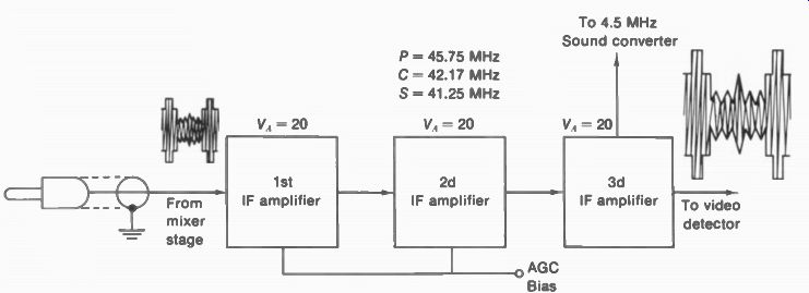
As shown in Fig. 23-1, this section amplifies the IF signal output from the mixer stage on the rf tuner. A short length of coaxial cable feeds the tuner output to the first IF amplifier. For any channel in the VHF or UHF bands, the rf picture carrier signal is converted by the tuner to 45.75 MHz for the picture IF amplifier. This section is also called the video IF amplifier, since the composite video signal is the envelope of the modulated picture IF signal.
Practically all the gain and selectivity of the receiver is provided by the IF section. With tubes, 2 or 3 IF stages are used. Typical miniature glass pentodes are the 4DK6 and 6JC6A. With transistors, 3 or 4 IF stages are needed. With integrated circuits, one IC chip contains all the IF amplifier stages. When solid-state amplifiers are used, the entire picture IF section is generally on one small board or module (Fig. 23-2) with the video detector. Details of the picture IF amplifier circuits are explained in the following topics:
23-1 Functions of the picture IF section
23-2 Tuned amplifiers
23-3 Single-tuned circuits
23-4 Double-tuned circuits
23-5 Neutralization of transistor IF amplifiers
23-6 The picture IF response curve
23-7 IF wave traps to reject interfering frequencies
23-8 Picture IF amplifier circuits
23-9 IC unit for the picture IF section
23-10 Picture IF alignment
23-11 Troubles in the picture IF amplifier
FIGURE 23-1 PICTURE IF AMPLIFIER SECTION WITH THREE TUNED STAGES.
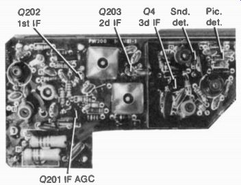
FIGURE 23-2 IF BOARD WITH TRANSISTOR AMPLIFIERS. (RCA)
23-1 Functions of the Picture IF Section
The main function is to amplify the modulated IF signal enough to drive the detector. With a 0.5-mV picture IF signal from the mixer, the IF amplifier can provide an overall voltage gain of 8,000, for 4 V into the video detector diode.
Then the video signal output of the detector is amplified for 100-V p-p video signal at the picture tube for good contrast.
The intermediate frequencies. The standard value specified by the EIA for the IF picture carrier is 45.75 MHz in all television receivers. The associated IF sound carrier is automatically 4.5 MHz below, at 41.25 MHz. These values were adopted in the year 1950, raising the intermediate frequencies from the old value of 25.75 MHz for the IF picture carrier. In general, the intermediate frequencies should be as high as possible but below the lowest rf channel. The IF band at approximately 41 to 47 MHz is just below channel 2 at 54 to 60 MHz.
The IF sound signal. For intercarrier sound, the IF sound signal at 41.25 MHz is amplified with the IF picture signal at 45.75 MHz in the common IF stages. Both the sound and picture IF signals can be amplified just by having enough bandwidth. The relative gain for the IF sound at 41.25 MHz is only 5 to 10 percent in the IF picture amplifier. Color receivers have a separate diode converter for the 4.5-MHz intercarrier sound, as shown in Fig. 23-1. In mono-chrome receivers, the 4.5-MHz sound is obtained from the video detector diode.
The IF color signal. With the IF picture carrier at 45.75 MHz, the IF color subcarrier is automatically 3.58 MHz below, at the frequency of 45.75 - 3.58 = 42.17 MHz. For color receivers, the IF color signal at 42.17 MHz is amplified as part of the IF picture signal. Remember that the 3.58-MHz color subcarrier signal is combined with the luminance signal as part of the composite video signal that modulates the picture carrier. Therefore, the IF picture signal at 45.75 MHz includes the color signal. The only requirement in the IF section is that it have enough bandwidth for the required gain at 42.17 MHz.
In summary, then, the important intermediate frequencies to remember are: 45.75 MHz for picture signal 42.17 MHz for color signal 41.25 MHz for sound signal 23-2 Tuned Amplifiers Each IF stage is a tuned amplifier. This means the gain is determined by a resonant circuit tuned to the intermediate frequencies. The tuned circuit provides an ac load impedance for the amplifier, only for the IF signal. The dc resistance of an IF coil is practically zero.
The way that a resonant LC circuit is used as the ac load impedance for the output of a tuned amplifier is illustrated in Fig. 23-3 for tubes and Fig. 23-4 for transistors. In both cases the IF coil L, tunes with the stray capacitance C, for resonance. In this example, the resonant frequency f r iS 43 MHz.
It should be noted that f r usually is not at 45.75 MHz for any of the IF tuned circuits. The reason is that the IF response is only 50 percent for the picture carrier, in order to compensate for the vestigial sideband transmission.
The tuned circuit is an application of parallel resonance, because the source of ac signal is outside the LC circuit. For parallel resonance, the impedance Z,. is maximum at the resonant frequency. Then the resonant circuit provides the load impedance needed for gain in the amplifier stage. A typical value of Z1 , is 6,000 Ohm. This value is an ac load impedance that cannot be measured with an ohmmeter.
In Fig. 23-3, L, tunes with C, to form the resonant plate load for the pentode IF amplifier.
Pentodes are used because their high plate resistance shunting the tuned circuit allows a high Q for parallel resonance. R, is a plate decoupling resistor which isolates the ac signal of the tuned circuit from the dc supply, in order to prevent feedback between stages. Cf is the bypass for Rf. Note that Cf is actually part of the tuned circuit, as it returns L, to C, for the IF signal. If Cf opens, then the resistance of Rf becomes part of the tuned circuit, resulting in low Q and practically no IF gain.
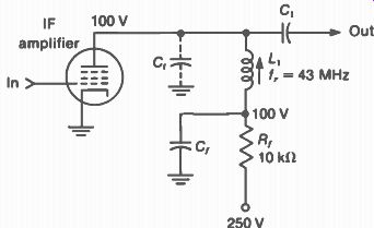
FIGURE 23-3 PARALLEL RESONANT CIRCUIT AS TUNED LOAD IMPEDANCE FOR PLATE OF
PENTODE TUBE.
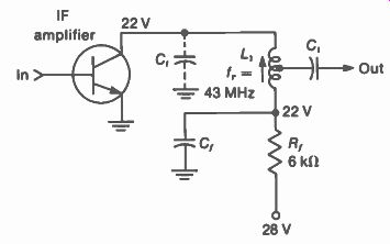
FIGURE 23-4 PARALLEL RESONANT CIRCUIT AS TUNED LOAD IMPEDANCE FOR COLLECTOR
OF TRANSISTOR. NOTE TAP ON L, FOR BASE OF NEXT STAGE.
In Fig. 23-4, the resonant circuit of L, with C, forms the collector load for IF output signal from the transistor amplifier. C, couples :he IF signal to the base of the next stage. The CE (common-emitter) circuit is used. The idea of the parallel resonant circuit as the collector load impedance is the same as the plate load impedance for a tube. Note the lower values of dc supply voltage for the transistor, compared with tubes.
The plate or collector side of L, is called the high side of the tuned circuit. This end has the IF signal voltage. The opposite end is the low side because it is grounded for ac signal by the bypass capacitor Cf . Impedance matching. In Fig. 23-4 the output connection for C, is tapped down on the IF coil L,. The purpose is to provide a stepdown of impedance from the collector to the base of the next transistor. A typical collector output resistance in the CE circuit is 50 k-o, while the base input resistance may be 1 k-o.
In Fig. 23-4, L, is connected as a step down autotransformer. All the turns serve as the primary for the collector load. However, only those turns between the tap and the low end of the coil are used as the secondary for output to the base. Another method is to use a stepdown transformer with separate primary and secondary windings. Also, a tapped voltage divider of R or C can be connected across the IF coil. In all cases, the purpose is to step down the impedance in the collector output circuit to the base input circuit of the next stage.
Dc voltages. In a tuned amplifier, the dc plate voltage or collector voltage has practically the same value as the dc supply voltage at the low side of the tuned circuit. The reason is that the IF coil has no appreciable /R drop for dc voltage because of its low resistance.
In Fig. 23-3, the plate supply voltage at the low end of R f is 250 V. This value is dropped to 100 V for the tuned circuit because of the IR drop of 150 V across R f. The 150-V drop across the 10 k-o of R f means the dc plate current / _p is 150 V/10 k-o = 15 mA. The dc plate voltage of 100 V at the high side of L, is the same as the 100 V at the low end because L, has a dc resistance of less than 1 11.
FIGURE 23-5 IF AMPLIFIER OPERATING CLASS A FOR MINIMUM AMPLITUDE DISTORTION.
In Fig. 23-4, the collector supply voltage at the low end of R1 is 28 V. This value is dropped to 22 V because of the IR drop of 6 V across R f.
The 6-V drop across the 1,000 ohm of R f means the dc collector current I_c. is 6 V/6,000 ohm = 0.001 A or 1 mA. The collector voltage of 22 V at the high side of L, is the same as the 22 V at the low end because of the low resistance of L. Class A amplification. Each IF stage operates class A for minimum distortion. Class A operation means that output current flows for 360°, or the full cycle of the signal.
A class A stage is biased to be on with output current flowing with or without signal input.
As shown in Fig. 23-5, the dc bias sets the operating point at the middle of the input-output operating characteristic. The modulated IF picture signal is the ac input. Then the variations of the input signal produce corresponding changes in the output. The envelope of the IF signal is actually the video signal, which must be amplified without amplitude distortion. It is especially important to avoid compressing the sync amplitudes. In addition, linear amplification prevents cross-modulation between the desired signal and an interfering signal.
FIGURE 23-6 RESPONSE FOR PARALLEL RESONANCE. (a) CIRCUIT TUNED TO 44 MHz.
WITH A 0 OF 20, (b) RESONANCE CURVE WITH MAXIMUM IMPEDANCE AT 44 MHz AND TOTAL BANDWIDTH OF 2.2 MHz.
23-3 Single-tuned Circuits
A single-tuned stage has one LC circuit as the load impedance in the output. See Fig. 23-3.
The output signal from the high side of the resonant circuit is coupled by C, to the next stage.
The function of C, as a coupling capacitor is to block the dc voltage at the plate or collector, but have low reactance for ac voltage at the IF signal frequencies. Values for C, are 100 to 200 pF. The resonant load impedance. The main features of tuned amplifiers can be illustrated by the resonant circuit in Fig. 23-6a. For a single tuned stage, this circuit is the load impedance for ac signal in the plate or collector circuit of the amplifier. It is an example of parallel resonance because the tube or transistor is the signal source outside the tuned circuit. The resonant frequency 1, = ½ pi __/ LC,. Ct is generally about 12 pF. Then the required L is 1.1 µH for the f r of 44 MHz. At f r, the impedance Z1 . is maximum for parallel resonance. A typical value for Z. is 6,000 it at the resonant frequency.
The tuned circuit provides a resonant rise in Z1 _p as shown by the response curve in Fig. 23-6b. Furthermore, the gain is directly proportional to the load impedance. For a pentode tube the voltage gain equals g„, x Z,.. With a g,„ of 8,000 µmho and a Z, of 6,000 ft the gain is 0.008 x 6,000 = 48.
0, damping, and bandwidth. Q is a figure of merit, indicating how sharp the resonance is. An IF coil generally has a Q of about 80, either by it self or in a tuned circuit with C. However, a parallel resistance such as R„ in Fig. 23-6a lowers the Q. The smaller the shunt RI , is, the lower the Q becomes. In addition, the bandwidth of the tuned circuit increases with lower Q. This effect of reducing the Q and increasing the bandwidth is called damping. In Fig. 23-6a, the 6-k-ohm value of RD reduces the Q of the tuned circuit to 20. This value is calculated as Q = XL/ R _p, where X1.
is 300 ohm and R„ is in parallel rather than in series with L. The total bandwidth Af in Fig. 23-6b is shown as 2.2 MHz. This bandwidth is calculated as f r/Q, which is 44 MHz/20 = 2.2 MHz. R1 , is a carbon resistor in parallel with the tuned circuit.
FIGURE 23-7 STAGGER TUNING OF THREE SINGLE-TUNED CIRCUITS FOR OVERALL BANDWIDTH
OF 4 MHz, CENTERED AT 40 MHz. THESE FREQUENCIES ARE NOT THE IF PASSBAND
BUT JUST A CONVENIENT EXAMPLE OF A STAGGER-TUNED AMPLIFIER.
Overall response. The overall gain of cascaded stages is the product of the values for each stage. When one stage has a gain of 24, the next is 10, and the final-stage gain is 20, the overall gain is 24 x 10 x 20 = 4,800. Also, the overall response curve for tuned amplifiers is the product of the individual response curves for each of the cascaded stages.
Stagger-tuned stages. When cascaded amplifiers are tuned to the same frequency (synchro nous tuning), the overall bandwidth shrinks drastically. The reason is that the overall gain equals the product of individual gain values, not their sum. Then the peak values become more peaked, while the low-gain frequencies become more attenuated. The sharp peak with narrow bandwidth is undesirable for the wide passband needed in the picture IF amplifier. However, the required overall response can be obtained with single-tuned stages by staggering their resonant frequencies. This procedure is illustrated in Fig. 23-7 for three single-tuned stages, staggered around 40 MHz, with an overall bandwidth of 4 MHz. For this triplet, one stage is tuned to the center at 40 MHz, while the other two are above and below by ± 1.72 MHz. Staggered tuning can be used for combinations of two, three, four, or five stages.
FIGURE 23-8 DOUBLE-TUNED TRANSFORMER FOR IF AMPLIFIER
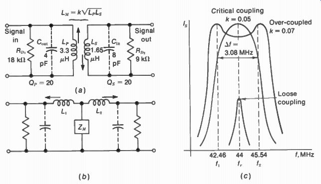
FIGURE 23-9 DOUBLE-TUNED COUPLING. (a) TRANSFORMER WITH L,. AND L, TUNED
TO THE SAME f _p (b) GENERAL FORM OF A DOUBLE-TUNED CIRCUIT WITH MUTUAL COUPLING
IMPEDANCE Zi , (c) EFFECT OF COUPLING COEFFICIENT k ON THE RESPONSE OF A DOUBLE-TUNED
CIRCUIT
23-4 Double-tuned Circuits
The advantage of these circuits is more band width, with sharper skirts on the response curve, than with single-tuned circuits. Figure 23-8 shows a typical double-tuned transformer from the output of one IF amplifier to the input of the next stage. No coupling capacitor is necessary, as the transformer couples the IF signal by induction between L _p and Lj, , while isolating the dc voltages between the two windings.
The primary and secondary inductances L 1 , and L s tune the shunt capacitances C„„, and C,„ to the desired frequency in the IF range. C_out is the output capacitance of stage 1, while C,„ is the input capacitance of stage 2. Usually, L,. and L s each have a slug for tuning the primary and secondary, so that two adjustments are needed to align the tuned transformer. The primary and secondary are both resonant at the same frequency. Note that R,C, is a decoupling filter for the dc supply voltage and R2C2 is a decoupling filter for the AGC bias line.
Double-tuned coupling. More details of resonance in the double-tuned coupling arrangement are shown in Fig. 23-9. Both primary and secondary are tuned to 44 MHz here for comparison with the single-tuned circuit of Fig. 23-6.
Coupling in the double-tuned transformer in Fig. 23-9a results from the mutual inductance Lu that links L _p and L, providing a mutual coupling impedance common to both circuits. Similar results can be obtained with other types o mutual coupling impedance, indicated by Z„ in Fig. 23-9b. Physically, Z„ can be a coupling coil or capacitor, or a combination of both L and C to function also as a wave trap to attenuate one frequency. Some double-tuned transformers have only one slug, which adjusts the coupling. Coefficient of coupling. The effect of coupling between L _p and L, in a double-tuned trans former is illustrated in Fig. 23-9c. The coupling coefficient k indicates the fraction of total flux from one coil linking the other coil. For loose coupling, the primary and secondary are far apart, with little flux linkage between L i , and L. The secondary response then has a single peak at f r like a single-tuned circuit, with low amplitude. However, as the coupling is increased by having L _p and L., closer together, the primary produces more secondary output. Also, the secondary current has a greater effect on the primary. With close coupling, then, two peaks result in the secondary output to broaden the frequency response. For a middle value called critical coupling (kr), the secondary has its maximum amplitude and greatest bandwidth without double peaks.
Impedance coupling or bandpass coupling. Examples of using a common impedance Zu for mutual coupling between two tuned circuits are shown in Fig. 23-10. This method is also called bandpass coupling because it usually has the bandwidth of an overcoupled double-tuned transformer. In Fig. 23-10a, the coil L l, is common to both tuned circuits with L,C, and L 2C2. As a result, signal voltage across L„ from one tuned circuit is coupled into the other. In Fig. 23-10b, capacitive coupling is used, with C„ common to both tuned circuits. In both circuits, R1 , is a damping resistor to provide the required bandwidth.
Link coupling. See Fig. 23-11. This method is generally used to couple the IF signal from the mixer stage on the rf tuner to the first IF stage on the main chassis. The link is a 75-ohm coaxial cable with shielded plugs at both ends. Its purpose is to couple the signal at a low impedance level. As a result, the effect of stray capacitance is minimized. With the outside shield grounded for the low-impedance line, there is no pickup of interfering signals and no radiation of the mixer output. Radiation of beat frequencies and their harmonics from the mixer can cause interference in the receiver.
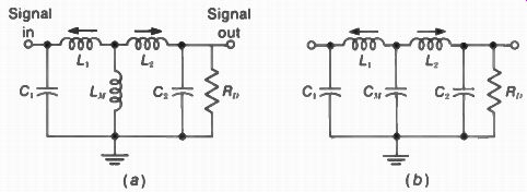
FIGURE 23-10 IMPEDANCE COUPLING WITH DOUBLE-TUNED CIRCUIT. (a) INDUCTIVE
COUPLING WITH L„; (b) CAPACITIVE COUPLING WITH Cu.
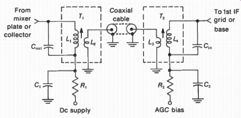
FIGURE 23-11 LINK COUPLING FROM MIXER OUTPUT ON THE RE TUNER TO THE FIRST
IF STAGE ON THE MAIN CHASSIS
Referring to Fig. 23-11, the mixer output transformer T, is on the rf tuner. The secondary winding L2 has just a few turns for a stepdown of the voltage and impedance with reference to the primary. In addition, L„, is connected to a jack on the tuner that takes the plug of the coaxial cable.
At the other end, the plug connects the IF signal to the IF transformer T., on the receiver chassis.
L. here is the primary to step up the signal voltage for the secondary L 4. This way the IF signal is coupled from the mixer output to the IF input by means of the IF cable, which can be 1 to 2 ft or more in length, without radiation or stray pickup. This link coupling generally has the response of an overcoupled stage.
Loading resistor. When either the primary or the secondary is damped with a parallel resistor of about 100 to 300 f1, the double-tuned circuit then has a single-peak response like a single tuned circuit. The reason is that the low Q in one side of the double-tuned circuit requires a much higher value of coupling between L,. and L„ for critical coupling. The actual coupling, which is part of the transformer construction, then is equivalent to loose coupling with one resonant peak. For the purpose of alignment, therefore, it is possible to peak each side of the transformer at r when a small damping resistance is temporarily shunted across the opposite side. This is also called a swamping resistor, or loading resistor.
Bifilar IF cons. This type of coil has two windings, like a transformer, but it is not double tuned. As shown in Fig. 23-12, the bifilar coil is wound with twin conductor wires, each insulated from the other. One winding is for the plate or collector, tuned to the resonant frequency as a single-tuned circuit. The other winding is for the grid or base of the next stage.
Since the IF signal is inductively coupled to the next stage, no coupling capacitor is needed.
Furthermore, the response is the same as that of a single-tuned circuit. In short, the bifilar coil provides a method of having a single-tuned amplifier without using a coupling capacitor C.
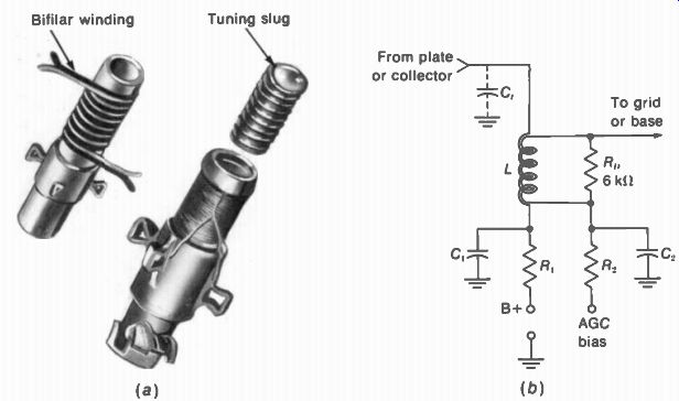
FIGURE 23-12
BIFILAR IF COIL (a) PHOTO; HEIGHT ABOUT 1l/., IN (b) SCHEMATIC SYMBOL.
FIGURE 23-13 METHODS OF NEUTRALIZING AN IF AMPLIFIER STAGE. C, FEEDS BACK NEUTRALIZING VOLTAGE OF OPPOSITE POLARITY FROM OUTPUT SIGNAL. (a) FEEDBACK VOLTAGE FROM SECONDARY OF IF TRANSFORMER; (b) TAPPED PRIMARY COIL; (c) CAPACITIVE VOLTAGE DIVIDER WITH C, AND C, ACROSS L.; (d) ANOTHER FORM OF CAPACITIVE VOLTAGE DIVIDER WITH C, AND C,.
23-5 Neutralization of Transistor IF Amplifiers
Any tuned amplifier can oscillate when enough signal is fed back from the output circuit to the input circuit in the same phase as the input signal. With vacuum tubes, triodes have appreciable feedback through the internal grid-plate capacitance C„. Pentodes seldom have feed back problems. However, PNP and NPN transistors are equivalent to triodes with relatively high capacitance between collector and base. Typical values of this internal capacitance are 5 to 20 pF. The technique of canceling the internal feedback is called neutralization. The method consists of feeding back signal voltage through an external path to cancel the internal feedback.
Four types of neutralizing circuits are shown in Fig. 23-13. Each is a method of obtaining signal voltage that is the opposite polarity from the collector signal. The neutralizing voltage is coupled back through the feedback capacitor C. A typical value for C, is 2.7 pF. It is usually a fixed value for IF amplifiers but may be variable for rf amplifiers. It should be noted that C, couples the feedback and blocks the dc collector voltage from the base. However, the feedback can be in a resistive path, without C _p as long as the dc voltages on the base are arranged to provide the correct bias for the base emitter circuit.
In Fig. 23-13a the feedback voltage is taken from the secondary L2 of the IF trans former in the collector output circuit and coupled back by the neutralizing capacitor C, to the base. The secondary voltage is phased to provide signal of opposite polarity from the collector signal in the primary. Therefore, the neutralizing signal fed back by C, cancels tie internal feedback. In Fig. 23-13b, two opposite polarities of output signal are provided by the tap on the coil L„. The top of L. is the collector side. The bottom end has signal of opposite polarity with respect to the ground at the tap.
Therefore, the neutralizing voltage fed back by C, cancels the internal feedback.
The circuits in Fig. 23-13c and d use a capacitive voltage divider for feedback. In Fig. 23-13c, the divider consists of C, and C2 across the coil L 4. Then C, at the low end of the coil feeds back the neutralizing signal voltage across C.2, while the IF voltage across C, is the output signal. Furthermore, the signal voltage at the ungrounded side of C2 is the opposite polarity from the signal across C,. Note that the isolating resistor R is needed in the collector circuit to prevent shorting the signal through the low impedance of the dc supply. Finally, the circuit in Fig. 23-13d corresponds to the capacitive voltage divider in Fig. 23-13c. The reason is that C, and C, are joined by the ground connection, forming a capacitive voltage divider across L. In this circuit, C2 has the same position as a bypass capacitor. However, its capacitance is small enough to develop neutralizing voltage that is coupled back through C, to the base.
23-6 The Picture IF Response Curve
The graph in Fig. 23-14 compares how much overall voltage amplification the IF section has for different frequencies in the passband. Note the following features of this ideal IF response curve:
1. The picture IF carrier frequency of 45.75 MHz at the side of the response curve has 50 percent of maximum IF gain. This reduced IF response for the picture carrier, and side frequencies close to it, is opposite to the effect of vestigial-sideband transmission.
2. The sound IF signal at 41.25 MHz is amplified with the picture signal for intercarrier sound. However, the relative gain is only about 10 percent for the sound signal in the picture IF amplifier section.
3. The frequency of the color subcarrier signal in the picture IF amplifier is 42.17 MHz, separated by 3.58 MHz from the picture carrier at 45.75 MHz. Note that the color frequency is at the opposite side of the IF response curve.
4. The IF bandwidth for the luminance signal is approximately 3 MHz, from 45.75 to 42.75 MHz. This IF bandwidth then corresponds to 3-MHz response for video frequencies in the picture reproduction. The bandwidth is limited to 3 MHz in the receiver, instead of 4 MHz, to minimize interference from the color signal.
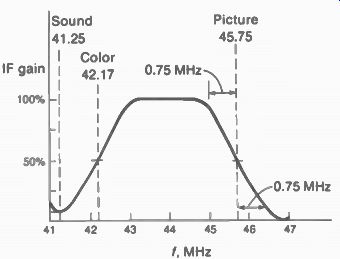
FIGURE 23-14 IDEAL PICTURE IF RESPONSE CURVE. 46 47
How 42.17 MHz corresponds to 3.58 MHz for the color signal. In the video detector, the color signal at 42.17 MHz beats with the IF picture carrier at 45.75 MHz to produce the difference frequency of 45.75 -42.17 = 3.58 MHz. The response for 42.17 MHz is generally at 50 percent.
In monochrome receivers, though, the response for 42.17 MHz is close to zero to eliminate interference from the color signal.
How 41.25 MHz corresponds to 4.5 MHz for the sound signal. Either in the video detector or in a separate diode detector as the sound converter, the sound signal at 41.25 MHz beats with the IF picture carrier at 45.75 MHz to produce the difference frequency of 45.75 - 41.25 = 4.5 MHz. For intercarrier sound, the response at 41.25 MHz is only about 10 percent or less in the common IF amplifier. The required attenuation of the sound signal is obtained by one or more wave traps tuned to 41.25 MHz.
Inversion of IF side frequencies. As an example, the rf sound carrier frequency is trans mitted 4.5 MHz higher than the rf picture carrier frequency, but in the receiver IF section the IF sound carrier at 41.25 MHz is 4.5 lower than the picture carrier at 45.75 MHz. This frequency in version results only because the local oscillator in the tuner beats above the rf signal frequencies, which is the usual case. Then higher rf frequencies are closer to the oscillator frequency, resulting in lower values for the IF difference frequencies. Additional examples are listed in Table 23-1.
The same frequency separation is maintained between the picture carrier and its side frequencies in the rf and IF signals. However, those frequencies above the picture carrier in the rf signal are below it in the IF signal. Also, the lower rf side band becomes an upper IF sideband.
How the IF side frequencies correspond to video frequencies. The highest video modulating frequencies produce side frequencies farthest from the picture carrier in the transmitted signal. Although the IF side bands are inverted, the same frequency difference compared with the carrier is maintained. Therefore, the IF side frequencies farthest from the picture carrier correspond to the highest video frequencies in the output of the video detector. In the IF response curve, these frequencies have lower numerical values, near the sound IF carrier. However, the IF gain for these frequencies determines the response for the high video frequencies that reproduce fine detail in the picture. At the opposite part of the curve, side frequencies close to the picture carrier represent the low video frequencies. The continuity between rf, IF, and video signal frequencies is illustrated by the resolution chart in Fig. 23-15.
In terms of frequency components in the detected signal, we can consider that each IF side frequency beats with the picture carrier in the video detector to produce the difference frequency. As an example, 42.75 MHz beats with 45.75 MHz in the IF signal to produce the difference frequency of 3 MHz in the video signal out of the detector. Therefore, 3-MHz band width, from 41.75 to 44.75 MHz in the IF curve, corresponds to 3-MHz response for the detected video signal, from 0 Hz or direct current up to 3 MHz for very small picture details.
TABLE 23-1 INVERSION OF IF SIGNAL FREQUENCIES
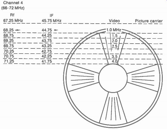
FIGURE 23-15 RESOLUTION CHART TO ILLUSTRATE THE CONTINUITY OF RF. IF. AND
VIDEO SIGNAL FREQUENCIES FOR CHANNEL 4.
Compensation for vestigial-sideband transmission. The lower video modulating frequencies up to 0.75 MHz are transmitted as double side band signals, while the higher video frequencies are transmitted as single-sideband signals, as explained in Sec. 6-2. Therefore, video frequencies above 0.75 MHz have only one-half the effective modulation of the lower-frequency double-sideband signals. If the receiver IF response were the same for all signal frequencies, the demodulated output from the video detector would be twice as great for video signals below 0.75 MHz as for the higher video frequencies.
In order to equalize the effect of vestigial sideband transmission, the overall IF response is aligned to give the picture carrier approximately 50 percent of maximum response, as shown in Fig. 23-14. As a result, the two side bands of a double-sideband signal are given an average response of 50 percent, compared with 100 percent response for the single-sideband frequencies. The relative output from the video detector, therefore, will be the same for all video modulating signals having the same amplitude, whether they are transmitted with single or double sidebands.
When the picture carrier is too high on the IF response curve, with more than 50 percent relative gain, the low video frequencies, up to 0.75 MHz, are emphasized, while higher video frequencies are attenuated. The extra gain for low video frequencies increases the contrast in the reproduced picture, but usually with excessive smear. Attenuation of the high video frequencies reduces the high-frequency detail that should make the picture sharp and clear.
When the IF gain is too low for the picture carrier frequency, the reduced response attenuates low video frequencies and the picture carrier itself.
The result is insufficient video signal and weak contrast in the picture. With zero response for the IF picture carrier there would be no picture at all.
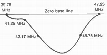
FIGURE 23-16 TYPICAL PICTURE IF RESPONSE CURVE WITH WAVE TRAP FREQUENCIES
23-7 IF Wave Traps to Reject Interfering Frequencies
A wave trap is a resonant circuit tuned to attenuate a specific frequency. Because of the wide passband in the picture IF amplifier, wave traps are needed to reduce interference and to provide the IF response for intercarrier sound. In Fig. 23-16, the trap frequencies are shown on the zero base line of the IF response. This curve is shown downward, as it would be from a negative-polarity detector. Note that the wave traps determine the shape of the overall response at both ends of the curve, for the picture carrier at one side and the color subcarrier at the other side. The trap frequencies in the picture IF amplifier are as follows:
1. 41.25 MHz is the associated sound signal for the channel to which the receiver is tuned. We want to hear the sound, but audio interference in the picture causes horizontal bars that vary with the voice or music
2. 47.25 MHz is the sound signal of the lower adjacent channel. For instance, when the receiver is tuned to channel 4, the sound signal of channel 3 may interfere with the picture. The lower adjacent sound at 47.25 MHz is always 6 MHz from the associated sound at 41.25 MHz. Since 47.25 MHz is close to the picture carrier at 45.75 MHz, tuning the adjacent sound trap affects the picture IF response for luminance signal.
3. 39.75 MHz is the picture signal of the upper adjacent channel. For instance, when the receiver is tuned to channel 3, the picture carrier of channel 4 may cause interference.
The upper adjacent picture at 39.75 MHz is always 6 MHz from the IF picture carrier at 45.75 MHz. Since 39.75 MHz is close to the color IF subcarrier at 42.17 MHz, tuning the adjacent picture trap affects the picture IF response for color signal.
Sound signal in the picture. The audio in the video produces wide horizontal bars in the picture that move in step with the modulation and disappear when there is no voice or music. The 4.5-MHz beat produces a very fine pattern of about 225 pairs of diagonal lines. The 920-kHz beat with the color signal produces approximately 60 pairs of bars. These effects of sound in the picture are illustrated in Section 19, on Troubles in the Raster and Picture. This SECTION also describes in more detail the effects of interference from adjacent channels.
The effects of sound interference in the picture can usually be produced by varying the fine-tuning control on the rf tuner. The reason is that the rf local oscillator frequency is varied to change the intermediate frequencies and their response in the IF amplifier. When the tuner has automatic fine tuning (AFT), it must be disabled to vary the oscillator frequency manually. The interference patterns are useful in determining the tuning for the best picture. The oscillator frequency is set to the point that just removes the sound interference. With the correct IF alignment, this adjustment provides good contrast with maximum bandwidth for sharp details in the picture.
Wave-trap circuits. The main types are illustrated in Fig. 23-17. In Fig. 23-17a, the parallel resonant trap is connected in series with the input to the next stage. Parallel resonance provides a very high resistance at the rejection frequency. The series connection for the trap makes it a voltage divider with the following input circuit. Most of the undesired signal voltage is developed across the high resistance of the resonant trap circuit, therefore, with little voltage coupled to the next grid circuit at the rejection frequency. The trap in Fig. 23-17b is a series resonant circuit connected in shunt with the next grid circuit. Series resonance provides a very low resistance at the rejection frequency.
At this frequency, the grid input circuit is effectively shorted by the series resonant trap. The result is very little voltage in the grid circuit at the trap frequency.
The absorption trap in Fig. 23-17c is inductively coupled to the plate load inductance.
At resonance, maximum current flows within the trap circuit. As a result, maximum current is coupled from the primary. This absorption of power from the primary causes a sharp decrease in the Q of the tuned plate load impedance, only for the trap frequency. The result is reduced gain in the IF amplifier stage for the undesired signal.
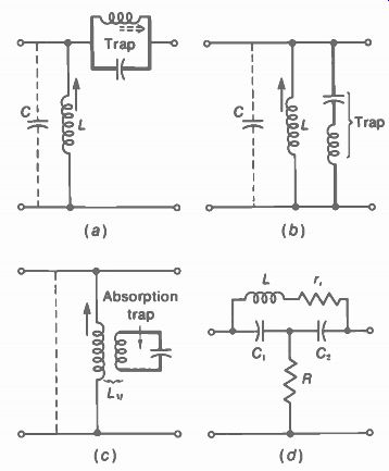
FIGURE 23-17 FOUR TYPES OF WAVE TRAPS TO REJECT AN INTERFERING FREQUENCY.
(a) PARALLEL RESONANT CIRCUIT IN SERIES WITH OUTPUT: (b) SERIES RESONANT CIRCUIT
IN SHUNT WITH OUTPUT; (c) ABSORPTION TRAP INDUCTIVELY COUPLED TO IF COIL:
(d) BRIDGED-T CIRCUIT.
The circuit in Fig. 23-17d is a bridged-T trap. The feature of this trap circuit is that it is tuned to the rejection frequency by having the value of shunt resistance R that cancels the internal resistance (r,) of the coil. Then L, C _p and form a high-0 parallel resonant circuit in series with the output.
In all cases, the trap is tuned to the frequency to be rejected. As examples, the associated sound traps are aligned at 41.25 MHz to attenuate this frequency in the picture IF response, while the lower adjacent channel sound traps are tuned to reject 47.25 MHz. The coil in the wave-trap circuit has a variable slug to tune the trap for minimum output. Each of the traps can be aligned by coupling in IF signal at the rejection frequency and tuning for minimum dc voltage output across the video detector load resistor. For this part of the IF alignment, the desired result is a dip in the output because the traps have the function of reducing the gain for the rejection frequencies.
23-8 Picture IF Amplifier Circuits
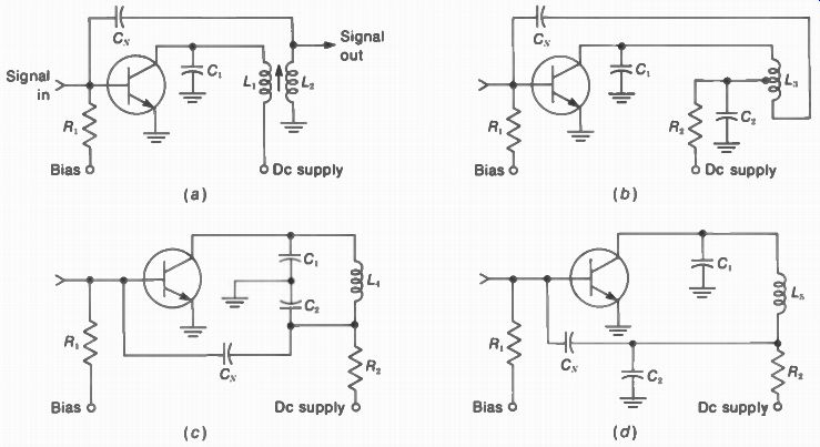
With tubes, there are usually only two stages.
Three or four IF stages are needed with transistors. With an IC unit, the entire IF amplifier section is in one chip. It should be noted that either tubes or transistors can be used for mono chrome and color receivers. Some IF circuits combine tubes and transistors.
Two-tube IF amplifier for monochrome receiver. Starting at the left in Fig. 23-18, the IF cable from the VHF tuner supplies IF signal to the first IF stage. This link couples IF signal from the mixer plate circuit on the tuner to the IF transformer i,. Note the wave traps at 39.75 MHz for the upper adjacent picture carrier and 47.25 MHz for the lower adjacent sound. The AGC bias line feeds the first IF stage and the rf amplifier in the tuner. The first IF amplifier is coupled to the second IF stage by /2„7. Only one adjustment is provided in this IF transformer to vary its coupling. The plate circuit of the second IF stage has the double-tuned transformer T 2„ to couple the IF signal into the video detector.
The overall rf and IF response curve shows a bandwidth of about 3 MHz between the 70 percent response points. The test point TP-1 at the plate of the first IF amplifier is used to obtain the response of the link circuit alone, including the mixer plate transformer, not shown here. This circuit provides the required bandwidth, with the slope of the side skirts adjusted by the wave traps. TP-2 is used to feed in signal for aligning the double-tuned transformer T.,„„ alone. The overall response shown is at the test point in the video detector output. This curve shows the typical IF response for a mono chrome receiver.
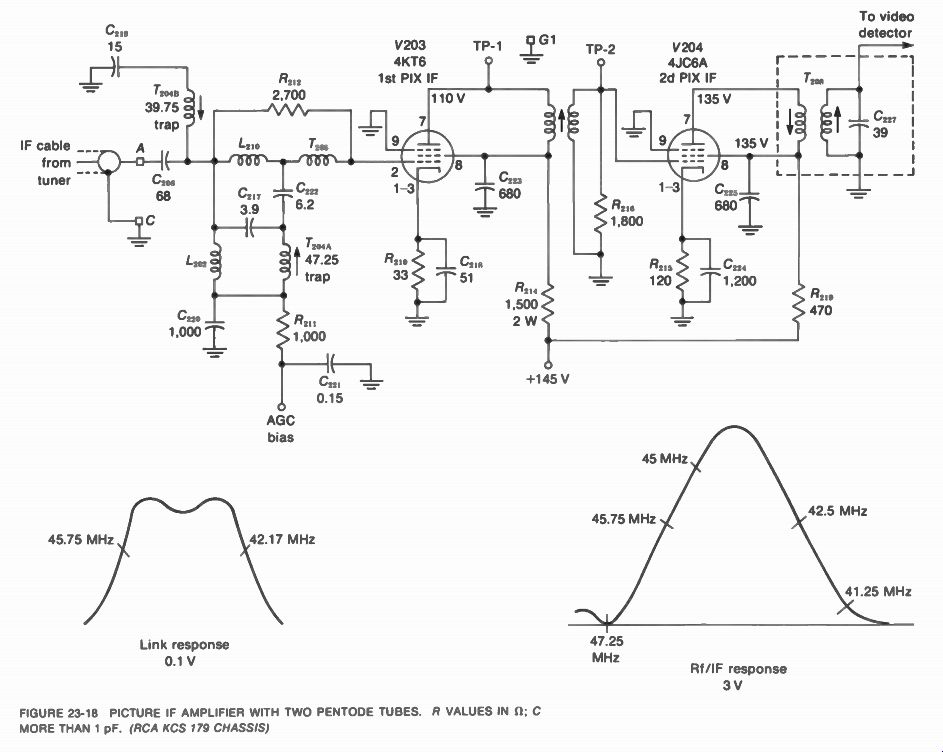
Fig. 23-18
The 4JC6A in the second IF stage is a sharp cutoff pentode. Its grid cutoff voltage is
-3 V for practically zero plate current. The 4K16 in the first IF stage has a semi-remote cutoff characteristic, with a grid cutoff of -22 V. This feature is desirable for minimum amplitude distortion as the grid voltage is varied over a wide range by the AGC bias. However, sharp cutoff tubes have higher gm, for more gain.
Transistorized IF amplifier for color receiver. See Fig. 23-19. The overall IF response for this color receiver is the same as Fig. 23-14, with 45.75 MHz for the IF picture carrier and 42.17 MHz for the IF color subcarrier at 50 per cent response at opposite sides of the curve.
The IF cable from the rf tuner supplies IF signal to the base of 0101, which is the first IF amplifier. This stage has a combination of emitter bias with R„„, and AGC bias at the base through R102. C112 is the emitter bypass capacitor for R . The IF tuning coils are L, and There are two traps in this IF input circuit: 47.25 MHz for the lower adjacent sound and 39.75 MHz for the upper adjacent picture.
The IF output of 0101 is transformer-coupled by L„ _p, to the second IF stage Q102. The feed back capacitor C, from the secondary of L _p„, to the base of 0101 is for neutralization.
Collector voltage for Q101 is from the 24-V supply shown at the top of the diagram, through R 4 and the primary of L103.
The second IF stage Q102 has the input tuned by L, and the output tuned by L,„.1 . R„, is a damping resistor for 1_ :1, and R„, damps I-104, for more bandwidth. The bias is a combination of emitter bias from R„„ and fixed bias from R„ in the voltage divider, with R117 to the 24-V supply. C, „; is the bypass capacitor for the emitter resistor R . The collector resistor R 9 Provides shunt feed for the dc collector voltage from the 24-V supply.
The IF output from the collector of Q102 goes to the base of the third IF amplifier Q104 and to a separate sound converter stage Q103, through C . This sound detector beats the 41.25-MHz IF sound signal with the 45.75-MHz picture carrier to convert to the 4.5-MHz intercarrier sound signal. A separate 4.5-MHz sound converter is generally used in color receivers, instead of using the video detector, in order to reduce beat-frequency interference between the sound and color signals. Since the sound takeoff is in the second IF amplifier here, this stage has the 41.25-MHz trap L,„„ in the output to attenuate the associated sound in the video signal.
The collector of Q104 feeds the IF signal to the video detector through the IF coils L, and L. This stage also couples IF signal to the AFC module for automatic fine tuning (AFT) on the local oscillator in the rf tuner. The AFC detects any difference between the IF picture carrier frequency and 45.75 MHz and provides a dc voltage to correct the oscillator frequency. This circuit is explained in Section 24, The RF Tuner.
23-9 IC Unit for the Picture IF Section Refer to Fig. 23-20. Although the IC unit is shown in two sections, this is one 20-pin dual in-line package (DIP) with all the following functions:
1. Three-stage IF amplifier. IF signal from the tuner is in at pin 6 for the first and second IF amplifiers. The amplified IF signal is out at pin 9 for the interstage coupling circuit and back into pin 13 of IC1B for the third IF amplifier.
2. Video detector. The video signal output at pin 19 goes to the video amplifier.
3. AGC. The IF AGC is internal, but the AGC output is also supplied at pin 4 of IC1A for the rf tuner.
4. Sound converter with a 4.5-MHz IF amplifier providing output at pin 2 on IC1B for the audio detector in a separate module for the sound signal.
5. 3.58-MHz chroma signal is out at pin 3 of IC1B for the chroma bandpass amplifier in a separate module for chrominance signal.
6. IF picture carrier signal is out at pin 14 of IC1B for the AFT or AFC module that corrects the frequency of the local oscillator in the rf tuner.
7. The regulator stage Q1 connected between terminals 15 and 18 provides steady dc supply voltage for the amplifier stages in the IC1B section.
Although the IC unit provides miniaturized transistor amplifier circuits, the pin connections must go to external circuits for the dc supply voltages and for the IF tuned circuits. In the IF input circuit for pin 6, the IF coils L1, L 2, and L3 are adjusted for the proper bandwidth between the IF picture carrier at 45.75 MHz and the IF color subcarrier at 42.17 MHz. The vari able capacitor C12 is a trimmer to place these frequencies at 50 percent response. The wave traps T, and T 2 are adjusted to attenuate the upper adjacent picture at 39.75 MHz and the lower adjacent sound at 47.25 MHz. In the inter stage coupling circuit between pin 9 on IC1A and pin 13 on IC1B, the IF transformer L„ and IF coils L, are adjusted for a symmetrical response curve. This coupling circuit also has the wave trap T, to reduce the associated sound signal at 41.25 MHz to 5 to 10 percent response for intercarrier sound.
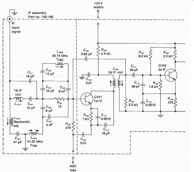
FIGURE 23-19 TRANSISTORIZED PICTURE IF AMPLIFIER CIRCUIT R VALUES IN i).
C LESS THAN 1 IN µF. (ZENITH COLOR TV CHASSIS 23 DC14)
23-10 Picture IF Alignment
Correct alignment of the picture IF stages is necessary for a good picture, since the composite video signal is the envelope of picture carrier
signal amplified in the IF section. In the modulated signal, those sideband frequencies farthest from the 45.75-MHz picture IF carrier correspond to the highest video frequencies. If these frequencies are missing or attenuated, the picture will not have horizontal detail. In color receivers, when the IF color subcarrier at 42.17 MHz is missing or attenuated, there will be no color or weak color.
At the opposite end of the IF response curve, those frequencies close to the IF carrier at 45.75 MHz correspond to the low video frequencies that reproduce large areas of picture information. When the IF response for the picture carrier is less than 50 percent, this attenuation causes a weak picture, with little contrast. Too much gain at 45.75 MHz allows strong contrast, but usually with reduced detail and smear in the picture. In addition, bars in the picture and 920-kHz beat can result from misadjustment of the sound traps.
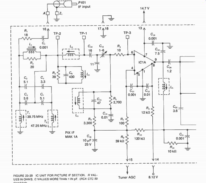
FIGURE 23-20 IC UNIT FOR PICTURE IF SECTION. R VALUES IN OHMS. C VALUES MORE
THAN 1 IN pF. (RCA CTC 59 CHASSIS)
Actually, the overall response of the IF section is more important than the bandwidth of the video amplifier in determining the bandwidth of the composite video signal and the amount of color signal. The overall IF response curve includes all the IF tuned circuits, from the mixer output in the rf tuner to the video detector.
Visual Response Curve. Figure 23-21 shows the connections for the sweep generator and oscilloscope needed to obtain a visual response curve for the overall gain in the picture IF section. The sweep generator is necessary to supply IF signal input at all frequencies in the passband of the amplifier. The oscilloscope shows the amount of video detector output voltage at the different IF signal frequencies.
This voltage indicates IF gain, since the more IF input signal to the detector, the greater its dc output voltage. With the generator supplying signal frequencies that are continuously sweeping through the IF range at the rate of 60 Hz, the detector output is a dc voltage that varies in amplitude at the rate of 60 Hz.
The visual alignment method is generally necessary to adjust double-tuned stages. Furthermore, we can see the bandwidth and relative gain at the important frequencies of 45.75 MHz for the picture carrier, 42.17 MHz for the color subcarrier, and 41.25 MHz for the associated sound. A typical sweep generator is shown in Fig. 23-22.
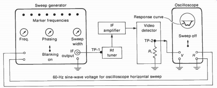
FIGURE 23-21 SWEEP GENERATOR AND OSCILLOSCOPE CONNECTIONS FOR OVERALL IF
RESPONSE CURVE. TP-1 IS TEST POINT 1 AT MIXER GRID ON RF TUNER. TP-2 IS DETECTOR
OUTPUT. DC BIAS VOLTAGE AND MARKER OSCILLATOR ARE NOT SHOWN SEPARATELY. AS
THEY ARE USUALLY SUPPLIED BY SWEEP GENERATOR.
The average oscilloscope has high-frequency response that is good enough for alignment.
With the vertical input of the oscilloscope connected across the dc load resistance of the dectector, the input to the oscilloscope vertical amplifier is not the IF signal but only dc voltage fluctuating at the 60-Hz modulation rate of the sweep generator. The amount of dc voltage depends on the amplitude of the signal input to the detector, which is proportional to IF gain.
Therefore, detector output indicates the IF amplifier response. Actually, the low-frequency response of the oscilloscope is important because the visual response curve shows a graph of detector dc output voltages, varying at 60 Hz.
Disable the horizontal scanning. This precaution prevents radiation from the horizontal deflection circuits from producing spikes on the response curve, making the curve difficult to mark. However, be careful not to allow the horizontal amplifier to have excessive current with out its drive from the horizontal oscillator. You can use a dummy load to keep the B+ voltage from going too high.
Dc bias adjustment. The AGC bias must be disabled so that the alignment can be done with fixed bias. This can be obtained from a bias box.
However, many sweep generators also supply the required dc bias. Normal bias and gain can be checked by observing that the oscilloscope screen has "grass," which is receiver noise, without any generator signal.
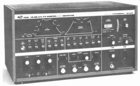
FIGURE 23-22 TYPICAL SWEEP GENERATOR FOR RF, IF, AND VIDEO RESPONSE CURVES
(B AND K DIVISION OF DYNAS CAN CORP)
IF alignment procedure. It is important to realize that just seeing a response curve is not al ways good enough. You must constantly check to make sure that the curve you see really represents the actual receiver operation with typical signal. Otherwise, you can have a pretty response curve on the oscilloscope screen but a poor picture on the screen of the picture tube.
When connecting the test equipment, make the ground connections of the probes as close as possible to the signal ground connections. You can check for proper ground connections by grasping the cables and touching the chassis to be sure your body capacitance does not affect the oscilloscope waveform. All the equipment should warm up for at least 15 min. The following steps illustrate the visual alignment procedure:
1. Connect the oscilloscope vertical input terminals to the video detector output. A test point for the video signal is usually at the top of the chassis. This test point can also be in a video amplifier dc-coupled to the video detector. Use a 10-k-o isolating resistor.
2. Connect the IF output of the sweep genera tor to the mixer grid. A test point for this connection is usually at the top of the rf tuner. The sweep cable is usually terminated in 75-O. If it is not included, a 2,200-pF blocking capacitor is used.
3. The oscilloscope internal sawtooth sweep is not used. Instead, horizontal deflection for the oscilloscope is a sine wave at 60 Hz.
There are two possibilities. If the oscilloscope has a phasing control, switch the horizontal selector switch to 60-Hz line and use this phasing control. Then no external connections to the scope horizontal input terminals are necessary. Usually, though, the oscilloscope horizontal amplifier is used for the 60-Hz voltage from the sweep generator connected to the oscilloscope, as in Fig. 23-21. Then the phasing control on the generator is used.
4. Set the frequency of the sweep generator to obtain an IF response curve on the oscilloscope screen. Use about 10-MHz sweep width to see the entire IF response. The exact frequency of the IF signal does not matter, as the frequencies must be indicated by an accurate marker generator.
5. The IF response curve is downward on the oscilloscope screen, in the negative direction, for negative dc voltage output from the video detector. For positive voltage, the curve is upward. Some oscilloscopes have a polarity-reversing switch to reverse the curve. However, make sure the curve has the correct polarity because overload distortion can turn the curve upside down.
6. Use little generator output to avoid overload distortion. Turn the oscilloscope gain up to make the curve fill the screen. Make sure that varying the generator output voltage varies the height of the response curve. A basic test for no overload is to reduce the generator signal and see if the curve becomes smaller without changing its shape.
7. Two response curves will be produced by the sweep generator, without blanking. One curve is produced by trace on one half-cycle of the 60-Hz sweep and another by retrace on the next half-cycle. First, you must make the two curves overlap by adjusting the phasing control. Then turn on the blanking to provide one curve with a zero base line. If you turn on the blanking before the curves are superimposed, the trace is a combination of parts of two curves.
8. When you mark the frequencies in the curve, they may increase from left to right or from right to left. Some generators have a reversing switch to make the frequencies increase to the right. However, either method can be used as long as the marker frequencies are correct.
It may be of interest to note that the word "sweep" is used for both the signal generator and the horizontal deflection for the oscilloscope, but the two functions are entirely different. Sweep just means to move or pass over quickly. The signal generator sweeps through a range of different frequencies. In the oscilloscope, the horizontal deflection voltage makes the electron beam move across the screen of the CRT. The internal sweep circuit generates this deflection voltage inside the oscilloscope.
Marker frequencies. The visual response curve means little until frequencies are marked.
The marker is a crystal-controlled oscillator that is mixed with the sweep signal to indicate a specific frequency accurately. A separate marker generator can be used, but many sweep generators include the markers.
The IF tuning adjustments. Adjusting the tuned coupling circuits and the wave traps changes the shape of the response curve to fit the markers correctly. It is important to realize that the wave-trap adjustments not only attenuate the undesired frequencies but determine the shape of the IF response at opposite ends of the curve, for the picture carrier and the color sub carrier.
The typical overall IF response curve for a monochrome receiver is shown in Fig. 23-18.
Here the main markers are at 50 percent response for 45.75 MHz and 5 to 10 percent response for the sound at 41.25 MHz. The response is low at 42.17 MHz, to eliminate interference from the color signal in monochrome receivers. For color receivers, the typical overall IF response curve is shown in Fig. 23-238. Here the main markers are at 50 percent response for the picture IF carrier at 45.75 MHz and 50 percent for the color subcarrier at 42.17 MHz, with 5t0 10 per cent response for the sound at 41.25 MHz. Some examples of misalignment are shown in Fig. 23-23b, c, and d.
When tuned transformers are being adjusted, the slugs may have two resonance points. They differ, though, in their effect on coupling and bandwidth. Usually, the adjustment farther away from the center of the transformer is correct.
The IF alignment is usually done in three parts:
1. Link alignment. Input signal is at the mixer grid with the oscilloscope at the first IF amplifier. A detector probe is necessary for the oscilloscope here because the IF amplifier does not rectify the signal.
2. Overall IF alignment. Input signal is at the mixer grid with the oscilloscope at the video detector output. No detector probe is needed here.
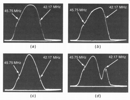
FIGURE 23-23 EFFECTS OF MISALIGNMENT ON OVERALL IF RESPONSE CURVE. (a) CORRECT
RESPONSE. NOTE THAT LOWER FREQUENCIES ARE TO THE RIGHT HERE. (b) COLOR SUBCARRER
AT 42.17 MHz TOO HIGH ON CURVE. (c)
BANDPASS TOO NARROW WITH RESPONSE TOO LOW FOR PICTURE CARRIER AND COLOR SUBCARRIER. (cf) MISTUNED SOUND TRAP AT 41.25 MHz (RCA)
3. Overall rf and IF alignment. Input signal is at the antenna input with the oscilloscope at the video detector output. This is the final test of how the IF alignment combines with the rf and mixer stages for all the tuned circuits. The input is at the rf channel frequencies, but the markers are at the IF signal frequencies.
Adjusting single-tuned stages. This can be accomplished with just a dc voltmeter and an rf signal generator, such as the marker oscillator.
A sweep generator is not needed for test signal at just one frequency. The oscilloscope is not necessary because the dc voltmeter serves as the output indicator. For an IF amplifier circuit, adjust for maximum; for a wave trap, adjust for minimum.
Causes of misalignment. When the rf tuner is replaced, it may be necessary to realign the link coupling circuit between the mixer output and the IF input. However, it is probably safe to say that misalignment is not a common cause of trouble in receivers. Once the tuned stages have been aligned, they should seldom need readjusting. When a tube or transistor is changed, the different capacitances may affect the tuning, but the IF circuits are usually designed to take this into account. Some types of trouble change the alignment, but in this case realignment is not the solution. An example is an open bypass capacitor for one of the tuned circuits. In general, when there is trouble with the picture, the cause is most likely to be a defective component, rather than misalignment.
23-11 Troubles ;n the Picture IF Amplifier
Trouble here affects the picture, while the raster is normal. No picture IF signal results in no picture, since there is no video signal for the picture tube. Also, there is no sound when a common IF stage is not operating. If there is no picture because of a defective IF stage, the raster is clean, without any snow. Insufficient gain in the IF section can also cause a weak picture.
Misalignment may result in poor picture quality, including color troubles.
The amount of picture IF signal can be checked by measuring the rectified output from the video detector. This dc voltage should be 1 to 3 V. To see the detected picture IF signal, connect an oscilloscope to the video detector output. This amplitude of composite video signal is about 3 V, peak-to-peak.
Tunable smear. This is smear in large areas of the picture that moves when the fine tuning control is varied. As the control varies the local oscillator frequency, the IF picture carrier frequency changes, resulting in a different response for the picture IF signal. Tunable smear may indicate that 45.75 MHz is too high on the IF response curve. High gain for the IF picture carrier and the sideband frequencies close to the carrier allows strong contrast in the picture, but some high-frequency detail is missing. Then the picture is not sharp and large areas may be smeared.
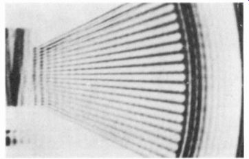
FIGURE 23-24 MULTIPLE OUTLINES CAUSED BY RINGING (RCA)
Narrow bandwidth. In this case, the IF response does not have enough bandwidth to provide normal gain for the sideband frequencies farthest from the picture carrier. These side frequencies correspond to high video frequencies. Therefore, the effect is the same as having insufficient gain for high video frequencies in the video amplifier. The result is poor horizontal resolution, with little detail. This picture cannot be sharp and clear.
Grainy picture. If the IF picture carrier is too low on the response curve, the picture will have weak contrast for large areas, with the high frequency details too strong. This effect is equivalent to having too much IF bandwidth.
The picture looks grainy, with the speckles of noise voltages too obvious. In addition, this response makes it easy to have sound interference in the picture.
Color subcarrier too low. Refer to Fig. 23-23c.
Here the color at 42.17 MHz is less than the required 50 percent response. As a result, the color in the picture can be weak.
Oscillations in the IF amplifier. Regeneration can make the IF amplifier oscillate, especially when there is an excessive peak in the IF response at one frequency. The effect in the picture is usually multiple outlines, with black streaks caused by radiation of IF signal back to the rf tuner. See Fig. 23-24.
To check whether the IF amplifier is oscillating, measure the rectified IF output across the video detector load resistor. Normally, this dc output is 1 to 3 V with a station tuned in.
When the fine tuning control is varied, the dc voltage varies as the picture carrier moves up or down the side of the IF response curve. Also, the detector output drops practically to zero when the receiver is switched to an unused channel.
However, if the detector output voltage is very high and stays about the same regardless of the rf tuning, it indicates that the IF amplifier is oscillating. The trouble can be caused by mis alignment or by a defective component that alters the alignment.
No sound with no picture. Usually, all the picture IF stages are common to the sound. As a result, no IF signal means no picture and no sound. In some cases, there may be weak sound, as sound signal can be capacitively coupled through an open stage.
SUMMARY
1. The picture IF section amplifies the IF signal output from the mixer to supply enough IF voltage for the video detector. With 0.5 my into the IF section, an IF gain of 8,000 provides 4-V output.
2. A coaxial cable connects the IF signal from the mixer on the rf tuner to the first IF amplifier. Link coupling is used for the cable, as shown in Fig. 23-11.
3. With tubes, two pentodes are generally used. With semiconductors, three or four transistors or one IC unit are needed. Usually the whole IF section is a separate module.
4. The standard frequencies are 45.75 MHz for the IF picture carrier, 41.25 MHz for the first IF sound carrier, and 42.17 MHz for the first IF color subcarrier.
5. The IF picture carrier has 50 percent response to compensate for vestigial sideband transmission. On the opposite end of the IF response curve, the IF color subcarrier also has 50 percent response. The associated sound signal is also amplified for intercarrier sound, with a response of 5 to 10 percent.
6. The IF bandwidth is about 2.5 MHz in monochrome receivers and 3.5 MHz in color receivers, to accommodate the side bands of the modulated picture carrier signal. Side frequencies close to the carrier correspond to the low video frequencies that determine contrast in the picture. Side frequencies farther from the picture carrier correspond to the high video frequencies that deter mine horizontal detail. The color subcarrier at 42.17 MHz can be considered a side frequency separated from the picture carrier by 3.58 MHz.
7. Wave traps are used in the picture IF amplifier to attenuate the associated sound at 41.25 MHz, the lower adjacent sound at 47.25 MHz, and the upper adjacent picture at 39.75 MHz. These trap frequencies are marked on the IF response curve in Fig. 23-16.
8. Each IF stage is a tuned amplifier. It has gain only for frequencies that provide a resonant rise in impedance. The IF amplifier operates class A for minimum distortion of the video envelope in the AM signal.
9. The dc voltage drop across an IF coil is practically zero. This means the dc voltage at the plate or collector is essentially the same as the supply voltage at the low end of the coil.
10. With transistor amplifiers, the IF coil is often tapped down to match the relatively high collector output resistance to the lower base input resistance of the next stage.
11. Transistor IF amplifiers are often neutralized to prevent the amplifier from oscillating. A neutralizing capacitor C„ feeds back signal from output to input, in opposite polarity from the amplified output. See Fig. 23-13.
12. In a double-tuned transformer, both L i . and L., are tuned to the same frequency.
The advantages are more bandwidth with sharper skirt selectivity than is provided by a single-tuned stage.
13. With staggered single-tuned stages, each is resonant at a different frequency to broaden the overall response.
14. The overall picture IF response can be observed with an oscilloscope connected to the video detector output, while a sweep generator at the mixer grid provides the required frequencies in the IF passband. See Fig. 23-21. Fixed bias must be used instead of AGC bias. Also, the rf local oscillator and horizontal scanning should be disabled to prevent interference in the response curve. Typical curves are shown in Fig. 23-23.
15. No output in a common IF amplifier means no picture and no sound, although the raster is normal. The raster is clean, without any snow. You can check for IF output by measuring the dc voltage across the video detector load resistor; it should be 1 to 3 V, with the rf tuner on a channel.
Self-Examination (Answers at back of guide)
Answer True or False.
1. The IF output of the mixer includes picture carrier signal at 45.75 MHz, sound carrier signal at 41.25 MHz, and color signal at 42.17 MHz.
2. Link coupling is generally used for the IF coaxial cable from the rf tuner to the first IF amplifier on the main chassis.
3 The amount of IF signal into the video detector is approximately 100 V.
4. If the IF picture carrier at 45.75 MHz is too high on the IF response curve, the picture will not have enough contrast.
5. If there is no IF gain at 42.17 MHz, the picture cannot have any color.
6. The trap frequency for the lower adjacent channel sound carrier is 47.25 MHz.
7. The intercarrier sound frequency is 4.5 MHz out of the video detector or out of a separate sound converter stage.
8. The color subcarrier frequency out of the video detector is 3.58 MHz.
9. A tuned circuit has maximum ac impedance at parallel resonance.
10. A single-tuned circuit with f,. of 44 MHz and Q of 20 has a bandwidth of 2.2 MHz.
11. A picture IF stage operates class A for minimum distortion of the envelope of the AM picture signal.
12. A smaller value of shunt damping resistance across a tuned circuit increases the bandwidth.
13. The plate voltage on a pentode IF stage is about one-half the dc voltage at the low side of the IF coil.
14. When an IF coil in the collector circuit is tapped down, this is done for impedance matching to the base of the next transistor.
15. In a double-tuned transformer, both the primary and secondary are tuned to the same frequency.
16. A wave trap is always tuned for minimum output at the trap frequency.
17. Fixed bias must be used instead of AGC bias when an IF stage is aligned.
18. Although the sound is an FM signal, it can produce audio interference in the video signal.
19. When the oscilloscope is connected to the video detector output for the IF response curve, a scope demodulator probe must be used.
20. With a visual response curve, the marker frequencies indicate where the picture carrier is.
21. The overall IF response curve from the video detector in Fig. 23-16 shows negative dc voltage out of the detector.
22. When three IF amplifiers have a voltage gain of 20 for each stage, the overall gain equals 8,000.
23. In a stagger-tuned amplifier, each stage is resonant at a slightly different frequency.
24. When an IF stage common to both the picture and sound signals is cut off, the result is no picture and no sound.
25. When an IF stage after the sound takeoff point is cut off, the result is no picture but normal sound.
26. The base-emitter bias on an NPN silicon transistor is about 0.6 V positive.
27. For forward AGC at the base of an NPN transistor, the bias becomes more positive with more signal.
28. The collector voltage is positive for an NPN transistor.
29. In the common-emitter (CE) circuit, the output resistance in the collector circuit is much higher than the input resistance in the base circuit.
30. In Fig. 23-19, the only IF stage that has AGC bias is Q101.
Essay Questions
1. Draw a typical overall IF response curve for a color receiver. Mark the following frequencies: picture carrier, associated sound carrier, and color subcarrier.
2. Give one difference between the IF response for color and monochrome receivers.
3. Repeat Table 23-1, but with the frequencies listed for channel 2 at 54 to 60 MHz.
4. Draw the schematic diagram of a single-tuned IF amplifier, using a pentode tube with a plate decoupling filter.
5. Draw the schematic diagram of a single-tuned IF amplifier, using an NPN transistor with a decoupling filter in the collector circuit.
6. Show a neutralized transistor amplifier.
7. Why is neutralization used with transistor amplifiers but not with pentodes?
8. Why is an IF coil tapped down for the next stage in transistor amplifiers? Why is this not necessary with vacuum tube amplifiers?
9. Draw the schematic diagram of a double-tuned IF stage using an NPN transistor.
10. The receiver is tuned to UHF channel 83 at 884 to 890 MHz. List the following carrier frequencies in the IF amplifier: picture carrier, color subcarrier, associated sound, lower adjacent sound.
11. What is the advantage of stagger tuning compared with synchronous tuning?
12. Give one advantage of a bifilar coil for a single-tuned circuit.
13. What is the advantage of a double-tuned amplifier compared with a single-tuned stage?
14. List three trap frequencies in the picture IF section.
15. What causes audio sound bars in the picture? Give two differences between sound bars and hum bars.
16. Name the two signals into the video detector which produce the 4.5-MHz intercarrier sound and give their frequencies. Do the same for a separate sound converter stage.
17. Why is link coupling used between the mixer output and IF input?
18. Describe briefly how to obtain the overall visual IF response curve. (a) What is the purpose of using fixed bias? (b) What is the function of the marker frequencies? (c) Why is the sweep generator at the mixer grid, instead of at the first IF stage?
19. List five controls or output terminals on a sweep generator with their functions.
20. Why is a demodulator probe needed for sweep alignment of a double-tuned coupling circuit between the mixer output and first IF stage?
21. In the IF amplifier in Fig. 23-18, which pentode stages are common to picture and sound?
22. In the transistor IF amplifier in Fig. 23-19, which IF stage is for picture alone?
23. In Fig. 23-18, give two functions for C223 at pin 8 of the first IF amplifier tube.
24. In Fig. 23-18, give the functions for T 204A , T 20411, and T2o7.
25. Name the IF stages that have AGC bias in Figs. 23-18 and 23-19.
26. In Fig. 23-20, give the functions for T _p T 2, T 4, and L„.
27. In Fig. 23-20, at which pin of the IC chip can you connect an oscilloscope to see the composite video signal?
28. Give five possible effects in the picture which result from incorrect IF response.
Problems (Answers to selected problems at back of guide)
1. For the IF response curve in Fig. 23-14, assume the overall voltage gain at 44 MHz is 8,000. How much is the gain at (a) 45.75 MHz; (b) 42.17 MHz; (c) 41.25 MHz?
2. The overall gain for the curve in Prob. 1 is reduced one-half by AGC bias. How much is the gain at 45.75 MHz, 44 MHz, 42.17 MHz, and 41.25 MHz?
3. In Fig. 23-19, when the collector current I_c. equals 5 mA for Q102, how much is its collector voltage V ?
4. Give the local oscillator frequency with rf and IF carrier frequencies for picture and sound of channels 3 and 4 when the receiver is tuned to: (a) channel 4; (b) channel 3.
5. Calculate the inductance L for resonance at 43 MHz with capacitance C of 10 pF.
6. Give the function for each of the frequencies listed below.
FREQUENCY (MHz) FUNCTION
39.75
41.25
42.17
43.75
45.75
47.25
211.25
257.00