The receiver circuits use three signals, including color. One is the FM sound
carrier, modulated with audio signal for the loudspeaker. The second is the
AM picture carrier, modulated with video signal for the picture tube. In color
receivers, the third signal is the 3.58-MHz color-plexed subcarrier. This is
part of the picture carrier signal. The three signals enable us to see the
picture and hear the sound. We consider circuits only for monochrome receivers
here, as the principles of color television and color receivers are explained
in more detail in the next two SECTIONs. It is important to realize, though,
that all the circuits for a black-and-white picture are also needed for color.
The color television picture is just a monochrome picture with color added
in the main areas of picture information.
In addition to the signal circuits, the television receiver has vertical and horizontal deflection circuits for scanning the raster. Finally, with the picture on the raster, synchronization is necessary. The deflection sync includes vertical and horizontal pulses that time the scanning circuits to hold the picture steady on the raster. The functions of the receiver circuits and controls are described in the following topics:
7-1 Types of television receivers
7-2 Receiver circuits
7-3 Signal frequencies
7-4 Intercarrier sound
7-5 Dividing the receiver into sections
7-6 Receiver controls
7-7 Receiver tubes
7-8 Solid-state devices
7-9 Special components
7-10 Printed-wiring boards
7-11 Localizing receiver troubles to one section
7-12 Multiple troubles
7-13 Safety features
7-1 Types of Television Receivers
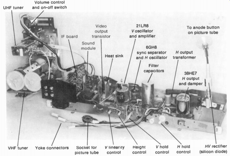
For either monochrome or color, the receiver may use tubes for all stages, have all solid-state transistors and integrated circuits, or combine tubes and transistors as a hybrid receiver. A typical hybrid chassis for a monochrome receiver is shown in Fig. 7-1.
All-tube receivers. This type applies mainly to monochrome receivers and older color receivers. All the functions are provided by about 12 tubes for monochrome and 18 tubes for color receivers. Included are multipurpose tubes with two or three stages in one envelope. The B+ for plate and screen voltage is 140 V or 280 V. Solid-state receivers. In this type, all the stages except the picture tube use semiconductor diodes, transistors, and integrated circuits. The dc supply voltage, then, is about 12 to 90 V. for collector voltage. The only heater is for the picture tube. A separate filament trans former is used, or the filament can be heated with direct current from the low-voltage power supply.
FIGURE 7-1 CHASSIS OF HYBRID RECEIVER WITH TUBES AND TRANSISTORS (MAG NAVOX
CORPORATION)
Hybrid receivers. In this type, the deflection circuits generally use power tubes, while the signal circuits use transistors and integrated circuits. These receivers usually have an ac-dc power supply, with series heaters for the tubes.
The collector voltage of 12 to 28 V for the transistors can be taken from the dc bias voltage of the horizontal deflection amplifier.
7-2 Receiver Circuits
See the block diagram in Fig. 7-2, with typical waveshapes. These circuits are essentially the same for monochrome and color receivers. For a color broadcast, the chrominance signal is part of the video signal. In monochrome receivers, however, this 3.58-MHz C signal is just not used, as the video amplifier attenuates frequencies above 3.2 MHz. The type number 18VAUP4 for the monochrome picture tube indicates that 18 in. is the screen diagonal and P4 is the phosphor for a white screen.
Antenna input. Starting with the antenna signal, the picture and sound rf carrier signals are intercepted by a common receiving antenna.
The transmission line connects the antenna to the receiver input terminals for the rf tuner.
Twin lead is generally used. This type is a balanced line, without a ground, and unshielded.
The characteristic impedance for rf is 300 ohm.
When there is a problem of interference, it may be better to use shielded coaxial cable.
This line has high attenuation of the signal, however, especially for the UHF channel frequencies. Coaxial cable has a characteristic impedance of 75 ohm. Two ungrounded screw terminals on the receiver are connections for 300-ohm twin lead. A grounded jack is for coaxial cable. To convert one type of line to the other type of connection, a balancing transformer (balun) is used. Most receivers now have an antenna jack for coaxial cable, which is generally used for master antenna and cable-television installations.
There are two tuners, one for VHF channels 2 to 13 and the other for UHF channels 14 to 83, each with its own antenna input terminals.
When the antenna and transmission line are the same for VHF and UHF, then a signal splitter at the receiver input is used to separate the signal for the two tuners.
VHF tuner. The antenna input provides rf picture and sound signals for the rf amplifier stage.
The amplified rf output is then coupled into the mixer stage. Also coupled into the mixer is the output of the local oscillator to heterodyne with the rf picture and sound signals. When the oscillator frequency is set for the channel to be tuned in, the picture and sound signals of the selected station are heterodyned down to the lower intermediate frequencies of the receiver.
The oscillator beating with the two rf carrier signals produces two IF carrier signals.
One is the picture IF signal from the rf picture signal, and the other is the sound IF signal from the sound rf signal. The original modulating in formation of the rf carrier signals is present in the IF signals out of the mixer, for both the AM picture signal and the FM sound signal. Further more, the 4.5-MHz separation between the rf carrier frequencies is maintained in the IF carrier frequencies. The intermediate frequencies in the output of the mixer stage are 45 75 MHz for the IF picture carrier and 41.25 MHz for the IF sound carrier. Note the 4.5-MHz difference between 45.75 and 41.25 MHz.
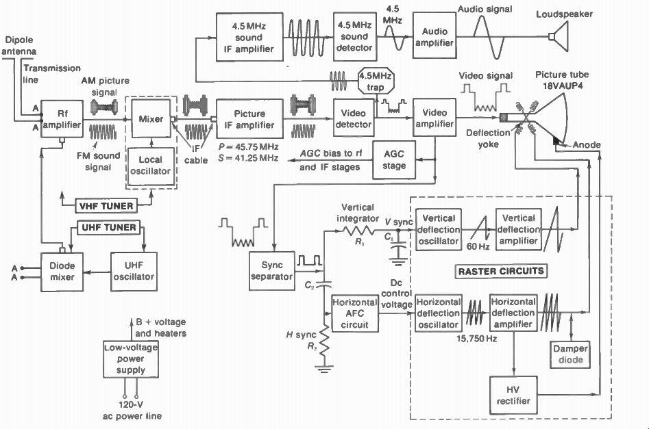
Fig. 7.2
The rf amplifier, mixer, and local oscillator stages are on an individual subchassis, called the front end, or rf tuner. Either tubes or transistors can be used. With tubes, the local oscillator and mixer functions are usually combined in one stage, called the frequency converter.
The tuner selects the channel to be received by converting its picture and sound rf carrier frequencies to the intermediate frequencies of the receiver. Then the selected signals can be amplified in the IF stages. The station selector is a ganged switch that changes the tuned circuits for the rf amplifier, mixer, and oscillator. The fine tuning control sets the oscillator frequency exactly for the best picture. It is important to note that the oscillator frequency determines which channel can be amplified by the IF section. Any problem of receiving the wrong channel is an oscillator trouble.
UHF tuner. When the VHF channel selector is set to its UHF position, the UHF tuner operates.
The antenna input is obtained from a separate UHF antenna or the splitter from a combination VHF-UHF antenna. The UHF tuner is a separate unit, including transistor oscillator and crystal diode mixer. These two stages serve as the frequency converter to heterodyne the UHF channels down to the intermediate frequencies of the receiver. The UHF oscillator is tuned for the desired UHF station.
On the UHF position of the VHF tuner, the VHF oscillator is disabled. Then the rf amplifier and mixer on the VHF tuner are tuned to the IF values of 45.75 MHz for the picture signal and 41.25 MHz for the sound signal. A short length of coaxial cable plugs into both tuners, connecting the IF output of the UHF tuner to the rf amplifier of the VHF tuner, now serving as an IF amplifier.
Picture IF signal. The picture IF amplifier includes two to four tuned stages using tubes, transistors, or an integrated circuit. The band width is enough for the IF picture signal with its side frequencies and for the IF sound signal.
The main function here is amplifying the picture IF signal from the mixer to provide several volts for the video detector. This section is also called the video IF amplifier in schematic diagrams.
The gain of the IF amplifier is controlled automatically by the AGC bias, according to the strength of the signal. A typical IF module board containing the complete picture IF amplifier section and video detector is shown in Fig. 7-3. The IF amplifier is usually connected to the mixer output on the rf tuner by a short length of coaxial cable, with a plug on both ends.
The IF value standardized by the Electronic Industries Association for the picture carrier frequency is 45.75 MHz in all receivers.
Then the sound IF carrier is automatically 41.25 MHz, separated by 4.5 MHz from the picture carrier. The chrominance signal in the IF amplifier has the frequency of 42.17 MHz, which is 3.58 MHz from the picture carrier at 45.75. The sound and color IF values are below the picture carrier frequency because the rf oscillator beats above the rf signal frequencies in the frequency conversion by the rf tuner.
Video detector. The modulated IF picture signal is rectified and filtered here to recover its AM envelope, which is the composite video signal needed for the picture tube. The main purpose of the video detector is to provide for the video amplifier the composite video with its camera signal, sync, and blanking.
For color broadcasts, the video detector output also includes the 3.58-4Hz chrominance signal. This signal is used in the color amplifier in color receivers.
Intercarrier sound. In addition to the video signal, the output of the video detector in Fig. 7-2 includes the 4.5-MHz intercarrier sound signal. All television receivers, monochrome or color, use the intercarrier method of demodulating the sound as a 4.5-MHz signal for all channels, VHF or UHF. However, color receivers have a separate 4.5-MHz sound converter, instead of using the video detector for this function. The reason is to minimize interference between the sound and color signals. The advantage of the intercarrier system is that the 4.5-MHz sound signal is automatically tuned in with the picture.
Video amplifier. Consisting of one or more stages, this section amplifies the composite video signal enough to drive the grid-cathode circuit of the picture tube. The camera signal variations change the instantaneous grid cathode voltage, modulating the intensity of beam current. Then the variations of light intensity, as the spot scans the screen, enable the picture to be reproduced on the raster.
The amount of composite video signal required for the picture tube is about 100 V peak to peak for strong contrast. Cathode drive is generally used. This requires video signal with positive sync polarity and negative white amplitudes at the picture tube cathode, as shown in Fig. 7-2. Remember that negative cathode voltage corresponds to positive voltage at the control grid, to increase the beam current for white signal amplitudes.
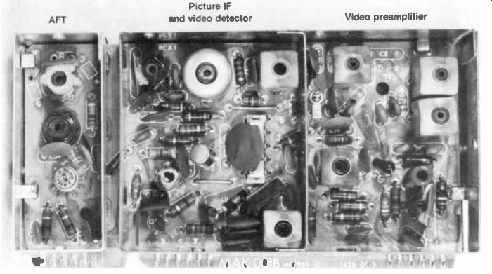
FIGURE 7-3 MODULE BOARD WITH PICTURE IF AMPLIFIER, VIDEO DETECTOR AND VIDEO
PREAMPLIFIER CIRCUITS IN COLOR RECEIVER. AFT IS AUTOMATIC FINE TUNING. THE
LENGTH OF ENTIRE BOARD IS 7 IN, (RCA)
The contrast control in the video amplifier varies the amount of video signal for the picture tube. More video signal means more contrast.
The blanking pulses in the composite video signal drive the picture tube grid-cathode voltage to cutoff, blanking out retraces. Although the sync is included in the video signal for the picture tube, the only effect of sync voltage here is to drive the grid more negative than cutoff. Note that the composite video signal is also coupled to the sync circuits (where the synchronizing pulses are separated for use in timing the receiver scanning) and to the AGC stage that produces AGC bias for the rf and IF amplifiers.
Automatic gain control. This automatic-gain control (AGC) circuit is similar to the automatic volume-control (AVC) system in AM radios. The stronger the picture carrier is, the greater the AGC bias voltage produced and the less the gain of the receiver. The result is relatively constant video signal amplitude for different carrier-signal strengths. Therefore, AGC for the picture signal is useful as an automatic control of contrast in the reproduced picture. However, the AGC circuit affects both the picture and sound, since it controls the gain of the rf and IF stages.
Synchronizing circuits. The video detector output includes the synchronizing pulses as part of the composite video signal. This signal, therefore, is also used in the sync circuits. The sync provides the timing pulses needed for controlling the frequency of the vertical and horizontal deflection oscillators.
A sync separator is a clipper stage that can separate the synchronizing pulse amplitude from the camera signal in the composite video.
Remember that the top 25 percent of the video signal amplitude is used for sync. When the tips of the video signal are clipped off and amplified, the output consists only of sync pulses.
Since there are synchronizing pulses for both horizontal and vertical scanning, Fig. 7-2 shows the output of the sync separator divided into two parts. The integrator is a low-pass RC filter circuit that filters out all but the vertical pulses from the total separated sync voltage.
Then the vertical synchronizing signals can lock in the vertical deflection oscillator at 60 Hz. For horizontal synchronization, an automatic frequency-control (AFC) circuit is used to lock in the horizontal deflection oscillator at 15,750 Hz.
Deflection circuits. As shown in Fig. 7-2 these include the vertical oscillator and amplifier for vertical scanning at 60 Hz, with the horizontal oscillator and amplifier for scanning at 15,750 Hz. For either vertical or horizontal scanning, the oscillator stage generates deflection voltage to drive the amplifier at the required frequency.
The deflection amplifiers are power output stages to provide enough scanning current in the deflection yoke for a full-sized raster.
The horizontal output circuit also includes the damper diode and high-voltage rectifier. The damper has the function of re6ucing sine-wave oscillations in the horizontal saw tooth scanning current, which occur immediately after flyback. The high-voltage rectifier produces dc anode voltage for the picture tube.
The deflection circuits produce the required scanning current and the resultant raster with or without the synchronizing signals.
Since the deflection oscillators are free-running, they do not require any external signal for operation. However, the sync is needed to hold the deflection oscillators at exactly the right frequency so that the picture information is reproduced in the correct position on the raster.
Without sync, the deflection circuits scan the raster, but the picture will not hold still.
Low-voltage supply. Two power supplies are shown in Fig. 7-2. One is the usual B+ supply for dc operating voltages on the tubes or transistors. This is the low-voltage supply because its output voltage is low compared with the high voltage supply for anode voltage on the picture tube. For sufficient brightness, the anode voltage for black-and-white picture tubes is 9 to 20 kV, while color tubes use about 18 to 25 kV.
The dc output of 140 to 280 V supplies plate voltage for vacuum tube amplifiers. Silicon diodes are generally used as the rectifiers.
For transistors and integrated circuits, the required dc supply is about 12 to 90 V, in either positive or negative polarity.
When tubes are used, the heaters can be in parallel with a 6-V winding on the power transformer, or in series for ac-dc sets. With series heaters, all the heater voltages add to equal the power-line voltage of 120 V. An open in any one heater opens the entire series string.
The heater current for a series string usually is either 450 or 600 mA. In tube sets having "instant-on" operation, the heaters have about one-half their normal voltage with the power switch off. Full power is applied when the receiver is turned on, and the tubes are on almost immediately. This feature has been developed to be similar to solid-state devices, which are on immediately because they have no heater.
High-voltage supply. The high-voltage rectifier obtains its ac input from the horizontal amplifier. This arrangement is called a flyback supply because the high voltage is generated as an induced voltage during the fast horizontal retrace.
The resultant voltage is stepped up by the horizontal output transformer for the required amount of high voltage. The rectified output is the dc anode voltage needed by the picture tube to produce brightness on the phosphor screen. Because the anode voltage depends on the horizontal output with a flyback circuit, there cannot be any brightness on the picture tube screen if the horizontal scanning circuits are not operating.
Signal voltages. For a picture without snow, the required antenna signal is about 1,000 µV or 1 mV. The signal voltage from the tuner into the IF amplifier is about 10 mV. For linear operation of the video detector diode, about 1 to 3 V of IF signal is needed. These are all rms values for the modulated picture carrier signal.
In the output of the video detector, a typical value of composite video signal for tubes is about 3 V, peak to peak, with an average dc level of about 2 V. For transistors in the video amplifier, one-half these voltages are typical values.
The peak-to-peak signal out of the video amplifier to drive the picture tube is 80 to 120 V for good contrast. The required dc level or bias for the correct brightness is about 40 V, negative at the control grid or positive at the cathode of the picture tube.
7-3 Signal Frequencies
The operation of the receiver can be examined in more detail by considering the frequencies in different sections of the receiver for picture, sound, and color.
RI and IF values. As an example, let the VHF tuner in Fig. 7-2 be set for tuning in channel 3 at 60 to 66 MHz. Then the rf amplifier and mixer input are tuned to this band of frequencies for the picture carrier (P) at 61.25 MHz and the sound carrier (S) at 65.75 MHz. The local oscillator is at 107 MHz, which is 45.75 MHz above P and 41.25 MHz above S. Similarly, for UHF channel 14 at 470 to 476 MHz, P is 471.25 MHz and S is 475.75 MHz. The UHF oscillator is at 517 MHz. Then UHF channel 14 is converted to the IF picture carrier signal at 45.75 MHz and the IF sound signal at 41.25 MHz.
In all cases the difference between P and S is exactly 4.5 MHz, for VHF or UHF channels, for color or monochrome, for rf and IF signals.
This frequency of 4.5 MHz is the intercarrier sound signal for the sound section. Inversion of the intermediate frequencies. It should be noted that the oscillator beats above the rf signal frequencies. As a result, the IF signal frequencies become inverted. In the rf signals, S is higher than P, but in the IF signals Sat 41.25 MHz is lower than P at 45.75 MHz. The reason is just that, in the rf signal, the frequency for S is closer to the oscillator frequency than P is. Then the difference is less for S. Video frequencies. When the picture carrier signal is rectified in the video detector, the carrier frequency is filtered out. The envelope is the composite video signal with camera signal, sync, and blanking. The frequencies in the cam era signal variation include high video frequencies up to 4 MHz, approximately, for horizontal details. At the low end, frequencies down to 30 Hz show shades of light and dark in the vertical direction. In addition, the dc level of the signal indicates the average brightness level.
Double superheterodyne. The feature of a superheterodyne circuit is converting the rf signal frequencies for different stations to the intermediate frequencies of the receiver. This way the rf carrier signals are all shifted in frequency to make them fit the receiver's IF amplifier, instead of changing all the tuned circuits in the receiver for each rf signal. Practically all the selectivity and all the gain of the receiver result from the IF amplification.
In a double superheterodyne circuit, the signal frequency is beat down twice for a second IF value lower than the first. The television receiver is actually a double superheterodyne for the 4.5-MHz sound signal and for the 3.58-MHz chrominance signal. These IF values are listed in Table 7-1 to illustrate the sequence of frequencies.

TABLE 7-1 THE IF SIGNAL FREQUENCIES
Picture IF value
First chrominance IF value First sound IF value Second sound IF value Second chrominance IF value
= 45.75 MHz
=42.17 MHz
= 41.25 MHz
= 4.5 MHz
= 3.58 MHz
7-4 Intercarrier Sound
Note the sequence of stages for sound in Fig. 7-2. After being amplified in the rf tuner with the picture signal, the sound signal passes through the picture IF amplifier so that both the sound and picture IF signals are coupled into the video detector. This IF amplification for both signals is accomplished by having a little more bandwidth in the picture IF amplifier to provide some gain for the sound IF signal. However, there is much more gain for the picture signal. The gain for the picture IF signal at 45.75 MHz is about 10 times more than for the sound IF signal at 41.25 MHz.
As a result, the video detector can produce the 4.5-MHz sound signal as the difference frequencies between the strong IF picture carrier beating with the weaker IF sound signal. This action corresponds to the operation of the frequency converter in the rf tuner, where the relatively strong output of the local oscillator beats with the weak rf signal.
The 4.5-MHz sound section. The 4.5-MHz wavetrap in the output of the video detector in Fig.
7-2 is the sound takeoff circuit. This resonant tuned circuit filters out the 4.5-MHz sound signal from the video frequencies. Note that the takeoff circuit, the sound IF amplifier, and the FM sound detector are always tuned t04.5 MHz. This combi nation is the mark of intercarrier sound receivers.
The sound IF stage amplifies the 4.5-MHz signal enough to drive the FM detector. This detector is necessary because the 4.5-MHz inter carrier sound is not an audio signal. The frequency modulation in the 4.5-MHz signal is the same as in the rf and first IF sound signals.
After this FM signal is detected at 4.5 MHz, the detector output is the desired audio signal.
Then the audio signal is amplified in a conventional audio amplifier to drive the loudspeaker.
Buzz in the sound. The only problem with intercarrier sound is that the vertical blanking pulses in the picture signal can interfere with the 4.5-MHz sound signal. The result is buzz at 60 Hz. It sounds like 60-Hz hum but is rougher because the buzz is produced by square waves.
The buzz is eliminated by keeping the amplitude low for the first IF sound signal and using AM rejection circuits for the 4.5-MHz FM sound signal. Many receivers have a buzz control on the back of the chassis, which is adjusted for minimum buzz.
The intercarrier buzz may increase when the picture goes to white, as the picture carrier amplitude then decreases. If the transmitter modulates white too close to zero amplitude, there will not be enough picture carrier, causing the intercarrier sound signal to be interrupted.
Split-sound receivers. Practically all television receivers use intercarrier sound, compared with the old method of split-sound. These old receivers amplified and detected the sound at its first IF value, with a separate IF amplifier tuned to 21.25 MHz. The old standard IF values were 21.25 MHz for the sound signal and 25.75 MHz for the picture signal. Split-sound receivers became obsolete when television broadcasting started to use the UHF channels from 470 to 890 MHz. At these frequencies, it is too difficult for the local oscillator in the rf tuner to tune in the sound as a separate signal.
7 - 5 Dividing the Receiver into Sections
The picture is reproduced on the screen as the combined result of the raster, video signal, and sync. These functions are summarized in Tables 7-2 and 7-3. In addition, Fig. 7-4 illustrates the successive steps in forming the raster and superimposing the picture on the raster.
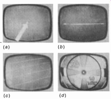
FIGURE 7-4 HOW THE RECEIVER PUTS THE PICTURE ON THE RASTER. (a) ILLUMINATION
ON SCREEN. (b) Illumination PLUS HORIZONTAL SCANNING. (c) HORIZONTAL AND VERTICAL
SCANNING TO PRODUCE THE WHITE RASTER. (d) VIDEO SIGNAL PRODUCING A PICTURE
ON THE RASTER.
Illumination. Just the spot of light on the screen in Fig. 7-4a shows that the picture tube and high-voltage supply are operating. However, it should be noted that this illustration was produced with an external high-voltage source.
The flyback supply in the receiver cannot produce high voltage without horizontal output.
-----------------
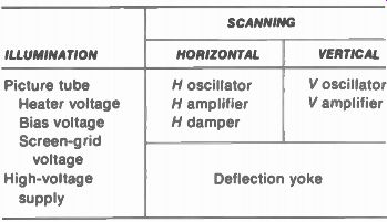
TABLE 7-2. CIRCUITS FOR THE RASTER (for block diagram in Fig. 7-2)
ILLUMINATION SCANNING HORIZONTAL VERTICAL
Picture tube Heater voltage Bias voltage Screen-grid voltage
High-voltage supply H oscillator H amplifier H damper V oscillator V amplifier Deflection yoke
-------------------
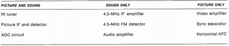
TABLE 7-3 CIRCUITS FOR THE SIGNAL (for block diagram in Fig. 7-2)
PICTURE AND SOUND Rf tuner
Picture IF and detector AGC circuit
SOUND ONLY 4.5-MHz IF amplifier 4.5-MHz FM detector Audio amplifier
PICTURE ONLY
Video amplifier
Sync separator
Horizontal AFC
------------------------
Horizontal scanning. The single horizontal line in Fig. 7-4b shows illumination and horizontal scanning. The horizontal deflection circuits, including the horizontal oscillator, amplifier, and damper stages, produce the horizontal scanning.
Vertical scanning. The vertical oscillator and amplifier stages produce vertical scanning.
Then the horizontal scanning lines fill the entire screen area from top to bottom to form the scanning raster. The white raster in Fig. 7-4c shows that the vertical and horizontal deflection circuits, the picture tube, and the high-voltage supply are operating.
Picture. Figure 7-4d shows a picture reproduced on the raster. The circuits for picture signal, from the antenna input to the picture tube grid, provide video signal for the picture information. Then the video signal voltage varies the intensity of the electron beam, while the deflection circuits produce scanning, to reproduce the picture as shades of white, gray, and black on the raster.
Deflection sync. Vertical synchronization al lows successive frames to be superimposed exactly over each other so that the picture will not appear to be rolling up or down the screen.
Horizontal synchronization prevents the line structure of the picture from tearing apart into diagonal segments. The synchronizing circuits in the receiver provide the horizontal and vertical sync for the deflection oscillators to hold the picture steady.
Circuits for the raster. In Table 7-2 only the raster circuits are listed with the requirements for illumination. Assuming that the picture tube is operating with high voltage to produce light, the horizontal and vertical deflection circuits then can produce the raster.
Circuits for signal. Table 7-3 lists these circuits as separate groups, based on the receiver block diagram in Fig. 7-2. With intercarrier sound, only the 4.5-MHz circuits and audio amplifier in the second column are for sound alone.
Almost all the signal circuits are for both picture and sound. As listed in the first column, the rf tuner, picture IF amplifier, and video detector are common to the picture and sound signals. The AGC circuit controls the gain of these rf and IF amplifiers.
Only the video amplifier is listed in the third column for picture alone, with the sync circuits to hold the picture steady. Even the video amplifier can be common to the sound, however, in receivers where the 4.5-MHz signal is taken from the video amplifier output circuit.
7-6 Receiver Controls
These can be considered in two groups: the setup adjustments mainly for the raster and the operating controls in the signal circuits. The setup adjustments for the scanning raster are usually on the rear apron of the chassis. The operating controls are in the front panel or at the side of cabinet.
Raster adjustments. The vertical height and linearity controls are adjusted to fill the screen top to bottom, with the scanning lines equally spaced for good linearity. If there is a width control, it is adjusted to make the raster just cover the left and right edges of the screen. It should be noted that the raster is the same for all stations and is present with or without signal. however, the raster with signal can be a little smaller as blanking crops the edges slightly.
If the raster is off-center, there are usually magnet rings on the neck of the picture tube that can be rotated to shift the raster vertically and horizontally. It should be noted that the horizontal hold control can shift the picture slightly with respect to the raster.
Channel selector. The VHF channel switch tunes in the desired station for channels 2 to 13.
On the UHF position of this switch, dc voltage is supplied to the UHF oscillator to operate the UHF tuner. Then the UHF channel control can be used to select any UHF channel from 14 to 83.
Fine tuning. This control provides more exact setting of the frequency for the VHF oscillator.
With intercarrier sound, the fine tuning can be set for the best picture, independently of the sound. The best picture with good contrast and fine detail results by setting the fine tuning just off the point where you see wide horizontal sound bars that move with the voice modulation.
Volume. This is a typical audio level control, usually a potentiometer to vary the signal voltage input to the first audio amplifier. Some receivers may also have a tone control to adjust the response for high audio frequencies.
Buzz. Adjust this control, if necessary, for minimum 60-Hz buzz in the sound.
Contrast. Since the receiver generally has AGC to vary the gain of the rf and IF amplifiers, the contrast control is in the video amplifier circuit to adjust the amplitude of video signal voltage for the picture tube.
Video peaking. Some receivers have this control to vary the high-frequency response of the video amplifier for sharper outlines in the picture. This control is also called fidelity, or sharpness. However, the picture may look better with reduced bandwidth and less sharpness if there is noise or interference in the signal.
AGC level. For proper range of the contrast control, the AGC level setup adjustment at the back of the chassis must be set properly. Adjust the AGC level for full contrast on the strongest station with the contrast control at maximum.
Keep the AGC level below the point of overload distortion, however, where black and white are reversed and the picture is out of sync with buzz in the sound.
Brightness. This control varies the dc bias for the grid-cathode circuit of the picture tube. Ad just for the desired overall illumination on the screen. If the picture goes completely out of focus at high brightness levels, the trouble may be insufficient high voltage or an old picture tube that probably has weak emission.
Vertical hold. This control adjusts the frequency of the vertical deflection oscillator close enough to 60 Hz to allow the sync to lock in the vertical scanning. When the picture rolls up or down, the vertical hold control is varied to make the picture stay still.
Horizontal hold. This control adjusts the horizontal deflection oscillator. When the picture shifts horizontally and tears apart into diagonal segments, the horizontal hold control is varied to establish horizontal synchronization and provide a complete picture.
It is interesting to note that many of the controls are similar in their function of varying an ac voltage level. Turning up the volume control increases the amount of audio signal for more volume. Similarly, the contrast control increases the amount of video signal for more contrast. Also, the color control increases the amount of 3.58-MHz chroma signal for more color in the picture. In addition, the height control increases the amount of vertical sawtooth scanning current for more height in the raster. A width control increases the amount of horizontal sawtooth scanning current.
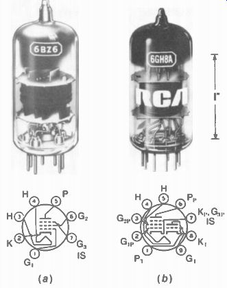
FIGURE 7-5 MINIATURE GLASS AMPLIFIER TUBES. (a)
SEVEN-PIN BASE. (b) NINE-PIN BASE. IS IS INTERNAL SHIELD.
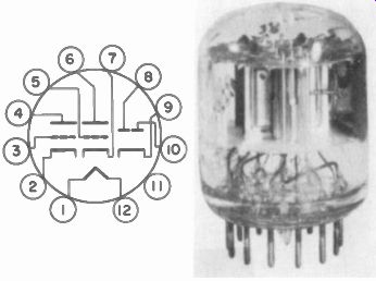
FIGURE 7-6 COMPACTRON MULTIFUNCTION TUBE 6B10.
COMBINING TWO DIODES AND TWO TRIODES. HEIGHT IS 1'/, IN. (GE)
7-7 Receiver Tubes
Where tubes are used instead of transistors to amplify the sound and picture signals, these stages are usually the miniature glass types shown in Fig. 7-5. The heater pins are 3 and 4 fo• the seven-pin base in a or 4 and 5 for the 9-pin novar base in b. The wider spacing between end pins is the guide for inserting the tube in its socket. The nine-pin tubes come in several different sizes, with a slightly larger base and larger pins for power tubes.
The 6-V tubes such as 6GH8A are for parallel heater circuits in receivers with an ac power supply using a power transformer, which includes a 6-V winding. Heater ratings such as 3BZ6, 8F07, and 17D4 are for series heater circults in those receivers that do not have a power transformer. The 3BZ6 or 66Z6 is a pentode often used in the picture IF amplifier.
The compactron tube in Fig. 7-6 combines three stages in one envelope. Note the duodecar twelve-pin base used for this type and for power tubes in general. The heaters are the end pins 1 and 12. At the opposite extreme, the nuvistor is a miniaturized tube not much larger than a transistor, often used as the triode rf amplifier in VHF tuners.
Power tubes are needed for the deflection circuits, especially in the horizontal output stage, which takes the most power from the low voltage supply. The 6JE6 in Fig. 7-7 has a maximum power rating of 30 W plate dissipation.
Average cathode current is about 350 mA. Note the plate connection to the top cap.
The damper (Fig. 7-8) in the horizontal output stage is a diode power rectifier. The 6CT3 damper tube in a has a maximum rating of A for peak plate current. Peak ratings for the semiconductor diode damper in b are 10 A for forward current and 320 V for reverse voltage.
A tube for the damper must have a high inverse-voltage rating between cathode and heater, to prevent arcing to chassis ground. A typical maximum rating is -5,500 V. The damper takes a long time to heat up because of the heavy cathode insulation.
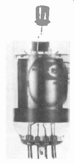
FIGURE 7-7 HORIZONTAL POWER OUTPUT TUBE 6JE6 WITH NOVAR BASE. TOP CAP IS
PLATE CONNECTION. HEIGHT IS 4 IN. (RAYTHEON COMPANY)
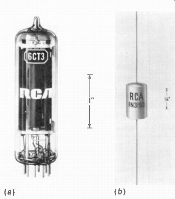
FIGURE 7-8 DAMPER DIODE FOR HORIZONTAL OUTPUT CIRCUIT. (a) TUBE (b) SILICON
DIODE (RCA)
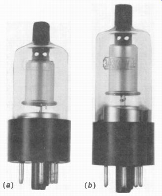
FIGURE 7-9 HIGH-VOLTAGE DIODE RECTIFIER TUBES. (a) 1G3/183 FOR MONOCHROME
RECEIVERS. (b) 3A3 FOR COLOR RECEIVERS. HEIGHT IS 4 IN. (RAYTHEONcom PANY)
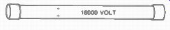
FIGURE 7-10 SILICON-DIODE STICK FOR HIGH-VOLTAGE RECTIFIER. LENGTH IS 3 IN.
CATHODE END MARKED 4 FOR DC OUTPUT.
The damper stage conducts immediately after horizontal flyback to damp the output circuit. Without damping, there are vertical, thin, white lines at the left edge of the raster, produced by oscillations in the horizontal scanning current. In addition, the rectified deflection voltage from the damper supplies boosted B+ voltage for the plate of the horizontal amplifier tube.
Finally, the damper current, while the diode is conducting, provides horizontal scanning for the left side of the raster. For this reason, the horizontal damper is also called an efficiency diode. It should be noted that when boosted B+ voltage is used for the horizontal amplifier, this stage cannot operate without the damper.
The high-voltage rectifiers in Fig. 7-9 feature very high peak inverse-voltage rating, in a flyback supply. This rating is 36 kV for the 1G3 in a. The heater power of 1.25 Vat 0.2 A is taken from the horizontal output circuit, as is the high voltage ac input of 18 kV. This tube is for a black-and-white picture tube where beam current is less than 1 mA for the rectifier's load current. For three-gun color picture tubes, the 3A3 in b has a current rating of 2 mA, with dc high-voltage output of 25 kV. Both of these tubes have an octal socket and a top cap for the plate connection. The silicon unit in Fig. 7-10 is rated at 18 kV, but ratings up to 35 kV are available.
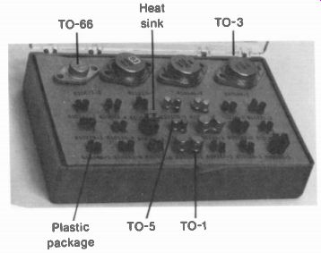
FIGURE 7-11 TRANSISTOR KIT FOR SERVICING TELEVI SION RECEIVERS 'TO IS TRANSISTOR
OUTLINE NUMBER DIAMETER OF METAL TO-3 CASE IS 1 2 IN (MAGNAVOX CORPORATION)
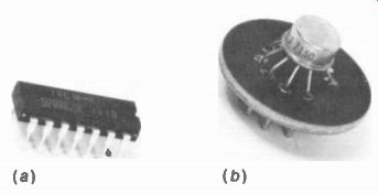
FIGURE 7-12 TYPICAL IC UNITS FOR TELEVISION RECEIVERS. (a) DUAL IN-LINE PACKAGE
(DIP). LENGTH IS 'V, IN. NOTCH AT END INDICATES PIN 1. POWER RATING IS 850
mW. (b) TO-5 PACKAGE MOUNTED ON NINE-PIN TUBE SOCKET. (SPRAGUE ELECTRIC COMPANY)
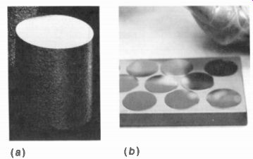
FIGURE 7-13 FORMS OF PURE SILICON (a) SOLID BAR. (b) WAFER DISKS DIAMETER
IS 1V2 IN (DOW CORNING)
7-8 Solid-State Devices
These include transistor amplifiers, diode rectifiers, and the integrated circuit (IC). Typical transistors and IC units are shown in Figs. 7-11 and 7-12.
The semiconductor elements germanium (Ge) and silicon (Si) are generally used. Silicon is a dark, crystalline solid that is brittle, like glass. A bar of pure silicon and wafer disks cut from the bar are shown in Fig. 7-13. After the sil icon is processed to alter its electrical characteristics, each disk can be cut into more than 100 sections for transistors and IC chips. An IC chip, typically 0.05 in.', combines transistors, diodes, and resistors and capacitors to form complete circuits. A transistor chip is even smaller.
The transistor was invented in 1948, using germanium. Now almost all solid-state devices use Si because it can operate at higher temperatures and has less leakage current, compared with Ge. The name "transistor" is derived from "transfer resistor." The advantages of a transistor are its small size and efficient operation.
Semiconductor devices use the electric charges in the solid material. There is no heater or cathode. Without a heater, there is no warmup time, allowing instant operation when the electrode voltages are applied. Normal life of a semiconductor device, without any troubles of opens or shorts, is probably about 20 years. The disadvantage of semiconductors is that their characteristics are sensitive to changes in temperature and that they are easily damaged by excessive heat.
More details of semiconductors can be found in transistor books and in the authors' "Basic Electronics," 3d ed. McGraw-Hill Book Company. See Bibliography at back of guide.
Doping. In their pure form, semiconductors have few free electrons in their atoms. However, impurity elements can be added to increase the number of free charges by a factor of 10 to 50 times. This doping process alters the distribution of the valence electrons in the semiconductor atoms. When electrons are added, the semiconductor is N-type. The P-type has a deficiency of electrons. The positive charge resulting from a vacancy of one electron in the valence band is called a hole charge. Current in a semiconductor can be either electron flow or a drift of positive hole charges.
Hole current. The positive hole has exactly the same amount of charge as the negative electron but of opposite polarity. A hole is not a proton but a new type of positive charge produced only in P-type semiconductors. When hole charges move, the hole current is in the same direction as conventional current, opposite to electron flow. All arrow symbols for semiconductor devices show the direction of hole current. It should be noted, though, that hole charges are moving only in the P semiconductor. Externally, electrons are moving in the opposite direction.
The PN junction. When P-type and N-type materials are joined in a continuous crystalline structure, the edge where the opposite types meet is a PN junction. The junction prevents the hole charges and electrons from neutralizing each other. The reason is a small barrier potential across the junction. Its polarity repels holes back into the P material and electrons into the N material. The barrier voltage results from ions of the impurity elements used in the doping. The amount of this barrier potential is 0.3 V for Ge junctions and 0.7 V for Si junctions. These voltages apply to all Ge and Si junctions, large or small, as the value is a characteristic of the element.
The junction voltage is the basis of operation for all semiconductor diodes and junction transistors. A diode rectifier is just a PN junction. Also, PNP and NPN transistors consist of two junctions with opposite polarities. The application of the junction is to use an external voltage to aid or oppose the barrier voltage, in order to control current through the junction. Actually, the P and N bulk materials only provide electrodes to connect the junction to an external circuit.
Forward and reverse voltages. When external voltage is applied to cancel all or part of the internal barrier voltage, this polarity is called forward voltage (V,). As shown at the emitter base junctions in Fig. 7-14, V, is positive at the P side and negative at the N side to produce forward-current-through the junction. In short, the polarity for forward voltage is the same as the P and N electrodes.
For reverse voltage ( V R) the connections are the opposite. In Fig. 7-14, V„ for the collector base junction has the positive side to the N electrode and the negative side to P. Reverse voltage prevents any forward current from flowing across the junction.
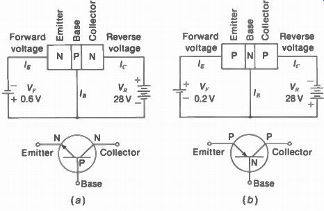
FIGURE 7-14 ELECTRODES AND SYM BOLS FOR JUNCTION TRANSISTORS. (a) NPN, USING
Si WITH FORWARD BIAS OF 0.6 V. (b) PNP, USING Ge WITH FORWARD BIAS OF 0.2
V.
PNP and NPN junction transistors. As shown in Fig. 7-14, three sections or electrodes are used to form two junctions. Either a P is between two N sections, or the N is between two P sections. With two junctions one can control the current through the other to provide amplification of the input signal. This junction type is also called a bipolar transistor because it uses both electrons and hole charges. The three electrodes are called emitter, base, and collector.
The base section is in the middle.
The function of the emitter is to supply charges, either electrons or holes. through its junction with the base. As the source of charges, the emitter function is like the cathode of a vacuum tube. The collector receives these charges through its junction with the base. This function is similar to the plate or anode of a tube, but the collector is positive for NPN transistors or negative for PNP transistors. The base is part of both junctions, to control how many charges can move from the emitter, through the base, to the collector. The function of the base is similar to the control grid in a tube.
Referring to Fig. 7-14, the requirements for electrode voltages in a junction transistor can be summarized as follows:
1. The emitter-base junction must have for ward voltage to bias the transistor into conduction. For a class A amplifier, the forward bias is approximately 0.2 V for all Ge transistors or 0.6 V for all Si transistors. Zero voltage from emitter to base means no forward bias. Then the transistor is cut off, without any output current in the collector circuit.
2. The collector-base junction always has re verse voltage. This polarity is necessary to prevent easy current in the direction from collector to base. Actually, though, the reverse voltage at the collector is the right polarity to attract charges in the base sup plied by the emitter. The amount of reverse collector voltage is about 3 to 20 V for small, signal transistors and up to 200 V for power transistors.
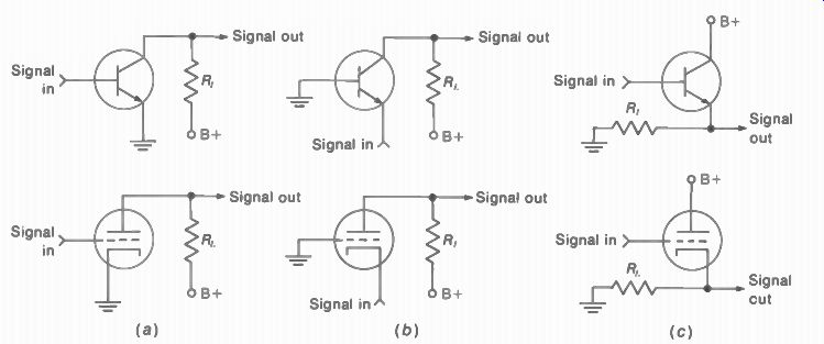
FIGURE 7-15 TRANSISTOR AMPLIFIERS AND THEIR CORRESPONDING VACUUM TUBE CIRCUITS
NPN TRANSISTORS SHOWN (a) COMMON-EMITTER ICE) AND GROUNDED CATHODE (b) COMMON-BASE
(CB) AND GROUNDED GRID. (c) COMMON-COLLECTOR (CC) OR EMITTER-FOLLOWER AND
CATHODE-FOLLOWER
In comparing the operation of tubes with transistors, a tube conducts with plate voltage applied when the negative control grid bias is less than cutoff. However, a transistor must be made to conduct by applying forward bias. This corresponds to heating the cathode in order to produce the charges needed for conduction.
Transistor circuits. With three electrodes for a PNP or NPN transistor there are three possible circuit configurations. These depend on which electrode is used as a common terminal for the input and output signals. The circuits are:
1. Common-emitter (CE): input to the base and output from the collector (Fig. 7-15a)
2. Common-base (CB): input to the emitter and output from the collector (Fig. 7-15b)
3. Common-collector (CC): input to the base and output from the emitter (Fig. 7-15c)
Note that in all the amplifiers, the electrode for signal output has the load resistance R,. Also, the common terminal is shown grounded, but this can be just a common return connection without chassis ground. Further more, the ground return need not be a dc connection. A bypass capacitor can provide an ac ground for signal, even when the electrode has a dc potential. The circuit is named for the common electrode, which is the one that does not have any input or output signal voltage.
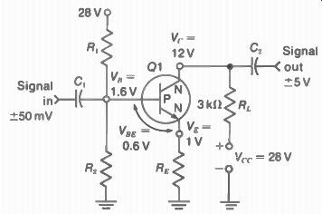
FIGURE 7-16 TYPICAL COMMON-EMITTER (CE) AMPLIFIER CIRCUIT.
The common-emitter circuit is the one used generally for amplifiers. It has the best combination of voltage gain and current gain.
The common-collector circuit is called an emitter-follower, corresponding to the cathode follower circuit with vacuum tubes. This circuit is used for impedance matching because of its high input resistance and low output resistance.
The voltage gain is less than 1, but the stage has current gain. Two emitter-followers in cascade are called a Darlington pair. The two stages are usually dc-coupled and packaged in one unit.
Figure 7-16 shows more details of the CE circuit, using a silicon NPN transistor. The positive 28-V supply is used for reverse voltage on the N collector. R, is the collector load The collector voltage V _p is 12 V because the I_c R_L voltage drop is 16 V. In the base circuit, R1 and R2 form a voltage divider to supply positive forward bias. In the emitter leg, R_E has a voltage drop of 1-V produced by I_E. The net base-emitter bias is 1.6 - 1.0 = 0.6 V for the Si transistor, positive at the P base.
The emitter resistance RE is used to stabilize the CE amplifier against thermal runaway, where I can become excessive if the forward bias is increased because of reverse leakage current. Note that the common terminal for input and output signals is the emitter, al though it is not directly grounded.
The signal input is applied to the base in the CE stage, with amplified voltage output from the collector. With an R, of 3 k-O, a typical voltage gain is 100. The input resistance of the CE stage is 1 1(12 with an output resistance of 50 k-O, approximately. The amplified output signal voltage has inverted polarity, compared with the input. The CB and CC circuits do not invert the polarity.
Field-effect transistor (FET). Field-effect transistors are used as amplifiers, like junction transistors, but the FET construction is different.
The purpose is to eliminate the problems of low input resistance with forward bias and leakage current from reverse collector voltage. The FET provides very high input resistance, in megohms.
Also, the FET can take input signal in the order of volts, compared with less than 0.1 V for junction transistors.
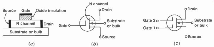
FIGURE 7-17 FIELD-EFFECT TRANSISTOR (FET) WITH INSULATED GATE. (a) CONSTRUCTION.
(b) SYMBOL. (c) DOUBLE-GATE.
In Fig. 7-17, the bulk or substrate material is neutral or lightly doped. This part only serves as a platform on which the channel and gate electrodes are diffused. The source and drain are just ohmic connections at opposite ends of the channel. When voltage is applied between the drain and source, the current through the channel is controlled by the gate electrode. The channel can be either N-type or P-type, but current flows only from source to drain. The FET is a unipolar device, as the charge carriers in the conducting path through the channel have only one polarity. In summary, the FET electrodes are as follows:
Source. The source is the terminal where charge carriers enter the channel bar to provide current. The source corresponds to the emitter. The substrate is usually connected internally to the source.
Drain. This is the terminal where current leaves the channel. The drain corresponds to the collector.
Gate. This electrode controls the conductance of the channel to vary the current from source to drain. Input signal voltage is usually applied to the gate. This corresponds to the base.
In a FET, gate voltage controls the electric field in the channel, while base current controls the collector current in a bipolar transistor. Actually, the gate function is more similar to the control grid in a vacuum tube. These comparisons of junction transistors, field-effect transistors, and vacuum tube amplifiers are listed in Table 7-4.
The FET in Fig. 7-17 is the insulated-gate (IGFET) type, with one gate in b or dual gates in c. This is also called a metal-oxide semiconductor FET, or MOSFET. When the channel can conduct with zero gate bias, the FET is the depletion type. The enhancement type requires a gate bias of about 3 V. In schematic symbols, the depletion type has a solid channel bar, as in Fig. 7-17. For the enhancement type the channel line is shown broken by the D, B, and S electrodes. Another type is the JFET, which uses a PN junction with reverse bias for the gate electrode. The insulated-gate types of FET require a metal shorting ring for the gate while it is out of the circuit, in order to prevent accumulation of static charge. Or, they may have internal protective diodes.
------------------------
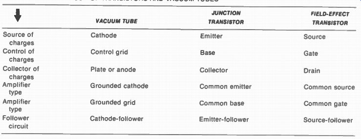
TABLE 7-4 COMPARISON OF TRANSISTORS AND VACUUM TUBES
Source of charges
Control of charges
Collector of charges
Amplifier type
Amplifier type
Follower circuit
VACUUM TUBE
Cathode Control grid Plate or anode Grounded cathode Grounded grid Cathode-follower
JUNCTION TRANSISTOR
Emitter Base Collector Common emitter Common base Emitter-follower
FIELD-EFFECT TRANSISTOR Source Gate Drain Common source Common gate Source-follower
-------------------------
Transistor characteristics. For junction transistors, the ratio I_c/I_B is called beta ( (3) . As an example, with an I_c. of 50 mA and I_B of 1 mA, the beta is 50/1 = 50. Typical values of /I are 20 to 200. The beta value is the current amplification factor in the common-emitter circuit.
For the common-base circuit, the ratio I_O/I_E is used, which is alpha (a). As an example with an I_C of 50 mA and an I of 51 mA, the alpha is 50/51= 0.98. Alpha is always less than 1 because 4. must be less than /E. For field-effect transistors, g„, is the mutual transconductance between gate and drain, defined as I_D/ E_G. As an example, with a drain current of 6 mA and gate voltage of 1 V, the g_m is 6 V/1 mA = 0.006 mho or 6,000 µmhos.
These values of Beta, alpha, and g_m, are static or dc values. When small changes in i or e are considered for signal variations, the characteristics are dynamic or ac values.
FIGURE 7-18 SILICON CONTROLLED RECTIFIER OR SCR (a) CONSTRUCTION. (b) SYMBOL.
FIGURE 7-20 DIAC. (a) CONSTRUCTION. (b) SYMBOL.
FIGURE 7-19 TRIAC. (a) CONSTRUCTION. (b) SYMBOL.
Type numbers. PNP and NPN triode transistors are numbered 2N, as in 2N1613. The "N" is for a semiconductor, and the prefix number 2 is the number of junctions used. Semiconductor diodes are numbered 1N, as in 1N4785. Field-effect transistors are numbered 3N, as in 3N128.
This system is for semiconductors registered with the EIA. Foreign transistors are often numbered 2SA for PNP or 2SC for NPN types. A rectifier stack with diodes in series may have the prefix "CR" as in CR4.
Small-signal transistors are rated at 150 mW, with collector current of 1 mA, approximately. These are practically all silicon, NPN transistors, in a plastic case. Power transistors, rated at 1, 5, 25 W, or more, are often silicon NPN or germanium PNP. These are in a metal case, or the plastic case has a metal heat sink connected to the collector to radiate heat. With a metal case, the collector is usually connected internally to the case to dissipate heat. When the collector is not at chassis ground potential, a mica insulating washer must be used. This washer is coated with a thermal grease for better heat transfer.
Remember that all Si junction transistors, large or small, take a typical forward bias of 0.6 V with 0.2 V used for Ge. The ac signal swing is ± - 0.1 V or less. Small transistors are often soldered into the socket instead of using a socket.
The reason is that oxidation at the socket connections can affect the very small base-emitter voltage.
Silicon controlled rectifier (SCR). As shown in Fig. 7-18, the SCR is a four-layer device used as a silicon rectifier. However, the start of conduction is controlled by a gate electrode. When forward voltage is applied between cathode and anode, in series with an external load, no appreciable load current can flow until the barrier voltage at the gate-cathode junction is over come. This internal reverse bias at the gate is about 0.7 V.
FIGURE 7-21 UNIJUNCTION TRANSISTOR (UJT). (a) CONSTRUCTION (b) SYMBOL
Thyristors. This is the general name for semi conductors that are controlled rectifiers like the SCR. The characteristics are similar to thyratron gas tubes. The main types of thyristors are the SCR, triac, diac, and unijunction transistor (UJT). The SCR and triac are specific types in the general class of four-layer devices that can serve as gate-controlled switches (GCS). As shown in Fig. 7-19, the triac construction enables the thyristor to conduct for either polarity of load voltage in the main circuit. Also, the gate can trigger the triac for positive or negative voltage. The diac in Fig. 7-20 is also bidirectional, but it does not have a gate. In many applications the diac is used to provide pulses for triggering a triac. The unijunction transistor in Fig. 7-21 is a bipolar PNP transistor but with two connections to the base. One of the base connections is used as a gate trigger.
Semiconductor diode rectifiers. A diode is just a PN junction. Since it conducts only in one direction, the diode is a simple, efficient rectifier.
Generally Si is used for power-supply rectifiers, with Ge for signal detectors. A detector is just a low-power rectifier circuit for a few volts of ac signal. Additional types of solid-state diodes include copper oxide and selenium used as metallic rectifiers.
[Named after C. A. Zener, a physicist who analyzed voltage breakdown of insulators. ]
FIGURE 7-22 SEMICONDUCTOR DIODE REC TIFIER. (a) CIRCUIT. (b) TYPICAL DIODES.
AC TUAL SIZE. PELLET AT LEFT. HIGH-HAT AND TUBULAR TYPES. RATED 3A AND PIV
OF 1,000 V.
The standard symbol for a semiconductor diode is a bar and arrow for the PN junction, showing the direction of hole current (Fig. 7-22). This symbol is often marked on the diode.
If not, a dot, band, or any mark at one end indicates the cathode side.
Zener diodes. These are silicon diodes de signed for a specific value of reverse breakdown voltage, which is generally 3.9 V to 27 V. Heavy doping is used to allow appreciable reverse current. For the zener breakdown voltage and a wide range of higher voltages, the reverse voltage across the diode remains relatively constant at the zener value. This characteristic makes the diode useful as a voltage regulator. Zener diodes are also called voltage-reference diodes and avalanche diodes, as the relatively large reverse current can be considered an avalanche current. The diode is not damaged, however, assuming the reverse current is within the power rating.
FIGURE 7-23 CIRCUIT WITH ZENER DIODE TO STABILIZE OUTPUT VOLTAGE ACROSS R,.
FIGURE 7-24 CIRCUIT WITH VARACTOR DIODE TO TUNE RF OSCILLATOR TO 113 MHz.
FIGURE 7-25 INTEGRATED CIRCUIT. (a) CONSTRUCTION. (b) SCHEMATIC. (c) SYMBOL
FOR /C AMPLIFIER UNIT.
Since the diode is a PN junction, reverse voltage is applied as positive voltage at Me N cathode side. The reverse characteristic is used because higher voltages can be applied, compared with forward voltage.
Figure 7-23 shows a voltage regulator circuit with the zener diode to maintain a constant 12-V output across the load R1. The dc input volt- age of 14 to 20V is enough to keep the zener diode in conduction. The series resistance R, limits the current to values within the power rating. Note that the polarity of the input is positive at the N side of the diode for reverse voltage.
Since the diode is in parallel with R1, the voltage across both is constant at 12 V. Varactor diodes. A PN junction with reverse bias is actually a capacitor. The P and N electrodes are the two conductor plates, on both sides of the depletion zone within the junction.
This area serves as an insulator because it has no free charges. C may be 20 pF with reverse bias of 4 V, for typical values. Most important, C changes with the amount of reverse bias. Semi conductor diodes made for this application of a variable capacitance controlled by a dc voltage are varactors or varicaps. The varactor capacitance decreases with more reverse voltage.
The block diagram in Fig. 7-24 illustrates how the varactor is used for electronic tuning.
As part of the LC circuit, the varactor capacitance C,- tunes the rf oscillator to resonance at 113 MHz. However, when C, is varied by controlling its reverse voltage, the oscillator frequency changes.
Integrated circuit (IC). Transistor chips are small, but their use as discrete components with separate resistors, capacitors, and inductors makes the complete circuit relatively large. As an IC example, Fig. 7-25 shows a transistor, resistor, and capacitor on a single wafer. Inductors are not integrated because they take too much space. Transistors and diodes are the easiest components to integrate. Resistors are not precise, but the circuits are designed to depend on ratios of resistances rather than absolute values. Field-effect transistors also are easily integrated.
FIGURE 7-26 PIN CONNECTIONS FOR /C PACKAGES. DOT AT PIN 1. (a) 16-PIN DIP.
THIS IS TO-116 CASE. (b) 10-PIN TO-5. (c) 10-PIN CERAMIC FLAT PACK. THIS IS
TO-91 CASE.
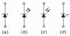
FIGURE 7-27 SCHEMATIC SYMBOLS FOR (a) -UNNEL DIODE; (b) LIGHT-EMITTING DIODE
(LED), (c) PHOTOSENSITIVE DIODE; (d) TEMPERATURE-SENSITIVE DIODE.
In Fig. 7-25a, the layers at the left form an NPN transistor. Note that the collector has a reverse NP junction with the wafer to isolate the transistor. In the middle section, the resistance between the two ohmic contacts of the P material is determined by the length and width of the strip. Cat the right is the capacitance across the reverse-biased junction of the N material to the P wafer. Some areas may need very heavy doping, indicated as N+ or P1-. The schematic diagram of this integrated circuit is shown in b, while the symbol in c is the general form for an IC amplifier.
Three popular types of IC packages are shown in Fig. 7-26. Common applications in the television receiver include the picture IF amplifier section with video detector, 4.5-MHz sound IF amplifier with FM audio detector, and 3.58-MHz chroma amplifier with color demodulators.
Special diodes. Schematic symbols are shown in Fig. 7-27 for additional types of semi conductor diodes. In a is the tunnel diode, or Esaki diode, named after the man who discovered that heavy doping can cause a tunneling effect of charge carriers through the depletion zone at the junction. Because of its negative resistance characteristic, the tunnel diode can be used as an amplifier or oscillator at micro wave frequencies.
The light-emitting diode (LED) in b radiates light when forward voltage is applied. For greater efficiency, special materials such as gallium arsenide are used. Since the diodes are very small, they can be arranged to display numbers and letters. The experimental flat "wall screen," instead of a picture tube, is made of hg it-emitter diodes.
The photoconductive diode in c is made of a photosensitive material, such as cadmium sulfide. Its resistance decreases with more light.
The applications include many light-control devices, including automatic control of brightness in the television picture according to the ambient light in the room.
Two additional diodes without special symbols are the hot-carrier diode and compensating diodes. These have compensating temperature characteristics for bias stabilization in transistor circuits. The hot-carrier diode uses a metal-to-semiconductor junction, such as cop- per to N-silicon. This is used as a signal diode rectifier with better high-frequency response than conventional diodes. One possible application is the video detector.
Protective devices. These include varistors and thermistors. A thermistor (Fig. 7-28a) decreases its resistance with temperature. A varistor (Fig. 7-28b and c) decreases its resistance with higher voltage. The varistor is also called a voltage-dependent resistor (VDR). The collector often has a varistor to protect against voltage pulses that have too much amplitude. As an example, a varistor rated for 70-V peak value can clamp voltage spikes at this value, in either polarity. Also, a diode rectifier can be connected in the collector circuit to isolate the wrong polarity of collector voltage caused by transient voltage surges.
7-9 Special Components
The following list includes special types of capacitors and inductors often used in television receivers.
Ferrite beads. As shown in Fig. 7-29, a bare wire is used as a string for one or more ferrite beads. The wire may be a connection between terminals or one lead from a component. A ferrite is a ceramic material that is magnetic like iron, but the ferrites are insulators. They are generally used for the core in IF and rf coils because the high resistance reduces eddy currents. A ferrite bead on a wire serves as a simple, economical rf choke. The dc resistance is zero because there is no coil. Also, there is no radiation. The ferrite beads are also considered as noise suppressors or inductance multipliers.
They are commonly used in the heater line with tubes, or in the rf, IF, and video circuits for decoupling, shielding, and suppression of parasitic oscillations. As a typical value, a single bead on a 1-in, length of No. 22 wire has an inductance of 300 uH at 100 MHz.
Spark-gap capacitors. These combine the functions of a bypass capacitor and spark gap.
They are generally used at the electrodes of a color picture tube, especially in transistorized receivers. The purpose of the spark gap is to bypass any arc produced in the picture tube, to prevent damage to the transistor amplifiers by voltage surges. The gap capacitor or snap capacitor is often constructed as a flat ceramic with a slit at the top for the spark gap.
Neon bulbs. As a gas tube, a neon bulb has high resistance until the striking voltage of about 90 V ionizes the bulb to make it a short circuit. Therefore, a neon bulb can also be used as a spark-gap protective device for the picture tube electrodes.
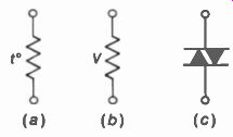
FIGURE 7-28 SCHEMATIC SYMBOLS FOR (a) THERM'S TOR, (b) SILICON CARBIDE VARISTOR;
(c) DUAL-DIODE SILI CON VARISTOR.
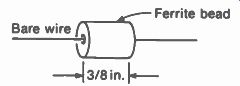
FIGURE 7-29 FERRITE BEAD USED AS RF CHOKE
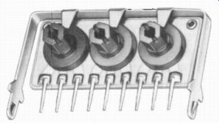
FIGURE 7-30 SET OF THREE VARIABLE RESISTORS FOR SETUP CONTROLS ON PRINTED-WIRING
BOARD. HEIGHT IS "I, IN. (CENTRALAB)
Bipolar electrolytic capacitors. This type consists of two electrolytics connected internally in series-opposition. Then the bipolar capacitor can be used in either polarity. However, the capacitance is cut one-half.
Electrolytic filter capacitors. For transistors, the filter capacitance is usually very high, with a low dc working voltage, compared with tube type receivers. Typical values are 500 to 2,000µF, at 50 V. Electrolytic coupling capacitors. In audio and video circuits, for good low-frequency response, transistor amplifiers use 5- to 10-µF electrolytic capacitors. Large values of capacitors are needed with low resistance.
7-10 Printed-Wiring Boards
Whether tubes or transistors are used, all receivers now have printed wiring, instead of the old hand-wired method with individual solder connections. The components are inserted by machine into small metal holes or "eyelets," and all connections are made at once by dip-soldering. Figure 7-30 shows variable resistors with leads that fit into the eyelet connections.
Some components have metal prongs about 1 in. long, which are used for wire wraparound connections. This arrangement is called a stake. It provides a convenient point for connecting test equipment to the board.
Smaller boards for individual circuits are called modules. These have pin connections that plug into the main chassis, or spring clips, to hold the board in place. The board must be tight. Sometimes oxidation of the contacts causes intermittent connections. If it is necessary, the entire board can easily be replaced.
The following techniques can be helpful when working on a printed board:
1. Use a small soldering iron, of about 25 W, to prevent heat from lifting the printed wiring off the board or loosening the eyelet connections.
2. With IC units, a very thin tip is needed because of the close spacing of pins. You can wrap a piece of No. 12 wire around the tip of the iron and use the wire tip.
3. When soldering a semiconductor component, hold the lead with long-nose pliers, or connect an alligator clip. This conducts heat away to prevent damage to the junction.
4. When soldering field-effect transistors, the leads and the soldering iron should be grounded. The reason is that the gate electrode can accumulate static charge.
5. Resistors and capacitors can often be re placed without disturbing the printed wiring.
Just break the old component in the middle, with diagonal-cutting pliers. Then solder the new component to the old leads.
6. A crack in the printed wiring can be repaired by soldering a piece of bare wire over the open.
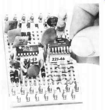
FIGURE 7-31 MODULE BOARD FOR COLOR DEMODULA TOR CIRCUITS WIDTH IS 3 IN (ZENITH
RADIO CORPORAtion )
7. If a larger section of printed wiring is dam aged, you can bridge the open with a length of hookup wire soldered at two convenient end terminals.
8. You can see the printed wiring more clearly by placing a bright light at one side of the board and looking through the opposite side.
To remove components from the eyelet connections, either of the following methods is generally used, working from the printed side of the board: (1) Use a "solder sucker" tool, which acts as a vacuum to pull up the solder after it is melted. (2) Use a piece of wire braid, such as a grounding strap, to pull up the molten solder by capillary action. Some solder paste on the braid helps attract the solder.
The de-soldered eyelet connections must be cleaned of all solder so that the component practically falls out. Otherwise, the printed wiring can be damaged in removing the component.
When any semiconductor board, module, IC, or transistor is moved in or out of its socket, the power should be off. Also, discharge the dc voltage supply. These precautions are necessary because a transient pulse of voltage produced by the circuit change can damage the semiconductor. A typical module board is shown in Fig. 7-31.
7-11 Localizing Receiver Troubles to One Section
We can use four indicators: the sound, raster, picture, and color in the picture for color receivers. Several examples are now analyzed to illustrate how the receiver itself indicates where the trouble is. These troubles are based on the block diagram in Fig. 7-2 for a monochrome receiver.
No raster, with normal sound. Since the sound is normal, the receiver has ac power input, and the low-voltage supply is operating. Assuming that the heater of the picture tube is lit, the trouble of no brightness is usually the result of no anode voltage from the high-voltage supply.
Remember that the horizontal deflection circuits must be operating to produce flyback high voltage.
No picture and no sound, with normal raster. This trouble is in the signal circuits, before the sound takeoff point, because both the picture and sound are affected. The circuits common to the picture and sound signals are the rf section, IF amplifier, second detector, and AGC circuit.
It is useful to see if there is snow in the raster. Snow is receiver noise generated in the mixer stage. No picture with a snowy raster indicates the trouble is in the rf amplifier or antenna circuits, as the snow from the mixer stage is coming through.
No picture, with normal raster and normal sound. In the signal circuits, all the stages operating on the sound signal must be normal.
The one section in Fig. 7-2 operating only on signal for the picture tube is the video amplifier.
Therefore, the trouble must be in this stage.
No sound, with normal raster and normal picture. The trouble must be in the sound circuits, after the sound takeoff point, because only the sound is affected. This includes the 4.5-MHz sound takeoff circuit, the4.5-MHz sound IF amplifier, the 4.5-MHz FM detector, the audio amplifier, and the loudspeaker.
Only a horizontal line on the screen. The horizontal deflection circuits are producing the horizontal line on the picture tube screen and high voltage for brightness. Only vertical deflection is missing. Therefore, the trouble must be in the vertical deflection section of the raster circuits, which includes the vertical deflection oscillator and the vertical output stage.
No raster and no sound. The screen is completely black, without illumination, and there is no sound. This trouble means the raster circuits and signal circuits are not operating. The defect is likely to be in the low-voltage power supply, since this section affects both the raster and the signal.
A common trouble is an open heater in a series string.
7-12 Multiple Troubles
Usually only one defect occurs at a time, but the circuit arrangement can cause multiple effects.
The most common examples are series heaters, multiple tubes, flyback high voltage, a common voltage supply, and the AGC circuit.
Series heaters. When the tube heaters ale in a series string, an open in any one heater means that none of the tubes in the string can light. If the receiver has all tubes in one string, the receiver will be completely dead, without any raster, picture, or sound because all the tubes are cold, including the picture tube.
Multiple tubes. As an example, the pentode section of the 6AN8 may be a common IF amplifier, while the triode is used for the vertical oscillator. Then an open heater in this 6AN8 results in no vertical deflection and no picture or sound.
Common dc voltage lines. In many receivers, the picture IF amplifier tubes obtain plate supply voltage through the audio output stage. In effect, the IF section is in series with the audio amplifier for dc supply voltage. As a result, the audio output stage affects the IF amplifier. If the audio tube does not conduct, there will be no supply voltage for the IF section, resulting in no picture and no sound.
Another example of stages related for dc voltage often occurs in hybrid receivers. In these circuits, the transistor amplifiers can obtain the collector supply voltage of about 12 V from the control grid or cathode of the horizontal output tube.
AGC troubles. The AGC circuit affects both picture and sound by controlling the bias of the rf and picture IF amplifiers. When an AGC amplifier tube is used, the AGC trouble can produce a reversed picture, out of sync, with buzz in the sound, caused by overload distortion.
7-13 Safety Features
In all television receivers the ac line cord is disconnected when the back cover is removed. To operate the receiver with the back cover off, a "cheater cord" is used to fit the male socket on the chassis. The ac-dc type of receiver has a polarized line plug, where the large prong connects to the grounded side of the ac power line.
This requires the polarized type of a cheater cord.
To check which side of the outlet is grounded, you can use a neon-bulb tester or ac voltmeter. From the low side of the outlet to any metal path to earth ground, the ac voltage should be zero, and the neon bulb does not light.
The capacitor of about 0.04 uF as an rf filter across the ac power line is a special non-shorting type. This capacitor should not be replaced with a conventional capacitor.
In addition to the ac interlock for the back cover, the B supply is usually opened when the yoke plug or convergence plug is disconnected.
When servicing a receiver that is not isolated from the power line, it is important to use an isolation transformer. This safety feature prevents a possible short circuit when using line-connected test equipment on the receiver.
The fuses in a television receiver are designed to prevent fire hazard. Do not use larger values and never jump a fuse. Fusible resistors are designed to open with excessive current. These should not be replaced by a conventional resistor. When you are changing wire-fuse links, the replacement must be the exact gage number and length or else the wire fuse will not have the same current rating. A wire-fuse link is often in a sleeve of insulating tubing to catch any drippings, should the fuse melt with an overload. For wired-in fuses, do not mount clips on top for a replacement fuse, as the added weight can move the connections to cause a short circuit.
The high-voltage rectifier for anode voltage is usually in a metal cage as protection against shock hazard and x-radiation. The cover should always be replaced after working in the cage. In some receivers the high-voltage connection to the top cap of the rectifier is open unless the shield cover is in place.
All the metal shields or fish-paper insulators should be in place. The metal shields reduce radiation of signal frequencies between circuits in the receiver, to prevent interference in the picture.
Besides insulation, the fish-paper separators help reduce x-radiation.
The lead dress should be kept the same for several reasons. High-voltage leads must be placed to prevent arcing. Leads with high frequency signals can produce feedback or crosstalk that causes interference in the picture.
In some cases the leads to the picture tube are dressed with specific spacings to serve as spark gap protection. Always make sure that no wire is touching a hot component, such as a power tube, where the lead may become hot enough to burn.
HEW* requires that the receiver not be able to produce a viewable picture when the anode voltage for the picture tube may produce x-radiation. In some receivers, the horizontal oscillator is disabled, resulting in no brightness, when the high voltage exceeds the limiting value of approximately 25 kV. Or, the horizontal synchronization may be removed to produce a picture that is torn apart in diagonal segments.
For ac-dc receivers without a power transformer, the following procedures are recommended to test for leakage current that can cause a shock hazard at exposed metal parts of the receiver.
Leakage current cold check. Disconnect plug from outlet and place a jumper across the two prongs. Turn the receiver switch on. Use an ohmmeter to check from the shorted plug to exposed metal parts such as the antenna handle, control shafts, and metal overlays and mounting screws. Any exposed metal parts that have a return path to chassis should read 2.2 to 3.3 Ma Those parts without a return path to chassis should read infinite ohms for an open circuit.
U.S. Department of Health. Education. and Welfare.
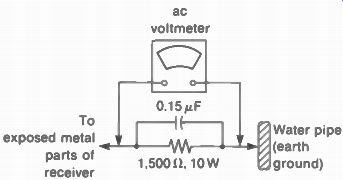
FIGURE 7-32 CONNECTIONS FOR TESTING LEAKAGE CURRENT FROM AC LINE ON RECEIVER
WITHOUT A POWER TRANSFORMER
Leakage current hot check. Plug line cord into ac outlet and turn receiver on. Connect a 1,500-ohm resistor and 0.15-uF capacitor in parallel as shown in Fig. 7-32. Using long clip leads, put this combination in series between earth ground and exposed metal parts of the receiver.
Measure the ac voltage across the RC combination. Do this with the ac plug connected in both polarities, if the plug is not polarized. The ac voltage measured across R and C must not exceed 0.35 V, rms value. Use a portable volt meter, not plugged into the power line.
-----------------

TABLE 7-5 FUNCTIONS OF STAGES IN THE TELEVISION RECEIVER
STAGE VHF rf amplifier VHF rf local oscillator VHF mixer UHF rf local oscillator UHF mixer Picture IF or video IF section Video detector Sound IF amplifier FM sound detector Audio section Video amplifier
INPUT SIGNAL
Rf P and S from antenna None Rf P and S plus VHF oscillator output; or IF P and S from UHF mixer
None Rf P and S from antenna for UHF, plus UHF oscillator output IF P and S from VHF mixer Amplified IF P and S from IF amplifier 4.5-MHz second sound IF signal Amplified 4.5-MHz intercarrier S
Audio signal A from FM detector
Composite video signal from video detector
OUTPUT SIGNAL
Amplified rf P and S for VHF mixer Beats with rf P and S in VHF mixer IF P and S to common IF amplifier Beats with rf P and S in UHF mixer 45.75-MHz P and 41.25-MHz S to VHF tuner as IF amplifier Amplified IF P and S for video detector Composite video signal, 3.58-MHz C, 4.5-MHz S Amplified 4.5-MHz S for FM detector Audio signal to audio amplifier Audio power output 6B for loudspeaker Amplified video signal for picture tube
COMMON TUBES
6CW4 and 6DV4 nuvistor triodes, 6CY5, transistor 6EA8 and 6KZ8 triode-pentodes, transistor 6EA8 and 6KZ8 triode-pentodes, transistor
Transistor
Crystal diode for low noise 6626, 6EH7, 6JH6 pentodes, transistors, or IC Crystal diode 6EH7 or IC 6DT6, crystal diodes, or IC B05, transistors 6CL6, transistors
NOTES
Low noise for no snow
Combined with VHF mixer; tunes 45.75 MHz above P
Converter or first detector on VHF; IF amplifier on UHF
Tunes 45.75 MHz above P Feeds VHF tuner; may have UHF rf amplifier
Two to four stages tuned for 45.75-MHz P and 41.25-MHz S
Picture detector or second detector
Always tuned to 4.5 MHz
Quadrature-grid tube or ratio detector with two diodes
One or two stages
Also Y video amplifier in color receivers
-------
(Continued)
STAGE Sync separator Vertical oscillator Vertical amplifier Horizontal AFC Horizontal oscillator Horizontal amplifier Damper High-voltage rectifier Low-voltage supply
INPUT SIGNAL
Composite video from video amplifier 60-Hz V sync pulses 60-Hz deflection voltage from V oscillator 15,750-Hz H sync pulses Dc control voltage from AFC circuit 15,750-Hz deflection voltage from H oscillator H deflection voltage at 15,750 Hz H flyback pulses at 15.750 Hz stepped up to 15 to 25 kV. Ac power from 120-V main line
OUTPUT SIGNAL
H and V sync for deflection circuits 60-Hz deflection voltage to drive V amplifier 60-Hz sawtooth current in V coils of yoke Dc control voltage for H oscillator 15,750-Hz deflection voltage to drive H amplifier 15,750-Hz sawtooth current in H coils of deflection yoke
Rectified deflection voltage Dc high voltage for anode of picture tube Plate voltage and heater power for tubes: collector or drain voltage for transistors
COMMON TUBES
6BY6. transistor 6DR7 double-triode, or transistors 6DR7 double-triode, or transistors
Two diodes as phase detector 6CG7, 6GH8, or transistors 6D06, 6JE6, power transistor, or SCR 6AU4, 6W4, 6BH3, and 6CT3 diodes, or silicon diode 1B3, 1K3/1J3, 1X2. N 2BJ2, 3A3, and 3CA3 f tubes, or silicon diode Silicon diodes
NOTES
Clips and amplifies deflection sync pulses
Output with or without sync input Often combined with V oscillator Holds H scanning frequency Output with or without dc control voltage Also supplies ac input to HV rectifier and damper Dc output added for boosted B+ voltage Needs H output for operation May be ac supply or transformerless type: heaters may be parallel or series.
---------------
SUMMARY
The functions for all stages in the block diagram of Fig. 7-2 are summarized in Table 7-5. The signal stages are listed first, followed by the raster circuits and power supplies. The double lines across the table indicate separate sections. Note the following abbreviations: P for picture signal, S for sound signal, and /C for integrated circuit. Although 6-V tubes are listed, different heater ratings are used for series strings. The color section is not included, as these circuits are explained in Section 9.
Self-Examination (Answers at back of guide)
Part A
Match the functions listed at the left with the circuits at the right.
1. Anode voltage for CRT
2. Height of raster
3. Width of raster
4. Contrast of picture
5. Brightness of picture
Horizontal amplifier
Video amplifier
Dc bias on picture tube
High-voltage rectifier
Vertical amplifier
Part B:
Match the troubles listed at the left with the circuits at the right, without multiple effects, for the receiver in Fig. 7-2.
1. No picture, no sound, no raster
2. One bright line across center of screen
3. Snowy picture, with good antenna signal
4. No sound, but picture is normal
5. No brightness, but sound is normal
6. Picture in diagonal bars, out of sync
7. No picture, but raster and sound are normal
8. No picture, no sound, but raster is normal
Assume single troubles (a) Vertical oscillator (b) Rf amplifier (c) 4.5-MHz IF amplifier (d) Common IF amplifier (e) Horizontal AFC (f) Low-voltage rectifier (g) Horizontal amplifier (h) Video amplifier Part C:
Match the controls at the left with the functions at the right.
1. Fine tuning
2. Volume
3. Contrast
4. Brightness
5. Station selector (a) Tunes rf, oscillator, and mixer stages (b) Varies frequency of oscillator in tuner (c) Gain or level for audio signal Gain or level for video signal (e) Dc bias for picture tube (d)
Part D:
For semiconductor devices, answer true or false for the following statements.
1. Silicon NPN transistors are generally used for rf and IF amplifiers.
2. Any silicon junction transistor has a forward bias of approximately 0.6 V as a class A amplifier.
3. The collector always has reverse voltage.
4. An NPN transistor takes negative collector voltage for reverse bias.
5. A junction transistor with zero forward bias will not conduct collector current.
6. The common-collector (CC) circuit is similar to a cathode-follower.
7. The field-effect transistor has very low input resistance, compared with junction transistors.
8. Zener diodes are used for voltage regulation.
9. A varactor is a capacitive diode.
10. The drain electrode in the FET corresponds to the plate in a vacuum tube.
Essay Questions
1. Define the following: flyback high voltage, intercarrier sound, monochrome signal, and chrominance signal.
2. State the use for each of the following frequencies: 67.25, 71.75, 45.75, 42.17, 41.25, 4.5, and 3.58 MHz.
3. Give the function of the (a) antenna, (b) transmission line.
4. State the channel numbers tuned in by the (a) VHF tuner, (b) UHF tuner.
5. Give three functions of the composite video signal.
6. What is the advantage of intercarrier sound, compared with split sound?
7. In Fig. 7-2, why is the sync section included in the signal circuits and not in the raster circuits?
8. Using all the stages listed in Table 7-5, classify the stages under the following headings: picture and sound, picture alone, sound alone, synchronization, illuminated raster.
9. List the circuits or stages for the following controls: station selector, fine tuning, contrast, brightness, video peaking, V hold, H hold, AGC level, height, V linearity, width, volume, tone, and buzz.
10. Where would you connect an oscilloscope to see the voltage waveshapes in Fig. 7-33a, b, and c?
11. Give two features of printed-circuit boards.
12. List three safety features of television receivers.
13. Name five types of semiconductor devices, and give their schematic symbols.
14. Define the following: NPN transistor, FET, JFET, IGFET, SCR, triac, zener diode, and varactor.
15. (a) Name the three electrodes in PNP or NPN transistors corresponding to cathode, grid, and plate in a triode tube. (b) Do the same as in a for a field-effect transistor.
16. Draw the circuit of a common-source amplifier with a FET, corresponding to the CE amplifier in Fig. 7-16.
FIGURE 7-33 SEE QUESTION 10
Problems
1. Calculate the oscillator frequencies for tuning in (a) channel 6, (b) channel 7, (c) channel 13, (d) channel 14, (e) channel 83.
2. Calculate the difference frequency in each of the following pairs of frequencies: (a) 83.25 and 87.75 MHz; (b) 175.25 and 179.75 MHz; (c) 45.75 and 41.25 MHz; (d) 83.25 and 86.83 MHz; (e) 45.75 and 42.17 MHz.
3. Draw a block diagram of the monochrome receiver in Fig. 28-14 on a foldout page in Section 28, without the rf tuner unit. Give tube type numbers for each stage.