| Home | Audio mag. | Stereo Review mag. | High Fidelity mag. | AE/AA mag. |
The experimenter who starts using digital ICs faces three basic problems:-
1. How to demonstrate the device in order to understand what it does, the input required, and the output obtained.
2. How to test a new or suspect device.
3. How to power and stimulate an experimental "hook-up" containing one or more digital ICs.
The unit to be described is one possible solution. It is designed mainly to cover the requirements of the TTL range but is generally suitable for other series.
It will be apparent from the foregoing section that an important requirement for the test set is a precise and well regulated power supply. Because accidents can happen, especially with temporary "hook-ups", short circuit protection is also desirable.
A second requirement is some form of logic stimulus as even the most simple logic circuit requires some form of input. A decision has to be made regarding the number of logic outputs to be provided. Circuits to be catered for include gates with 8 inputs, master-slave J-K flip-flops with five, and other circuits with four BCD inputs. After much thought it was decided to provide eight fixed outputs (four "hi" and four "lo") and two outputs which can be switched either "hi" or "lo" . Special design was necessary to ensure that only one logic "hi" and logic "lo" state occurs for every cycle of the switch. This is very important when testing counting circuits.
Finally, the experimenter often wants to know the output state of the circuit under test. In this design one lamp is provided which lights for logic "hi" or "lo" depending on the terminal used. Some constructors may wish to provide additional lamps so that more than one output can be observed at the same time. This would be particularly useful when the device being checked has a BCD output. There is no reason why additional lamp circuits cannot be fitted, except that each lamp dissipates 60 mA when lit, thus limiting the power available to the system under test. Also there is the cost of the extra lamps, holders and driver transistors to be considered. Unlike the input, where stimuli may have to be applied to several points simultaneously, the output state can be checked sequentially.
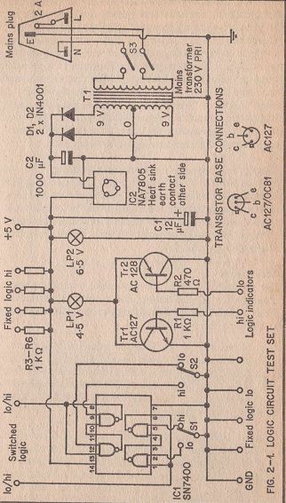
The circuit for the test set is shown in Figure 2-1. It will be seen that the mains is brought in via a fused three pin mains plug and double-pole ON-OFF switch to the primary of the mains transformer. The center tapped 9 - 0 - 9 volt rms secondary drives the full wave rectifier diodes D1 and D2.
An alternative arrangement would be a single 9 volt winding driving a bridge rectifier. Direct current from the rectifier is smoothed by electrolytic capacitor C2 before being fed to the voltage regulator IC2. This little device contains a Zener diode voltage reference, error amplifier, series regulator, and short circuit protection, all in one package. In the event of a short circuit, current overload or overheating, the output voltage falls to nearly zero. The pilot lamp LP2 wired directly across the output of IC2 gives ample warning of something wrong.
Fig. 2-6
Fixed "hi" logic is derived from the 5 V rail via separate current limiting resistors R3, R4, R5 and R6. The earthed or GND rail provides the fixed "lo" logic. Switched logic is taken from the outputs of IC1.
Theoretically it would seem that the switched logic could be taken direct from a simple changeover switch selecting either the 5 volt supply through a current limiting resistor, or "ground" , depending on whether "hi" or "lo" is required.
Unfortunately, even the best quality switches produce electrical noise at the instant of "make" and "break". The characteristic "click" heard in a radio when an electrical switch is operated really consists of many pulses which modem digital circuits respond to. The problem is overcome by using gates wired as bistable multivibrators which immediately latch in favor of the gate selected by the switch. A noisy "make" or "break" has no effect because the circuit remains latched until the switch positively selects the opposite gate. Since there are two pairs of gates in the SN7400 integrated circuit, there are two logic outputs available.
Indicator LP1 operates from both the NPN driver TR1, and PNP driver TR2. To light-up for "hi" , the input is applied via resistor R1 to the base of TR1 which conducts and passes current through the lamp. To light-up for "lo", the input is applied via R2 to TR2 which will also pass current through the lamp. With no input applied to either terminal, the lamp remains extinguished.
Construction
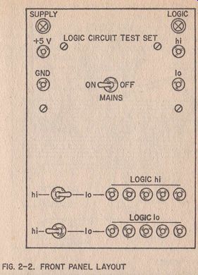
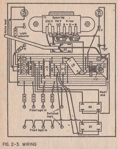
The instrument is housed in a standard aluminum box measuring 7x5x2.5 inches. The layout is illustrated in Figure 2-2, and the internal arrangement including the wiring (not to scale) in Figure 2-3.
It will be seen that the terminals, switches, indicator lamps, mains transformer and circuit board containing the other components, are mounted in the lid which becomes the front panel. The circuit board can be 0.1 inch matrix Veroboard, with copper strips on one side suitably "doctored" , and Veropins fitted as required.
A precise drilling template for the front panel is not given because the dimensions and positions of the holes will depend on the actual components used. Once the holes have been drilled and the burr cleared from the edges, the front panel can be covered with self-adhesive vinyl sheet such as "Contact" or "Fablon". This provides a suitable background
FIG. 2 -2 . FRONT PANEL LAYOUT
FIG. 2-3. WIRING
…for transfer dry-print lettering, such as "Blick" , which may be used for the terminal and switch legends. The lettering should be applied after the components are mounted, and then protected by a coat of varnish. Clear fingernail varnish is ideal.
The voltage regulator IC2 should be fitted with a heat sink made from about VA square inches of 18 gauge metal bent
"U" shape. This is held in place by the same 6BA bolt as that which secures the IC to the circuit board. Examination of the IC will show that metal is exposed on one side, and this should make a firm clean contact with the heat sink. Heat conduction between the two surfaces is improved by the application of a little silicon grease during assembly. The opposite side of the device has three cut-outs surrounding the fixing hole. These are relevant to identifying the connect tags as shown in Figures 2-1 and 2-3.
The wiring is straightforward and should cause no problems but, for safety reasons, it is essential that the conductors carrying mains voltages are well insulated. The writer used plastic covered mains flex for the mains and transformer primary connections, and single-strand plastic-covered tinned-copper wire for the low voltage circuits.
When the wiring is completed the unit may be tested. The 5 volt supply should remain constant to within ± 0.2 volts for loads ranging from zero to 500 milliamperes. This can be checked by applying a suitable 10 ohm load across the terminals. Any sudden fall in output over a reasonably short period is probably due to an insufficient heat sink for IC2. The logic circuits are checked by linking the outputs to the logic indicator input terminals.