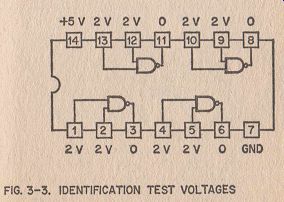
FIG. 3-3 . IDENTIFICATION TEST VOLTAGES
| Home | Audio mag. | Stereo Review mag. | High Fidelity mag. | AE/AA mag. |
The test board shown in Figure 3-1 enables ICs to be rapidly checked using the logic test set just described. It consists of a 16 pin IC holder secured to a small strip of Veroboard which in turn is mounted on a block of wood fitted with terminals.
A 16 pin holder is chosen because it will also accept the 14 pin package, and so cater for nearly all TTL ICs currently available.
Veropins act as soldering posts for the connecting leads which go to terminal strips. The strips used by the writer are obtainable from nearly all chain stores and electrical dealers. They are usually supplied in 12 way strips but can be cut down to 8 way using a small hacksaw. It was found that if the wire gripping screws are slackened off down one side, the strip comfortably "mates" with standard wander-plugs. Consequently, the leads between the board and test-set have plugs at each end in preference to using captive leads with plugs at one end only.
It is proposed to discuss in detail the method of logic-testing.
Manufacturers tests do, of course, cover a much wider range of parameters but these are outside the scope of this guide.
It is often taken for granted that if the logic is correct the other parameters are probably satisfactory. This is not true, but if the logic is correct it is probably worth trying the device under working conditions.
In all cases the specified logic response assumes that the device is correctly powered, with the GND (ground) connections made, and 5 volts applied to the Vcc pin. When the device contains a number of independent circuits, such as the Quad NAND gate type SN7400, each circuit should be checked separately.
TVpe SN7400 in Figure 1 4 is checked by simultaneously applying logic to both inputs of the gate under test and ensuring that the output is in the mode specified by the truth table. That is when both inputs are "hi" the output is "lo". All other input combinations make the output "hi".
Type SN7413 in Figure 1-5 is similarly checked. This time all four inputs must have logic applied. If all inputs are "hi" the output should be "lo". All other input combinations should make the output "hi".
Type SN7476 shown in Figure 1-6 is checked by applying switched logic to the clock input and fixed logic to the J, K, Preset and Clear inputs. The circuit should function in accordance, with the truth table and description given in Section 1. The same applies for the type SN7472 shown in Figure 1-7.
TVpe SN7490 is best checked as follows:-
1. Switched-logic to the divide-by-two input (pin 14).
2. Connect counters in the BCD mode by linking pins 1 and 12.
3. Switched logic (set to "lo") to the reset-to-zero (pin 2).
4. Fixed logic "hi" to pin 3.
5. Reset-to-nine function inhibited by connecting pins 6 and 7 to fixed logic "lo".
6. Refer to the truth table for the BCD mode. The count should be zero. Use the logic indicator "hi" terminal to check outputs A, B, C, D (pins 12, 9, 8,11). These should all be at logic "lo" and the lamp should not light.
7. Set the switched logic going to pin 2 to "lo" to inhibit the reset-to-zero function.
8. Operate the switched logic going to pin 14 through one full cycle. That is from "hi" to "lo" and back to "hi"
9. Check the logic at outputs A, B, C, D. Only "A" should be "hi" and light the lamp (see the truth table for a count of " 1 ").
10. Sequentially cycle the switched logic going to pin 14, and after each cycle check the output logic at A, B, C, D to ensure that results agree with the truth table.
11. Check the reset functions by making pins 2 ,6 ,3 ,7 "hi" and then "lo" in turn. Note that A, B, C, D outputs give BCD readings of 0 ,9 ,0 ,9 .
Type SN74141 in Figure 1-9 is checked by applying fixed logic to the A, B, C, D inputs at pins 3 ,6 ,7 , 4 in the order given by the truth table. In this case the correct output can be ascertained by using the logic indicator "lo" terminal to detect the active output pin.
Identifying Digital ICs
An equivalents chart covering most common TTL codes is given in Figure 3-2. The suffix shown against some first numbers may also apply to other numbers in the same range and simply indicates a dual-in-line package.
Some numbers have the letter "H" following the "74" digits; e.g. SN74H00. The logic is similar but high speed performance is better. Alternatively the letter "L" may be used in the same place to indicate a device dissipating less power than the standard type. Also produced is a range of devices having the digits "54" instead of "74" ; e.g. SN5400. Again the logic is the same as for the SN7400, but this time the specified temperature limits are much wider (-55°C to 125°C) instead of the usual 0°C to 70°C).
Occasionally the experimenter is faced with the almost impossible task of identifying a device having a code which has been defaced or completely obliterated. This can happen in the case of "bargain buys" , manufacturers "throw-outs", or ICs salvaged from old printed circuit boards. With a little detective work and the application of 'logic!!'' it is sometimes possible to identify unmarked digital ICs. Proceed as follows:
1. If the IC has a number or a part of a number, can it be identified from the chart shown in Figure 3-2?
2. Has the supplier marked the IC with a special code which can be identified from an advertisement or data sheet?
3. I f the device was removed from a circuit board, can it be identified by the circuit configuration? This is sometimes possible with easily recognized circuits such as counters.
4. Perhaps the board from which the IC was removed has some legend or marking which will assist identification.
At least the supply connections can be traced because they usually go to common lines. Mark these pins I before removing the IC from the board.
5. How many pins does the IC have? The following statistics were derived from a review of manufacturers datasheets:
14 pin ICs 85% Vcc=pin 14; GND=pin 7; (gates & inverters) 12% Vcc=pin 5; GND=pin 10; (counters etc.) 3% Vcc=pin 4; GND=pin 11; (arithmetic ICs) 16 pin ICs 58% Vcc=pin 16; GND=pin 8; (decoders) 34% Vcc=pin 5; GND=pin 12; (decoders & arithmetic) 8% Vcc=pin 5; GND=pin 13; (SN7476 flip-flop)
FIG. 3-3 . IDENTIFICATION TEST VOLTAGES
6. Try powering the device. Digital ICs are rarely damaged by incorrect power connections unless the voltage limits are exceeded. Does the power dissipated by the IC come within the normally expected range of 4 to 100 mA?
7. With the device powered, use a voltmeter to detect the potential at each pin. I f Vcc or GND connections are incorrect there will either by very low voltage detected at all inputs except that connected to the 5 volt supply, or nearly 5 volts at all pins except that connected to the GND return.
8. If the Vcc and GND connections are correct, the input pins will be approximately 1 to 2 volts, although clock connections to multivibrators and counters can be higher. Outputs will either by "hi" (nearly 5 volts) or "lo" depending on the circuit mode at switch-on.
9. From the data derived from the voltage tests, sketch the base diagram and insert the values and probable base connection. Try to match this with the base connection detail given in data sheets. See Figure 3-3 for an example.
10. Finally, make a full logic check along the lines already discussed. Do not forget to mark the device with the probable code number.
-------
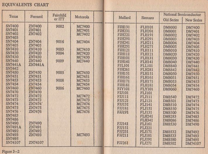
Figure 3-2
EQUIVALENTS CHART
Before throwing out faulty ICs, it is a good idea to check whether any serviceable sections remain. For example, the SN7413 contains two Schmitt-triggered NAND gates; perhaps only one of these circuits is faulty. Partly service
able devices are always handy for experimental work, and it is a good plan to mark them so that the good sections are easily identified. Colored fingernail varnish is ideal for this purpose. It comes in bottles complete with a little brush for immediate use, and quickly dries.