AMAZON multi-meters discounts AMAZON oscilloscope discounts
In Sections 4, 5, and 6, the signals to be detected were amplitude-modulated (AM). In this and the next section, methods of recovering the modulating signal from a frequency-modulated (FM) carrier will be discussed. Since the FM signal differs from the AM signal in the previous sections, a brief discussion of the signals will be given before operation of the discriminator circuit is explained.
THE FM SIGNAL
Fig. 7-1 shows a series of waveforms from which it is possible to derive some essential definitions associated with frequency modulation. Figs. 7-1A and 7-1C are audio-frequency sine waves of voltage which have been used to modulate the carrier waves of Figs. 7-1B and 7-1D. Fig. 7-1A represents an audio voltage of low volume of amplitude (meaning loudness), and Fig. 7-1C, an audio voltage of high volume or amplitude. For simplicity we might assume that the audio frequency in each case is 1,000 cps.
Hence, an individual audio cycle will be 1/1,000th of a second.
The frequency of the carrier wave may be anywhere in the assigned band of frequencies allocated for FM broadcasting. The latter is from 88 to 108 megacycles. This is considerably above the 550-1600-kc band assigned for amplitude-modulation broad casting.
In the waveforms of Fig. 7-1, the carrier varies both above and below an assigned frequency called the center frequency.
When no sound and consequently no modulation are imposed on the carrier at the transmitting end, the carrier frequency will be stabilized at its assigned center frequency. Let us assume this center frequency to be 100 megacycles.
When some audio-modulating voltage is applied to the carrier, its frequency will vary on either side of the center frequency, but will return to the center frequency twice during each audio cycle. This occurs as the audio voltage passes through its own reference line and has a value of zero. These are the moments when the audio voltage is changing its polarity.
The number of cycles or kilocycles by which the carrier deviates from its center frequency is called the frequency deviation.
It is measured from the center frequency to either the highest or the lowest frequency attained by the carrier. The maximum deviation from the center frequency prescribed by regulation for commercial FM broadcasting is 75 kilocycles. Thus, a carrier with an assigned center frequency of 100 megacycles may legally vary, or "deviate," between 99.925 and 100.075 megacycles.
Sound has two distinguishing features-frequency (pitch) and volume (loudness). To be successful, any radio transmitting system must be capable of modulating the radio-frequency wave in such a manner that these two important sound characteristics of pitch and loudness are faithfully reproduced. Fig. 7-1 provides some idea of how this is done in a frequency-modulated carrier.
Audio Amplitude:
The amount in kilocycles by which the carrier deviates from its center frequency is determined by the amplitude of the modulating audio voltage-in other words, by its volume, or loudness.
Two successive whole audio cycles, or four half-cycles, are indicated in Fig. 7-1. At the start of each half-cycle, the audio voltage is neither positive nor negative. Rather, it is passing through zero and the carrier is at its center frequency. In the middle of the first half-cycle, the modulating audio voltage reaches a positive peak.
Accordingly, the carrier frequency will have deviated to a some what higher frequency-perhaps 25 kilocycles above the center frequency, or 100.025 megacycles.
Midway in the second half-cycle, the modulating audio voltage has reached its negative peak and the carrier frequency accordingly will have deviated to a somewhat lower frequency. Only this time the deviation is 25 kilocycles below the center frequency, or 99.975 megacycles.
As stated before, Fig. 7-1A represents the waveform of an audio voltage of low volume, or amplitude. Fig. 7-lC represents the waveform of an audio voltage of the same frequency but with a high volume, or amplitude. Because of this higher volume, the frequency deviations of the carrier will be greater. Midway in the first half-cycle in Fig. 7-1C and 7-1D, the audio voltage reaches its positive peak. At this time the carrier frequency will have deviated 50 kilocycles above the center frequency, to a new frequency of 100.050 megacycles. Midway in the second half of the audio cycle in Figs. 7-1C and 7-1D, the modulating audio voltages reaches its negative peak. Now the carrier will have deviated the same amount of 50 kilocycles below the center frequency, to a new value of 99.950 megacycles.
Fig. 7-1. The relationships between the amplitude and frequency of the
audio signal with the carrier. (A) Low-amplitude audio-modulating voltage.
(B) Carrier resulting from modulation by A. ( C) High-amplitude audio-modulating
voltage. (D) Carrier resulting from modulation by C.
In a properly adjusted modulating system, the frequency deviation should at all times be proportionate to the amplitude of the modulating voltage. Consequently, for a frequency deviation of 50 kilocycles to be achieved as in Fig. 7-1D, versus the deviation of 25 kilocycles achieved in Fig. 7-1B, the modulating audio voltage in Fig. 7-1C would have to have twice the amplitude of the voltage in Fig. 7-1A. Audio Frequency The rate at which the carrier deviates in frequency between its two extremes is determined by the frequency of the modulating audio voltage. This should be fairly evident from Fig. 7-1. During the two audio cycles shown in this figure, the carrier completes two cycles of deviation. From center to maximum frequency, to center and to minimum, and back to the center frequency constitutes one complete cycle. The rate at which the carrier frequency deviates is sometimes called the excursion frequency, and it will always be equal to the frequency of the modulating audio voltage.
THE DE-TUNED DISCRIMINATOR
Figs. 7-2, and 7-4 show a fairly standard discriminator circuit used for demodulating a frequency-modulated carrier wave. Each of these figures depicts a different operating condition for the circuit. Fig. 7-2 shows significant currents and voltages when the circuit is being operated exactly at the center frequency. Fig. 7-3 shows currents and voltages when the carrier frequency has deviated above the center frequency, and Fig. 7-4, when the carrier frequency has deviated below the center frequency.
The circuit components of this type of discriminator circuit are as follows:
R1-Filter resistor for V2.
R2-Filter resistor for V3.
C1-Tank capacitor for final RF- or IF-amplifier stage.
C2-Tank capacitor for "high" deviation tank circuit.
C3-Tank capacitor for "low" deviation tank circuit.
C4-Filter capacitor for V2.
CS-Filter capacitor for V3.
L1-Tank inductor for final amplifier stage.
L2-Tank inductor for "high" deviation tank circuit.
L3-Tank inductor for "low" deviation tank circuit.
V1-Pentode RF- or IF-amplifier tube.
V2 and V3-Diode detector tubes.
Identification of Currents:
Operation of this type of circuit can be understood from a discussion of the following electron currents:
1. Plate current through tube V1 (solid red).
2. Oscillating current in final amplifier tank circuit ( dotted red).
3. Current through first rectifier diode, V2 (solid blue).
4. Oscillating current in upper tuned tank circuit (dotted blue).
5. Current through second diode rectifier tube, V3 (solid green).
6. Oscillating current in lower tuned tank circuit ( dotted green).
7. Radio-frequency filter currents in two filter capacitors, C4 and CS (solid blue and solid green, respectively).
Fig. 7-2. The detuned discriminator-operation at its resonant frequency.
Details of Operation:
The three tank circuits are each tuned to different frequencies.
The first circuit, consisting of L1 and C1, will be tuned exactly to the center frequency. Since frequency conversion undoubtedly has already taken place, the center frequency in the demodulation process will be much lower than the center frequency that exists during transmission and the initial reception. When the carrier initially was received, its center frequency may have been 100 megacycles and the frequency deviations due to modulation may have caused it to vary 75 kilocycles (the maximum allow able) on either side. However, after frequency conversion (called heterodyning) , the new center frequency may be 10 megacycles.
The same frequency deviations will have been preserved, of course. In other words, if the original carrier deviated the full 75 kilocycles-from 100 to 100.075 megacycles-the new IF carrier will also deviate 75 kilocycles, from 10 to 10.075 megacycles.
Assume that tank L1- C1 is tuned to this new center frequency of 10 megacycles. The tank consisting of inductor L2 and capacitor C2 will be tuned to a higher frequency, and the other tank (L3 and C3) will be tuned to a lower frequency. Hence, these two tank circuits are not tuned to the center frequency to which the first tank is tuned. They are said to be detuned and the circuit is named a detuned discriminator.
Fig. 7-3. The detuned discriminator-operation above resonance.
Discriminator Response Curve:
Fig. 7-5 shows a typical frequency-response curve for the aver age discriminator circuit. A response curve is defined as a graphical representation of the response, or output, of the circuit throughout the entire range of frequencies in which the circuit operates. Fig. 7-5 has three essential parts: The response curve of the upper-detector circuit (blue) consists of tank L2-C2, diode V2, load resistor R1, and filter capacitor C4. The response curve of the lower-detector circuit (green) consists of tank L3-C3, diode V3, load resistor R2, and filter capacitor C5. The response curve of the two detector circuits taken together is shown in black. It is desirable for a discriminator to be operated along the linear portion of its overall response curve. (See Fig. 7-5.) The response curve of the whole circuit is merely an algebraic addition of the two individual response curves. On either side of the center frequency, the sum of these two curves gives a fairly straight line, as indicated. As the carrier frequency deviates farther from the center frequency, the response of one of the two diode-rectifier circuits dwindles to the vanishing point. Eventually the total response curve has almost the same shape as the response curve of the other diode.
If the linear portion of the response curve extends, say, 75 kilo cycles on either side of the center frequency, the two detuned peaks must be resonant at frequencies farther removed than this amount from the center frequency. As an example, tank L2-C2 might be tuned 150 kilocycles higher than 10 megacycles, to a resonant frequency of 10.150 megacycles. Tank L3-C3 would then have to be tuned 150 kilocycles lower than the center frequency, or 9.850 megacycles.
Operation at the Center Frequency
Fig. 7-2 shows the significant currents and voltages when this discriminator circuit is being operated at the exact center frequency. The frequency at which this circuit is being operated is of course determined by the carrier frequency. When it is exactly 10 megacycles, ten million pulsations of plate current will pass through amplifier tube V1 each second. (This is the current shown by the solid red line.) Each such pulsation sustains one cycle of oscillation of the electrons which make up the plate-tank current (shown in dotted red). Since both L2 and L3 act as secondary windings in their relationships with L1, the plate tank current will induce a current in each coil. This current in turn will set up and sustain electron oscillations in each of the two tank circuits, L2-C2 and L3-C3.
The upper tank circuit (L2-C2) will be operating below its own resonant frequency, whereas the other will be operating above its own resonant frequency. Nevertheless, the most important result is that the oscillation in each tank is considerably weaker than if each tank were operated at resonance. Further, the two oscillations are reduced equally in strength, so that they remain equal.
(This presupposes that the two diode circuits have identical de signs and degrees of coupling to primary winding L1. Unfortunately, such design objectives are not easily achieved.) Rectification Each diode circuit operates in the manner described in the diode-detector portion of this guide, the only difference being in the placement of the RC filter combination. In that section, the RC filter was located where it could "bias" the diode plate with a negative voltage. In this section, this bias is a positive voltage.
In both cases the bias is the detected voltage.
In the upper-diode circuit, each positive half-cycle will drive the plate of diode V1 to a slightly more positive voltage peak than the cathode. This causes electron current (shown in solid blue)
to cross from cathode to plate, downward through inductor L2, across to the junction with resistor R1, and upward through R1 to the cathode. This is not a continuous current, but an intermit tent one that flows only at the peaks of positive half-cycles of tank voltage. However, the portion that flows through resistor R1 is of course a continuous current, since it is drawn upward by the electron deficiency (positive voltage) on the upper plate of capacitor C4.
The output for the upper-diode circuit is this positive voltage stored on the upper plate of C4. Under the conditions described earlier, it might have a value of + 10 volts when the carrier is exactly on the center frequency. Since the output voltage for the entire circuit is measured across both RI and R2, this portion of the output voltage must be added algebraically to that portion developed independently across R2 by the current through the second diode. The latter will also equal 10 volts, but the bottom of R2 will be positive. Let us see why.
During the peaks of the positive half-cycles of tank voltage in the lower tank circuit, diode V3 will conduct from cathode to plate. These electrons, shown by solid green lines, then flow up ward through inductor L3 to the junction with R2, and downward through R2 to the cathode. Like the current through diode V2, this current is also intermittent except through R3, where it flows continuously towards the cathode.
When we say the voltage at the cathode is a positive 10 volts, we mean of course that it is positive with respect to the voltage at the other end of resistor R2. Since the cathode of V2 has been grounded in this particular circuit, the voltage at the top of R2 must be -10 volts. The voltage at the cathode of the upper diode is + 10 volts with respect to this voltage at the junction of the two resistors, by virtue of the upper-diode current. Hence, the voltage at the cathode of V2, as at the cathode of V3, will have a true value of zero.
Since the voltages at the two diode cathodes both equal zero, the difference between them-which is also the output voltage for the entire circuit-is zero. This is as it should be, and can be con firmed by referring to Fig. 7-1. At those two moments in each cycle when the audio-modulating voltage was passing through the reference line and therefore was equal to zero, the carrier was exactly equal to the center frequency.
Operation:
Above the Center Frequency Fig. 7-3 shows significant currents and voltages when the carrier is higher than the center frequency. Now tuned circuit L2-C2 will be operating more nearly at its own resonant frequency. In accordance with the selectivity or response curve of Fig. 7-5, a stronger oscillation of electrons will be built up in the tank, as indicated by the three dotted-blue lines. Each positive voltage peak which is applied to the plate of diode V2 will be proportionately higher, and more current will flow through the diode. This increases the electron deficiency (positive voltage) on the upper plate of capacitor C4, and of course the amount of current flowing upward through R1. The amount of voltage stored in the capacitor is always the same as developed across the resistor.
Since tuned circuit L3-C3 is tuned lower than the center frequency, in Fig. 7-3 this circuit will be operating even farther from its resonant frequency than in Fig. 7-2. Its response curve from Fig. 7-5 indicates that a comparatively weak oscillation of electrons (indicated by the single dotted-green line) will be in motion in the tank. Consequently, diode V3 will conduct fewer electrons than before. Less current will flow through resistor R2, and less voltage will be developed across it.
Fig. 7-4. The detuned discriminator-operation below resonance.
Since the output voltage of the entire circuit is the algebraic sum of the two separate voltages across R1 and R2, it is obvious that when the circuit is operated above the center frequency, the output voltage at the top of resistor R1 will be positive. The amount of this voltage depends on the amounts of conduction in each diode tube. In turn, these amounts depend on the strength of each electron oscillation in the two tuned tanks, L2-C2 and L3-C3. As the operating frequency moves higher and higher to ward the resonant frequency of tank L2-C2, the amount of voltage developed across R1 increases steadily, whereas the amount across R2 decreases. Consequently, the sum of these two voltages--which is the output of the circuit-is a positive voltage which increases as the carrier frequency does. From Fig. 7-1 we deduce that a positive voltage output is associated with a positive peak in the modulating audio voltage. Also, we see that the output-volt-age peak is directly proportionate in size to the modulating audio voltage.
Operation Below the Center Frequency
Fig. 7-4 shows the important currents and voltages in this circuit when the carrier is below the center frequency. Tuned circuit L3-C3 will now be operating more nearly at its resonant frequency. The oscillation of electrons in that tank becomes stronger, and more current flows through diode V3 and resistor R2. This results in a much greater voltage drop across R2.
At the same time, the oscillation in upper tank L2-C2 will be drastically weakened because it will be operating far from its resonant frequency. The response curve of Fig. 7-5 which applies to this tank indicates a very low response. So only a small current will flow upward through R1 and develop only a small voltage across this resistor. This voltage will be positive at the top of R1.
The output is the sum of the two voltages across R1 and R2.
The junction of these two resistors is at a fairly large negative voltage with respect to ground, by virtue of the larger current flowing through R2. Thus the total output voltage, measured at the top of R1, will also be negative. Again this is consistent with Fig. 7-1, which indicates that a negative audio peak voltage is associated with a lower operating frequency. It is also consistent with Fig. 7-5, which illustrates that a lower operating frequency leads to negative output voltages.
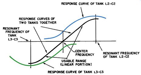
Fig. 7-5. Response curve of the detuned discriminator.
Summary:
From the foregoing discussion it is evident that the output voltage varies from positive to negative at an audio rate which depends on the excursion frequency of the carrier. The latter is of course the same as the frequency of the modulating audio voltage.
Thus the audio frequency has been reproduced by this type of demodulation.
The amplitude of the audio-output voltage depends on how greatly the carrier deviates from the center frequency. A deviation toward a higher frequency causes a positive voltage at the output point, and a deviation toward the lower frequencies causes a negative voltage. In either case the size of the deviation deter mines the size of the output voltage. Since the amount of frequency deviation is controlled by the amplitude of the modulating audio voltage within the transmitter, this discriminator circuit can accurately reproduce the intended audio amplitude as well as frequency.
TUNED DISCRIMINATOR
Figs. 7-6, 7-7, 7-8, and 7-9 represent four quarter-cycles in the operation of a tuned discriminator circuit at the center frequency.
As with the detuned discriminator discussed previously, the function of this circuit is to demodulate a frequency-modulated signal.
Unlike the detuned discriminator, however, two tuned circuits are used instead of three, and the primary and secondary tuned circuits are coupled inductively and capacitively. (The significance of this dual coupling will be discussed later.) The operation of this circuit is somewhat more difficult to visualize than it is for the detuned discriminator.
Identification of Components
The tuned discriminator includes the following necessary circuit components:
R1-Cathode biasing resistor for V1.
R2-0utput resistor for V2.
R3-0utput resistor for V3.
C1-Primary tank tuning capacitor.
C2-Coupling capacitor between two tank circuits.
C3-Secondary tank tuning capacitor.
C4-Filter capacitor for V2.
C5-Filter capacitor for V3.
L1-Primary tank inductor.
L2-Secondary tank inductor.
V1-Final IF amplifier tube, usually a pentode.
V2-Upper-diode detector tube.
V3-Lower-diode detector tube.
Identification of Currents
The following electron currents are at work in this circuit:
1. Plate tank current (solid red).
2. External current driven by plate tank current (dotted red).
3. Secondary tank current (dotted blue).
4. Upper-diode current (solid blue).
5. Lower-diode current (green).
Details of Operation
To understand the operation of this circuit, it is necessary to review its operation on a single-cycle basis at the center frequency, and also above this frequency. Figs. 7-6 through 7-9 show the four successive quarter-cycles of operation at the center frequency, and Fig. 7-10 the significant voltage waveforms during a single cycle.
Operation at the Center Frequency
It is not readily apparent from the circuit diagrams, but inductors L1 and L2 are two halves of a radio-frequency transformer.
Hence, any change in the amount of current flowing through L1 will induce a voltage and a companion current in secondary winding L2. Also, any changes in the voltage at the top of the primary tank circuit simultaneously will be coupled-via capacitor C2 to both sides of the secondary tank and to both detector diodes.
It is a well-established fact that when two tuned circuits are operated exactly at resonance, the two tank voltages will be exactly 90°, or a quarter of a cycle, out of phase. Usually the secondary tank voltage is said to lag the primary tank voltage by a quarter of a cycle-meaning the voltage at the top of the secondary tank circuit will reach its positive peak a quarter of a cycle after the voltage at the top of the primary tank reaches its positive peak.
The resonant frequency of these tank circuits is the center frequency. In the amplifier volume of this series, the section on radio-frequency amplifiers contains a detailed discussion of tuned circuits and their operation in the vicinity of their resonant frequency. The entire discussion will not be repeated here; any readers wishing to learn more about tuned circuits are referred to this volume.
Looking at Fig. 7-10 in conjunction with the four quarter-cycle diagrams, you will see that the voltage across primary tank circuit L1- C1 is positive during the first two quarter-cycles, reaching its peak at the end of the first quarter-cycle. During the last two quarter-cycles, the tank voltage is negative, reaching its peak at the end of the third quarter-cycle. This oscillatory voltage across the primary tank is accompanied by an oscillatory current (red) through it. During the first quarter-cycle (Fig. 7-6), this current flows downward through coil L1 and delivers electrons to the lower plate of tank capacitor C1, leading to a negative peak voltage on the lower plate and a positive one on the upper plate.
During the second quarter-cycle (Fig. 7-7), this tank current reverses and flows upward through the coil. The charge ( electrons) stored in the capacitor is redistributed, taking a half-cycle to do so, and the tank voltage reverses polarity. The voltage at the top of the primary tank reaches its negative peak at the end of the third quarter-cycle (Fig. 7-7) .
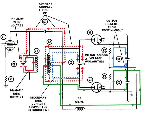
Fig. 7-6. Operation of the tuned discriminator at the center frequency
first quarter-cycle.
The purpose of capacitor C2 is to couple this tank voltage directly to both sides of the secondary tank circuit. This is accomplished by connecting C2 to a center tap on coil L2. The resultant current flow, shown in dotted red lines, flows to the left during the first two quarter-cycles and to the right during the last two.
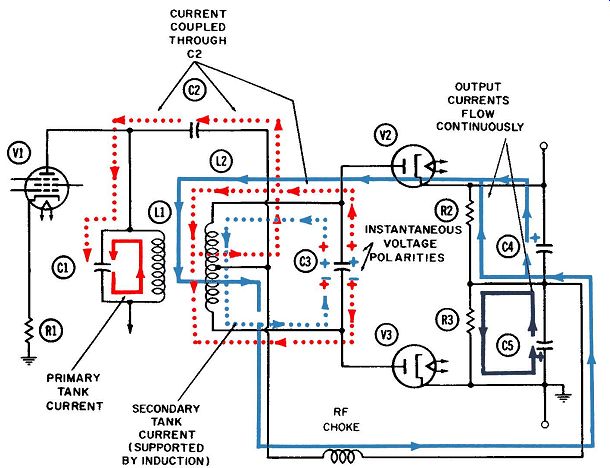
Fig. 7-7. Operation of the tuned discriminator at the center frequency
second quarter-cycle.
Called an "external" current to the oscillation in the primary tank, it constitutes a load on the primary tank oscillation and, like any other loss or load current, should be kept as small as possible.
This current provides the necessary function of simultaneously transferring the polarity of the voltage at the top of the primary tank to both sides of the secondary tank. This positive polarity indicated by the red plus signs on both plates of capacitor C3 during the first two quarter-cycles-results from the fact that the external current from the primary tank is drawing electrons away from both sides of the secondary tank. These electrons, which make up the external current, will continue to be drawn toward the primary tank during the first two quarter-cycles as long as the voltage across the primary tank is positive. During the third and fourth quarter-cycles, the tank voltage across the primary tank circuit has a negative polarity at the top and these electrons will be repelled. This accounts for the red minus signs on both sides of capacitor C3 in Figs. 7-8 and 7-9.
A primary function of coupling capacitor C2 is to isolate-or "block"-the high positive voltage of the power supply connected to the bottom of L1 and C1 from the plates of the two diode detectors. This coupling function can always be performed better by a piece of straight wire than by a capacitor. It should be under stood that neither side of the primary tank ever reaches a true negative voltage; instead, the voltage varies between a low and a high positive value. Thus, on alternate half-cycles, each plate of capacitor C1 is shown as being negative, but actually it is negative only with respect to the other plate.
The oscillating voltage in the secondary tank circuit is supported by induction between L1 and L2. These two coils are in reality two windings of a radio-frequency transformer. Fig. 7-10 indicates that this oscillation of electrons leads to a peak of positive voltage on the upper plate of capacitor C3, and to a peak of negative voltage on the lower plate, at the end of the second quarter-cycle.
To determine the total voltage applied to the plate of the upper diode at any moment, it is necessary to add the amplitudes of the two separate voltages at that point. Since the amplitudes are rep resented by the waveforms labeled A and Bin Fig. 7-10, the sum of the two can be represented by waveform E. Observe that the positive peak of this voltage sine wave occurs midway in the second quarter-cycle-after the peak of coupled voltage but before the peak of oscillatory voltage. This is the moment when upper diode V2 will conduct the most electrons. This diode current (solid blue in Fig. 7-7) flows from cathode to plate within the tube, downward through coil L2 to the center tap, and back through the RF choke to the bottom of resistor R2. From here it flows upward through R2 and returns to the cathode. This current causes a positive voltage at the top of R2, and also on the upper plate of capacitor C4. This positive voltage becomes a portion of the discriminator output voltage. The balance of the output voltage is developed across resistor R3 by the other diode current.
The sine wave (labeled waveform C in Fig. 7-10) represents the amplitude of the oscillatory voltage at the bottom of tuned secondary tank L2-C3. Obviously, this voltage should always be a half-cycle out of phase with the oscillatory voltage at the top of the tank. From waveform C we can observe that the oscillatory voltage at the bottom of the tank reaches its positive peak at the start of the first quarter-cycle.
The total voltage at the bottom of the tank is found by adding waveforms A and C together, giving the waveform labeled E in Fig. 7-10. This voltage reaches its positive peak midway in the first quarter-cycle-after the oscillatory tank-voltage peak but before the voltage peak due to the capacitive coupling from the primary tank circuit. This is the moment when maximum conduction occurs through lower diode V3. The complete path of these electrons is indicated (in green) in Fig. 7-6 only, since this is probably the only quarter-cycle in which the lower diode con ducts at all. The complete path takes the electrons from cathode to plate within the tube, upward through the lower half of coil L2 to the center tap and out, through the common return line to the upper end of R3, then downward through this resistor and back to the cathode. This current flow develops a voltage across R3 which then becomes part of the output voltage. Since the lower end of R3 is connected to ground, the upper end must be more negative. The downward flow of electrons toward the more positive lower end verifies this statement.
The detector output voltage is the algebraic sum of the voltages across output resistors R2 and R3. When the discriminator circuit is operated exactly at resonance-which is the center frequency these two voltages will be equal in value but opposite in sign, so their sum will be zero. Recall that Fig. 7-1 related the modulating audio-voltage waveform to the carrier-frequency waveform. Here you can see that when the modulating audio voltage is crossing its own reference line and is therefore zero, the carrier will be exactly on its center frequency. Thus, when the modulating audio voltage is zero, so is the demodulated ( detected) output voltage.
The Filtering Actions
C4 and C5 act as conventional filter capacitors, in conjunction with output resistors R2 and R3, respectively. When upper diode V2 conducts during the second quarter-cycle, it draws electrons from the upper plate of capacitor C4, making this plate positive (electron deficiency). This positive voltage, which persists throughout the entire cycle, accounts for the continuous upward flow of electron current through R2.
By somewhat analogous reasoning, we can show that the upper plate of C5 assumes a negative voltage by virtue of the electrons delivered there during the first quarter-cycle. The negative voltage on the upper plate of C5 will drive electrons downward through resistor R3 during the entire cycle, as depicted in each quarter-cycle diagram.
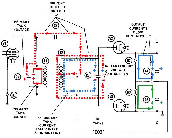
Fig. 7-8. Operation of the tuned discriminator at the center frequency
third quarter-cycle.
The fact that the two resultant voltage waveforms of Fig. 7-10 are exactly 90°, or a quarter of a cycle, apart stems directly from the original assumption that the oscillating tank voltage (shown in dotted blue) and the capacitively coupled voltage (shown in dotted red) are equal in amplitude. Otherwise, the phase of the resultant voltages would be shifted. As a result, both peaks of positive voltage (waveforms D and E of Fig. 7-10) would shift in phase and occur closer in time to the positive peak voltage of the larger driving voltage.
As an extreme example, imagine the inductive coupling be tween coils L1 and L2 were reduced until the oscillation of electrons in the secondary tank ( the current shown in dotted blue) could barely be sustained and almost vanished. The amplitude of waveforms Band C of Fig. 7-10 would progressively diminish, too. Should oscillation cease, these two waveforms would be straight horizontal lines coinciding with the reference line. The sum voltage waveform A and each line would give a waveform equal in size and phase to voltage waveform A. Obviously, then, the two diodes would conduct at the same instant. This would occur at the end of the first quarter-cycle, when the primary tank voltage (represented by waveform A) had reached its positive peak.
As another extreme example, consider what would happen if the voltage coupled from the primary to the secondary tank via capacitor C2 were reduced almost to the vanishing point. Voltage waveform A would decrease in amplitude and, if no voltage were coupled across C2, would become a straight line coinciding with the reference line. Obviously, if this hypothetical waveform A were added to C, the resultant waveform would be in phase with C and also have the same amplitude. The upper diode would then have maximum conduction at the end of the second quarter-cycle.
By the same token, the algebraic sum of waveform B and a waveform of zero amplitude (a straight line) will give a wave form which is in phase with waveform Band has the same size.
The lower diode will thus have its maximum conduction at the end of the fourth quarter-cycle.
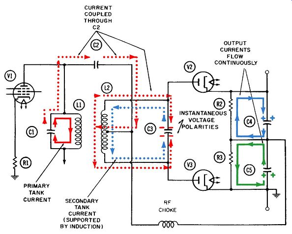
Fig. 7-9. Operation of the tuned discriminator at the center frequency
fourth quarter-cycle.
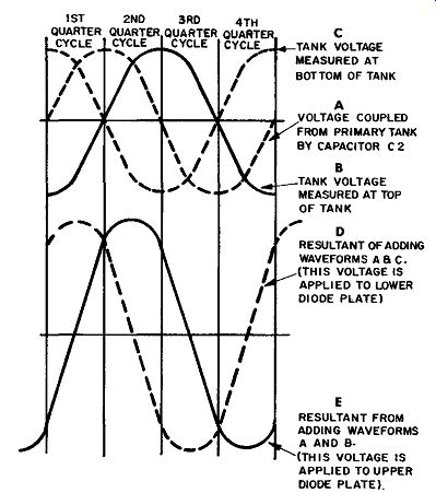
Fig. 7-10. Waveforms in the tuned discriminator circuit when operated
at the resonant frequency.
Operation Above the Center Frequency:
Figs. 7-11 and 7-12 show two successive half-cycles in the operation of the tuned discriminator. Here the operating frequency is higher than the center frequency. From Fig. 7-1 we see that the carrier frequency is modulated by the audio voltage, so that frequencies higher than the center frequency represent positive peaks of audio voltage and lower frequencies represent negative troughs.
The voltage polarities applied to the two diode plates are indicated by red and blue plus and minus signs on both plates of tank capacitor C3. The blue signs represent the voltage polarity resulting from the oscillating tank current. Observe that during the first half-cycle of Fig. 7-11, this voltage makes the upper plate of C3 positive and the lower plate negative. But something else occurs during this same half-cycle-both plates are made negative by virtue of being coupled capacitively to the voltage at the top of the primary tank. The coupling current, shown in dotted red lines, alternately delivers electrons to both sides of the secondary tank during the first half-cycle, making both sides of the tank negative. During the second half-cycle, it then withdraws electrons and both sides are made positive.
As a result of these two voltages acting independently on the secondary tank circuit, neither diode can conduct electrons during the first half-cycle. The reason is that the lower-diode plate is at a high negative voltage, while the upper-diode plate remains at a neutral voltage. (In essence, the positive and negative components cancel each other at the upper-diode plate.) The lower diode conducts electrons during the second half-cycle because both applied voltages are positive. The upper-diode plate is again at a neutral voltage, and the positive and negative applied voltages cancel each other as before. Thus we have a means of assuring that the lower diode will conduct more electrons than the upper diode when the circuit is operated above the center frequency. This fact has a direct bearing on the voltages developed across output resistors R2 and R3-and on the sum of these two voltages, which is the discriminator output voltage.
Under the conditions shown in Figs. 7-11 and 7-12 (the upper diode not conducting), no current will flow through resistor R2 and no voltage will be developed across it. Consequently, the total output voltage across both resistors will equal the voltage drop across R3 resulting from the lower diode current flowing through it. Therefore the output voltage, measured at the top of the resistor combination, will be negative.
The results indicated by this discussion would appear to conflict with the classical response curve of an FM detector in Fig. 7-5. As shown, the voltage is positive above the center frequency and negative below it. This discrepancy is not of great significance. It stems from the assumptions made at the outset, and in particular from the manner in which these assumptions were de fined and interpreted. It is accepted, for instance, that when two tank circuits are inductively coupled together and operated at resonance, their oscillatory voltages will be a quarter of a cycle out of phase with each other. However, it was an act of interpretation to assume that the points for measuring and comparing these two voltages would be the tops of the two tank circuits, as they are drawn in the various circuit diagrams in this section, beginning with Fig. 7-6.
Depending on the manner in which a particular transformer is wound or is connected into the circuit, we might just as naturally be comparing the voltage at the bottom of the secondary tank with the voltage at the top of the primary. If this were done, the output voltage of this tuned discriminator would then be consistent with the classical response curve of Fig. 7-5.
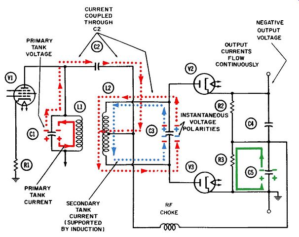
Fig. 7-11. Operation of the tuned discriminator above the center frequency--first
half-cycle.
Actually, the human ear cannot differentiate between the negative and positive half-cycles, so it makes no difference whether they are reproduced in accordance with the original modulating signal or not. Also, each stage of amplification following the detector will shift the phase of the signal 180°. Therefore, if it is desired to have the same polarity as the original modulating signal at the output, all that is required is to use an odd number of amplifying stages following the detector.
Simplifying Assumptions The example in Figs. 7-11 and 7-12 is a special case in which two assumptions have been made to simplify the discussion. These assumptions are that (1) the two voltages applied to the diodes are equal in amplitude or strength, and (2) although exactly in phase on one side of the secondary tank, the two voltages are exactly out of phase on the other side. Fig. 7-13 shows this phase relationship.
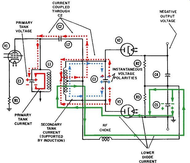
Fig. 7-12. Operation of the tuned discriminator above the center frequency--second
half-cycle.
Waveform C represents the amplitude of the oscillatory tank voltage at the lower side of the tank, and waveform A, the amplitude of the voltage coupled to the tank by capacitor C2. These two waveforms are essentially equal in amplitude and phase, and their algebraic sum is the waveform shown at E. (Note. that it has twice the amplitude of either applied voltage.) This voltage is applied to the plate of lower diode V3 during the second half-cycle. As a result, the plate is made positive and is able to conduct electrons.
Waveform B of Fig. 7-13 represents the amplitude at any instant when the oscillatory tank voltage is measured at the upper side of the tank. This waveform is assumed to be essentially equal in amplitude to voltage waveform A but 180° (half a cycle) out of phase with it. The algebraic sum of these two waveforms is a sine wave of extremely low amplitude ( waveform E) . If the two applied voltages were exactly equal in amplitude, waveform E would have zero amplitude and thus be a straight line. This sine wave of voltage is applied to the upper-diode plate and prevents this plate from becoming sufficiently positive that the tube will conduct.
There is only one occasion when two inductively coupled tuned circuits like these will have two tank voltages with the precise phase relationship shown. This is when the two coils are slightly overcoupled and when the operating frequency has one particular value which is somewhat higher than the true resonant frequency to which the circuits are tuned. What this operating frequency is depends both on the degree of coupling between coils and on the respective circuit Q's.
The response curve for overcoupled circuits indicates that new resonant peaks occur at two particular frequencies, one above resonance and one below. It is precisely at these two new frequencies that the two tank voltages are either 180° out of phase, or exactly in phase, with each other.
Figs. 7-11, 7-12, and 7-13 apply to operation at the one and only frequency above resonance at which the two tank voltages are exactly 180° out of phase.
In these examples, the terms "in phase" and "out of phase" mean the phase relationships of the two tank voltages are being compared as measured at the tops of the two tanks. In considering the phase of a tank voltage-particularly at each end of a tank it is always desirable to clarify which voltage is under discussion, since the ones at the top and bottom of any oscillating tank arc themselves 180° out of phase with each other.
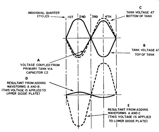
Fig. 7-13. Waveforms in the tuned discriminator circuit when operated
above the center frequency.
Operation Below the Center Frequency:
Fig. 7-14. Operation of the tuned discriminator below the center frequency--first
half-cycle.
Figs. 7-14 and 7-15 show two successive half-cycles in the operation of the tuned discriminator, when the operating frequency is below the center frequency. The same simplifying assumptions have been made as in the previous example. The two tank voltages are now assumed to be exactly in phase, with their positive voltage peaks (measured at the tops of the tanks) occurring at the same instant. This is portrayed in Fig. 7-16, where voltage waveforms A and B are in phase with each other and have essentially the same amplitude. Their algebraic sum is shown by waveform D, which reaches its positive peak during the middle of the first half-cycle. This is the moment when the most electrons are conducted through upper diode V2. Fig. 7-14 shows this tube current in solid blue. It follows the expected path from cathode to plate within the tube, then downward through the upper half of winding L2 to the center tap. Here it exits from the coil and returns, via the external line, to the junction of output resistors R2 and R3. This upward flow signifies that the voltage is more positive at the top of R2 than at the bottom.
This positive voltage (indicated in Fig. 7-14 by the blue plus sign on the upper plate of capacitor C3) is preserved throughout the half-cycle of Fig. 7-15, when diode V2 has a negative plate voltage and does not conduct electrons. Fig. 7-15 shows this positive capacitor voltage continuing to draw electron current upward through resistor R2 in an attempt to discharge itself to zero volts.
Waveform C of Fig. 7-16 represents the oscillatory tank voltage as measured at the bottom of the secondary tank circuit. Since it is exactly out of phase with waveform A and essentially of equal amplitude, the algebraic sum of the two is of very low amplitude, as shown by waveform E. In the hypothetical example where the two applied voltages have the same amplitude, their resultant will be a straight line coinciding with the reference line.
Since waveform D achieves no significant amplitude, the plate of diode V3 has a very low positive voltage applied to it during the second half-cycle. Hence, no appreciable current flows through it during the entire cycle. Thus, the output voltage of the discriminator is made up entirely of the negative voltage developed across resistor R2 by virtue of the electron current flowing through upper diode V2.
The examples used here--where upper diode V2 does not con duct when operating above the center frequency, and the lower diode does not conduct when operating below the center frequency-are extreme cases which might not be desirable or even realized in practice. Nevertheless, the output voltage achieved across the two output resistors, when the upper diode does not conduct, would clearly be the maximum attainable negative voltage. Likewise, the output voltage achieved when the lower diode does not conduct would clearly be the maximum attainable positive voltage. The resultant audio voltage, as the output varies be tween these two positive and negative peaks, would have the maximum amplitude attainable and would correspond to the waveform in Fig. 7-1C.
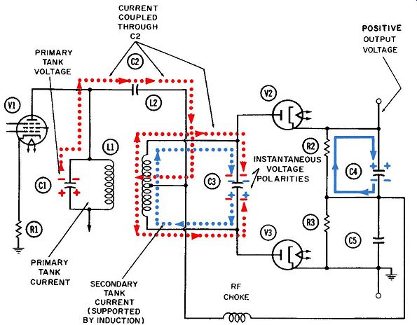
Fig. 7-15. Operation of the tuned discriminator below the center frequency--second
half-cycle.
Audio voltages of lower amplitude, corresponding to the wave form of Fig. 7-1A, would be achieved with smaller deviations of the carrier from the center frequency. In all such cases, the operating conditions shown in Figs. 7-11, 7-12, 7-14, and 7-15 would be modified. The 180 phase relationships between the two applied voltages would of course not exist, and each diode would conduct some electrons above and below the center frequency.
Referring to Fig. 7-10, note that the phase relationships be tween the two applied voltages represent the normal condition when no modulation exists. Consequently the carrier does not deviate from the center frequency. When two tuned tank circuits are inductively coupled and are operating exactly at resonance, their tank voltages will be 90° out of phase with each other.
When applied to the carrier frequency at the transmitter, an audio voltage of small amplitude causes the carrier frequency to deviate slightly in both directions. At the positive audio peak it goes above the center frequency, and at the negative audio trough it goes below. Any variation from this resonant, or center, frequency destroys the precise 90 ° phase relationship between the two tank voltages. Inevitably, voltage waveform A is moved closer to waveform C (when above the center frequency) and farther from waveform B. Under these conditions waveform D would increase slightly in amplitude, causing a slightly greater current flow through the lower diode than existed at the center frequency. At the same time, waveform E would decrease slightly in amplitude, and fewer electrons would flow through the upper diode. At this instant, the output voltage has a small negative value.
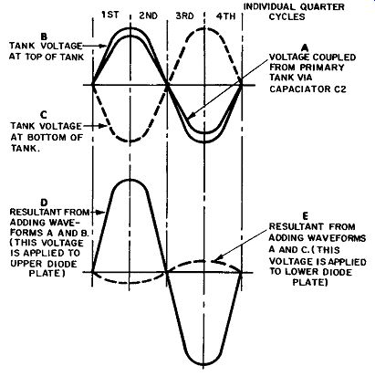
Fig. 7-16. Waveforms in the tuned discriminator circuit when operated
below the resonant frequency.
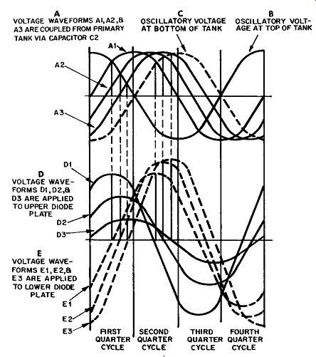
Fig. 7-17. How variations in phase between the two driving voltages will
increase the voltage applied to the lower diode and decrease the voltage
applied to the upper diode when operating above the resonant, or center,
frequency.
When the carrier deviated slightly below the center frequency, an opposite set of conditions prevails. Waveforms A and B move closer together in phase. The amplitude of their resultant (wave form E) increases slightly and a few more electrons flow through upper diode V2. Waveforms A and C move farther apart in phase. Their resultant (waveform D) decreases slightly in amplitude, and not as many electrons flow through lower diode V3. At this instant, the detector output voltage will have a small positive value.
For greater frequency deviations, the detector output voltage will increase. Since it goes from positive to negative whenever the carrier frequency goes from below to above resonance, the frequency of the modulating audio voltage as well as its amplitude will be accurately reproduced.
The key to the operation of this type of circuit is to understand the phase relationships between two tuned radio-frequency circuits which are inductively coupled together and are operated near their resonant frequency. The significant fact is that under these conditions the tank voltages of two circuits will be exactly one-quarter cycle out of phase at resonance. As the frequency increases above resonance, this phase difference will increase to a maximum of half a cycle, or 180". Conversely, as the frequency decreases below resonance, this phase difference will decrease from 90° toward zero, meaning the two tank voltages are exactly in phase.
The phase relationships between these two oscillatory tank voltages are important in this circuit only because of what happens when the two voltage waveforms are added algebraically. The use of both capacitive and inductive coupling provides the means for adding these two voltages. Fig. 7-17 shows several sample wave forms resulting when the carrier frequency deviates farther and farther above the resonant, or center, frequency. It can be seen from this figure that the amplitudes of the waveforms at D increase as the frequency excursion does, whereas the amplitude of the waveforms at E decrease in like amounts.
The waveform, shown as curve A1 in Fig. 7-17 and corresponding to waveform A of Fig. 7-10, reaches its positive peak a quarter of a cycle after waveform B (the latter is the oscillatory voltage measured at the top of the tank), and a quarter of a cycle before waveform C (the oscillatory voltage measured at the bottom of the tank). These phase relationships exist only at the resonant, or center, frequency.
Curve A2 shows how the phase of the capacitively-coupled voltage waveform has shifted slightly to the right as the frequency deviates above resonance. This reduces the phase difference be tween waveforms A2 and C and increases the amplitude of their resultant (the curve labeled E2). This phase shift of waveform A2 also increases the phase difference between it and waveform B, and thus decreases the amplitude of their resultant (the curve labeled D2) .
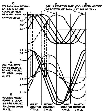
Fig. 7-18. How variations in phase between the two driving voltages will
increase the voltage applied to the upper diode and decrease the voltage
applied to the lower diode when operating below the resonant, or center,
frequency.
Waveform A3 represents a further deviation in phase of the primary tank voltage when compared with the phase of the secondary tank voltage. Waveform A3 moves closer to coincidence with waveform C. As a result, their sum-shown as curve E3 undergoes another increase in amplitude. Curve A3 also moves farther away from coincidence with waveform B, so that the amplitude of their resultant (labeled curve D3) again decreases.
A similar set of waveforms has been drawn in Fig. 7-18 to illustrate the phase relationships between the two applied voltages when operating below resonance, and the changes in amplitude of the resultant voltages applied to the two diode-detector plates.
With such a set of curves, waveform A shifts to the left instead of the right, bringing it toward phase coincidence with waveform B and toward phase opposition with waveform C. Under these conditions, waveform D progressively increases in amplitude as the frequency excursion does, while waveform E progressively de creases in amplitude.
In Fig. 7-18, waveforms A1, B, and Care identical to the wave forms having the same designations in Fig. 7-17. Waveforms A4 and A5, however, represent the progressive shifts in phase of the directly-coupled voltage with respect to the phase of the secondary tank voltage.
Inspection of Fig. 7-18 should reveal that the various waveforms are related as follows: Al plus C combine to produce waveform E1.
A4 plus C combine to produce waveform E4.
AS plus C combine to produce waveform ES. Al plus B combine to produce waveform D1.
A4 plus B combine to produce waveform D4.
AS plus B combine to produce waveform D5. Waveforms D and E represent the total voltages applied to the plates of the upper and lower diode-detector tubes, respectively.
Consequently, their amplitudes will be roughly proportionate to the amount of electron current through each diode, and therefore to the voltages developed across R2 and R3 during any RF cycle.
Because of the opposing polarities of the voltages developed across R2 and R3, the total output voltage across the two resistors will always be negative when operating above resonance and positive when operating below.