AMAZON multi-meters discounts AMAZON oscilloscope discounts
(<< cont. from part 1)
5. TIN-LEAD PLATING SOLUTION
After the plating tank has been properly leached, the preparation of the plating solution may begin. For our purposes, a high-throwing power formulation will be used to electrodeposit 60/40 tin—lead alloy onto the copper conductor pat tern surface. The solution described is a high-acid, low-metal (tin and lead) mix ture formulated under the trade name HI-THRO, manufactured by the Allied Chemical Corporation in Morristown, N.J., under U.S. Patent 3,554,878. The plating bath is made up of the following chemicals and compounds:
1. Stannous fluoborate concentrate, 51.0% by weight
2. Lead fluoborate concentrate, 51.0% by weight
3. Fluoboric acid, 49% by weight
4. Boric acid
5. Stabilized liquid peptone solution (available from Allied Chemical Corporation)
6. Water
Stannous and lead fluoborate are used to provide the source of metal in the plating bath. Because variations in the metal content of the plating bath will adversely affect the content of the alloy deposited, both the stannous and lead fluoborate additives must be carefully controlled when preparing the bath so that it will contain 60% by weight of tin as a metal and 40% by weight of lead as a metal.
The fluoboric acid aids in increasing the conductivity of the bath and improves the grain quality of the deposit by making it finer and smoother. Pep- tone also improves the fine-grained deposit and inhibits the formation of “trees,” which are small growths of deposit extending away from the conductor pattern. Boric acid aids in maintaining stability by minimizing the decomposition of the fluoborates in solution.
The chemicals and compounds necessary to prepare a 10-gallon bath of HI-THRO tin-lead fluoborate plating solution are listed in TABLE 5. The table includes the required amounts and the order of mixing the ingredients.
For purposes of preparing a plating bath for the 6-gallon tank previously discussed, TABLE 6 lists the amount of each ingredient and the order of mix ture. The required amount of each of the ingredients was derived by taking (0.6) of the amounts listed in TABLE 5.
The 6-gallon plating solution is prepared by first placing one-half of the required amount of water (0.96 gallon or 3633 milliliters) into the plating tank.

TABLE 5 Formulation of 10 Gallons of Tin—Lead Plating Solution

TABLE 6 Formulation of 6 Gallons of Tin—Lead Plating Solution
To 1500 milliliters of hot water, 1.11 pounds (503.5 grams) of boric acid is added and stirred until it is completely dissolved. This solution is then added to the plating tank and stirred. The following are then stirred into the plating tank in the order given: 0.126 gallon (480 milliliters) of lead fluoborate solution; 3.6 gal- ions (13.62 liters) of fluoboric acid; 0.27 gallon (1020 milliliters) of stannous fluoborate solution; and 0.102 gallon (390 milliliters) of stabilized peptone. The remaining water (2137 milliliters) is added to the tank to complete the bath solution. The solution is thoroughly stirred and allowed to settle overnight before use.
The height of the solution in the tank should be marked on the outside to note any decrease due to evaporation. Any significant decrease of solution should be replaced so as to return it to the original level in the tank. The bath should be maintained at room temperature and loosely covered with sheet plastic when not in use to protect the solution from dust and other foreign matter.
All plating solutions require periodic chemical analysis. In alloy plating, the ratio of metals deposited must be maintained within narrow limits. The techniques of chemical analysis for the type of bath just described are beyond the scope of this book. However, since the amount of solution described in TABLE 6 is relatively small and not significantly expensive, the entire bath should be replaced if plating problems are encountered. A fresh batch of solution can be used successfully for a reasonable length of time if extreme care is exercised to minimize the introduction of organic contaminations into the solution. Detailed chemical analysis techniques may be obtained from Allied Chemical Corporation for HI-THRO plating solution.
6. 60/40 TIN-LEAD PATTERN PLATING
After the board has been copper pattern plated, rinsed, and dipped into the 10% fluoboric acid solution, it is ready for the solder plating process. The power supply is first turned on and set to a low reading ( ampere) to activate the plating solution. The racked board is then removed from the fluoboric acid bath and placed into the solder plating tank. The rack is secured onto the cathode work rod with the thumb screw and the power supply is adjusted to the correct current density. The current setting determines the proper alloy plating and needs to be properly set. The manufacturer recommends that the optimum current density be 20 amperes per square foot ( 140 mA/in. for this plating solution. In Sec. 1 it was calculated that the conductor patterns and thief areas on both sides of the preamplifier board each have a surface area of 10 square inches. Therefore, the plating power supply must be set as follows:
current = current density x total surface area
= 140 milliamperes / square inch x 20 square inches
= 2800 milliamperes = 2.8 amperes

FIG. 7 Properly processed PTH board through copper and solder electroplating.
It will be noted that when the power supply is set at 2.8 amperes, the output voltage is low (in the order of 1 volt or less) for this plating solution.
The thickness of the plating onto the pc board is a function of the current density and the plating time. For the HI-THRO alloy bath, 60/40 tin-lead is plated at a rate of 0.0001 inch (0.1 mil) every 2.3 minutes. To achieve a plating thickness of 0.3 mu requires 6.9 minutes, and 0.5 mil requires 11.5 minutes of plating. A minimum of 0.3 mil of plating thickness is required for the tin—lead alloy to provide an effective etching resist. A plating time of 7 minutes has been established as optimum to provide the pc board with the minimum required plating thickness.
After the pc board has been plated, the power supply is turned down to a few milliamperes to keep the tank “live,” the motor driving the cathode rod is turned off, and the rack is removed from the cathode work rod. Finally, the power supply is turned off. The board is then thoroughly rinsed in cold tap water for at least 1 minute and then dried. Inspection of the plating should re veal a smooth, fine-grained deposit with a light dull-gray surface having no apparent dark streaks. A properly plated pc board is shown in FIG. 7.
7. RESIST STRIPPING
The Laminar AX resist previously applied to the pc board may now be removed by chemical stripping since it has served its purpose. The Dynachem Corporation provides an alkaline solution that will remove the resist by simple immersion. For Laminar AX resist, 400K stripper is available as a concentrate. The stripping solution is prepared by mixing 1 part of 400K stripper to 9 parts of water in a beaker. The stripping solution is then heated on a hot plate to 130°F (54 °C). The temperature should be checked with a laboratory thermometer. Immersion of the pc board into the stripper for approximately 2 minutes will dissolve the resist in the hot water. The board is then removed from the stripper and rinsed first in hot tap water and then in cold tap water for at least 1 minute to completely remove any remaining film residue. It is recommended that the board surface be gently scrubbed with a nylon bristle brush while under the hot-water rinse. Since the stripper solution is highly alkaline, chemical-resistant gloves should be worn.
8. ETCHING
After stripping the resist from the processed pc board, it is ready to be etched. The copper conductor pattern is protected with a 0.3-mil-thick layer of 60/40 tin-lead alloy while the exposed surrounding areas are unprotected and can be removed by etching. Etching is accomplished in a similar manner, as described in Section 13. However, ferric chloride, which was used in Section 13 as the etching solution, cannot be used, as it will attack the tin—lead alloy as well as the exposed copper. The tin—lead alloy plating acts as the etch “resist” and an etchant solution must be used that will be effective in attacking the exposed copper without adversely affecting the plating. Four common etching solutions can be used for this purpose: alkaline ammonia, chromic-sulfuric acid, peroxide/sulfuric or modified ammonium persulfate. Both the alkaline ammonia and the chromic-sulfuric acid solutions produce noxious and poisonous fumes, especially when heated. Peroxide/sulfuric solution requires constant monitoring and control. When using these solutions as etchants, extreme caution and good ventilation are required. For these reasons, alkaline ammonia, chromic-sulfuric acid, and peroxide/sulfuric are limited to industrial applications. The modified ammonium persulfate solution is much safer to use and is the best choice for prototype applications. This etchant solution is made by dissolving 2 pounds (0.91 kilogram) of ammonium persulfate crystals per gallon (3.785 liters) of de ionized water at a temperature of 120°F (49°C). Phosphoric acid is then added in the amount of approximately 50 milliliters per gallon of etching solution. The formulation of 10 gallons of modified ammonium persulfate etchant is shown in TABLE 7.
Etching double-sided pc boards is best accomplished with the use of a spray etcher, such as that shown in FIG. 8. This etcher allows for both sides of the pc board to be etched at the same time. The spray etcher is operated at a temperature of 110 to 120°F (43 to 49°C). The time required to accomplish the etching is a function of the temperature and the amount of copper in the solution. A 1-ounce copper board should satisfactorily be etched in 3 to 5 minutes. As more boards are etched, additional copper goes into the solution and a point will be reached where etching time will exceed 6 minutes. At this point, the etchant should be replaced with fresh solution. Where small volumes are involved, it is advisable to prepare a fresh batch daily.
After the board has been etched, it is rinsed in cold tap water and thoroughly dried with paper towels. The etched pc board is shown in FIG. 9.
TABLE 7 Formulation of 10 Gallons of Ammonium Persulfate Etchant
FIG. 8 Spray etcher for both single- and double-sided pc boards.
FIG. 9 A pc board after etching.
9. SOLDER FUSION
After the pc board has been etched, it is now ready for final processing: drilling, shearing, component assembly, and component soldering. However, an interim step is recommended at this stage of processing. This process is called fusion, sometimes referred to as reflow, and involves heating the 60/40 tin—lead alloy electroplated onto the copper surface to a temperature sufficient to melt the plating and fuse it to the underlying copper. The following advantages are realized through this process: (1) improved solderability, (2) extended shelf life, (3) elimination of solder overhang which may have resulted after the etching process, (4) a check to observe if dc-wetting of the copper surface is a problem, and (5) a rough check on the metal ratio of plating. Items 1, 2, and 3 are self-explanatory. Items 4 and 5 will be discussed in detail. During the pattern-plating process, the 60/40 tin—lead metals have been plated onto the copper surface. The plating has not been alloyed with the copper but is adhered through a metallic bond. For alloying to occur, the solder must be elevated to its melting temperature.
If the solder has been plated to a clean copper surface, the fused solder will appear as bright and shiny over the entire conductor path areas. After fusion, an indication of an improper bond is a nonuniform surface showing nodules of solder. This dc-wetting condition is a probable indication of an unclean copper surface and the board should be rejected to avoid further problems during the component soldering process, whether it be by hand, dip, or wave methods. The fusion process, then, is a quality-control check on the cleaning process. If de-wetting occurs after fusion, the cleaning process needs to be improved and/or corrected.
Fusion can also be used as a means of roughly checking the tin-lead ratio being plated. Reference to the tin—lead fusion diagram in Fig. 15.1 shows that at temperatures between 361 and 400°F, the range of tin-lead solder alloys that will melt are 55/45 through 60/40 to 80/20. If the plating has not melted and formed an alloy with copper after the fusion process, this is an indication that the metal content of the plating bath is out of balance and should be re placed.
Fusion is accomplished in an infrared drawer-type oven, similar to the one shown in FIG. 10. This style of oven consists of a wire belt drawer with infrared heating elements positioned above and below, a preheat timer, a high- intensity timer, a cycle button, and an exhaust blower system. The recommended time settings for 1/16-inch pc board stock are 15 seconds for the preheat timer and 9 seconds for the high-intensity timer.
Before the pc board is placed into the oven drawer, it must be fluxed with a solder-fusing liquid. This liquid is applied to all areas of the pc board by hand brushing, spraying, or roller coating. The fusing liquid should be a mildly acidic flux that is completely water soluble. One such flux is Solder Flow No. 211 1A available from Gb-Quartz Ovens, Inc.
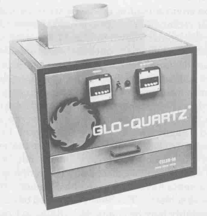
FIG. 10 Bench-type solder fusion oven. Courtesy of Glo-Quartz Ovens,
Inc.
The purpose of the flux is to prevent air from contacting the molten solder, to minimize the formation of oxides, to hold any impurities in suspension so that they will not interfere with the alloying process, and to reduce the possibility of de-wetting.
After the pc board has been properly fluxed, it is inserted into the drawer of the oven. The oven door is closed and with the two timers set, the cycle but ton is activated. During the preheat cycle ( 15 seconds) the board is elevated to a temperature of approximately 200°F (93 °C) to reduce the possibility of thermal shock. At the end of the preheat cycle, the high-intensity cycle ( 9 seconds) automatically increases the board’s temperature to approximately 400°F (204°C), melting the plate alloy and fusing it to the copper surface. The board is allowed to cool for a few minutes before removing it from the oven. The result of fusion is a conductor pattern having a bright and shiny appearance.
Because Solder Flow No. 211 1A is a mildly acidic solution, the residue remaining on the copper surfaces must be completely removed. This is best accomplished by briskly brushing both sides of the pc board in warm water using a nylon bristle brush. A final rinse under a cold-water tap for 30 seconds on each side followed by paper-towel drying completes this phase of the pc board processing.
10. FINAL FABRICATION PROCESSES
The final sequence of operations required to complete the pc board is (1) cutting the panel to size (or routing to shape), (2) assembling the components and hard ware, and (3) soldering. Since most of these operations have been discussed in earlier Sections as they pertain to single-sided pc boards they will be briefly mentioned here only as they relate to double-sided boards.
For prototype work, shearing the pc board to the inside edges of the corner brackets is usually satisfactory. Shears such as those in Section 4 are suit able for this purpose. Shearing leaves the edges of the board rather rough. These rough edges are easily smoothed by placing a fine file onto a workbench and pushing the board edges across the file. About six passes across the file for each edge are sufficient. If a smoother finish than can be obtained by the file alone is required, the edges can be firmly rubbed with No. 320- or 400-grit abrasive paper. When the edge color matches that of the board surface, optimum smoothness is achieved.
In a production environment or if boards are to be shaped or profiled into other than square or rectangular shapes, a routing operation is required. For this purpose, the driller/router shown in FIG. 2 is used. Panels to be routed are first pinned together and secured onto the worktable. Multifaceted carbide router bits, which are designed for cutting along their sides, are used for routing. The panels are cut to finished size and shape as dictated by the programmed instructions in the machine’s computer memory.
After the board has been sheared or routed, hardware requiring staking or swaging should be installed before any components are assembled onto the board. (Staking and swaging are discussed in Section 14.) Similar to single- sided boards, components that are not sealed or have materials that can be adversely affected by flux-cleaning solvents should not be initially installed. (Refer to Section 14 for a detailed discussion on component assembly.) After all noncritical components have been assembled on one side, the opposite side is coated with flux and soldered. The board is cleaned of all flux residue and the final component assembly may be completed. (Refer to Section 15 for detailed discussions on proper soldering procedures.)
FIG. 11 Completely processed and assembled preamplifier pc board.
Because electrical interconnections between terminal pads on opposite sides of the board are made with the plated-hole barrels, applying solder to component leads on the circuit side is all that is required to complete the board. Solder fillets will automatically form about the leads entering from the terminal pads on the component side by wicking action through the plated holes. The completely assembled and properly soldered double-sided preamplifier board is shown in FIG. 11.
EXERCISES
A. Questions
1 What are the three methods used to determine the image area of a pc board?
2 Calculate the thief area of a 6- by 9-inch board that has a 4- by 7-inch image area.
3 Solve for the image area, in square inches, for one side of a double-sided board design having 15 resistors with 0.125-inch pads, 20 sixteen-pin DIP ICs, 5 eight-pin round ICs, and 85 inches of 0.040-inch conductors. Use TABLE 1 as a guide.
4 Using the values obtained in Problems 19.2 and 19.3, find the total area to be plated for (a) one side and (b) both sides of the pc board.
5 Determine the total area of 1 ounce per square foot copper to be pattern plated (double-sided board) if W is 185.63 grams and W is 179.21 grams.
6 Calculate the proper current settings to pattern plate copper onto a double-sided board having a total area of (a) 121 square inches and (b) 3.6 square feet.
7 With reference to TABLE 4, which is based on an ideal of 100% cathode efficiency, calculate the practical time to plate 1.5 mils of copper with a current density of 30 amperes per square foot.
8 Using the values obtained in Problems 19.4 and 19.5, calculate the correct power supply setting for solder plating.
9 How much does each of the plating processes (copper pattern plating and solder plating) add to the thickness of the metal surfaces?
10 What reduction in hole diameter size results from pattern and solder plating?
11 What are the recommended current densities for electroplating copper? For electroplating solder?
12 Briefly describe the difference between flash plating and pattern plating.
13 After the pattern plating and solder plating have been completed, how is the resist film removed from the pc board?
14 Define the term solder fusion. By what other name is this process known?
15 What are the advantages to the use of the solder fusion process?
B. True or False
Choose T if the statement is true, or F if any part of the statement is false.
1 In the pattern plating process, the dry-film photo-resist acts as a plating stop-off and the pattern-plated solder acts as an etchant stop-off. T F
2 The solder reflow process causes the solder to alloy with the underlying copper conductor pattern. T F
3 The thief area of a 6-by 9-inch pc board having a 1-inch-wide border is 29 square inches. T F
4 The optimum current density for plating solder is 30 amperes per square foot. T F
5 To provide an effective etching resist, a minimum thickness of plated solder is 0.003 inch. T F
6 For the plating of tin—lead alloy, an anode-to-cathode surface area ratio of approximately 3:1 is recommended. T F
7 The anode and cathode work rods in a plating tank are made from solid copper rod stock. T F
8 The most accurate method of determining the image area to be pattern plated is the calculation method. T F
9 The optimum thickness of pattern-plated copper is 3 mils. T F
10 Ferric chloride cannot be used to etch solder-plated pc boards. T F
C. Multiple Choice
Choose the correct answer for each statement.
1 The three methods used to determine pattern area are calculation, using automatic equipment and (weight gain, weight loss).
2 It takes approximately (60 seconds, 60 minutes) to pattern plate 1 mil of copper.
3 To produce an effective etch-resist, a minimum of (0.3 mils, 30 μ-inches) of solder is required.
4 For pattern plating, the pc board is securely attached to the (anode, cathode) rod of the plating tank.
5 The time required to pattern plate 60/40 tin—lead to the minimum required thickness is approximately (7 seconds, 7 minutes).
6 Dynachem 400K solution should be (heated; cooled) prior to resist strip ping.
7 Etching a pattern plated pc board should be accomplished with a solution of (ammonium persulfate, ferric chloride).
8 A de-wetting condition exhibited by pc boards after the reflow process is the result of a (good; poor) copper surface cleaning cycle.
D. Matching Columns
Match each item in column A to the most appropriate item in column B.
COLUMN A | COLUMN B
1. Ammonium persulfate 2. Peroxide/sulfuric 3. Copper pattern plating 4. Solder pattern plating 5. 400K 6. LAC-41 7. Reflow |
a. Stripper b. 30 A/ft.^2 c. Fusion d. Cleaner e. Etchant f. Micro-etch g. 20 A/ft.^2 |