AMAZON multi-meters discounts AMAZON oscilloscope discounts
LEARNING OBJECTIVES:
Upon completion of this Section on the final fabrication processes for double-sided pc boards, the student should be able to:
1. Determine the copper image area of a conductor pattern.
2. Set up a cleaning line to prepare pc boards for copper pattern plating.
3. Plate copper onto the conductor pattern of pc boards.
4. Prepare a tank and accessories for tin—lead pattern plating.
5. Prepare tin—lead plating solution.
6. Solder-plate the conductor pattern of pc boards.
7. Prepare resist stripping solution and remove the resist from pc boards.
8. Prepare a modified ammonium persulfate solution to use with a spray etcher to etch pc boards.
9. Use an oven to reflow solder on pc boards.
10. Shear or route pc boards to final size and shape.
11. Mount all hardware and components onto pc boards.
12. Properly flux and solder components to pc boards.
0. INTRODUCTION
In Section 18, 1: 1 diazo phototools were used to image the laminated pc board, which had previously been completely covered with a 125-pinch layer of copper (Section 17), to form the conductor path and terminal pad patterns. The result of this imaging is shown as the first sequential step in the processing flow chart of FIG. 1.

FIG. 1 Basic flow chart with pictorial sequence of the pattern plating
process, including etching and reflow.
The next phase of fabrication is the pattern-plating process. This involves plating of the imaged pattern with additional copper followed by a layer of tin lead alloy (solder). The pattern-plating process first adds on an additional thickness of approximately 0.001 inch (1 mil) of copper onto all the exposed conductor pattern as well as the inside surfaces (barrels) of all the drilled holes. This will ensure continuous metal paths having good electrical integrity of all through-hole connections from one side to the other. The solder (60/40 tin—lead alloy) is then electroplated over the conductor pattern and the hole barrels to a thickness of approximately 0.0003 inch (0.3 mil). The solder serves a dual purpose: first as an etchant resist and subsequently as a fused protective coating against oxidation for the entire pattern. This solder coating improves board shelf life and promotes improved soldering to the pattern. Refer again to FIG. 1 to see the results of pattern plating.
After the image has been pattern plated, the dry-film photo-resist, which is used as a plating stop-off (plating resist to all areas of unimaged copper) during the plating process, has now served its purpose. It may now be chemically stripped (removed) from the board, thereby exposing the underlying layer of copper, which was flash plated onto the board’s foil. (See the next sequential step in FIG. 1.) This is the copper which was not pattern plated and thus is exposed to the etchant which will remove it completely from the board. The copper image, which is protected by the pattern-plated solder (now serving as an etchant stop-off), will not be attacked by the etchant and will thus remain on the board. Note in FIG. 1 that all conductor paths, terminal pad areas, and all connections made between both sides of the board through plated holes remain after the etching process.
The final process to complete the conductor pattern is called solder reflow. As a result of the stripping and etching process, the solder plating on the conductor pattern image becomes contaminated and must first be chemically treated and then heated to its melting point. This heating process causes the solder to alloy (fuse) with the underlying copper resulting in a much denser and less porous metal that will be less susceptible to oxidation and will enhance the component soldering phase of construction. The processed panels are finally routed (contoured or profiled) to shape to complete their fabrication.
The topics presented in this Section begin with describing several methods of determining the pattern area to be plated for purposes of setting the correct plating current density. Since a detailed discussion on plating copper was presented in Section 17, it will be referred to in this Section only in consideration of copper pattern plating. This is followed by describing the cleaning cycles and a detailed discussion of the solder plating process. Included is a description of etchants which are used with solder as a stop-off. Solder reflow is considered using prototype bench equipment. Finally, board routing is de scribed to profile the panel into a finished double-sided pc board.
1. DETERMINING THE IMAGE AREA TO BE PATTERN PLATED
One of the first steps in preparing to pattern plate is to precisely determine the area of exposed copper to be plated. This is necessary so that the power supply used in the process will be correctly set to result in high-quality plating. There are three methods which can be used to determine the pattern area: (1) the calculation method, (2) the weight loss method, and (3) using automatic area calculator equipment. Each of these methods has its advantages and disadvantages and will be discussed here.
To illustrate each of the methods of determining the image area, we will use the preamplifier component side taping shown in Fig. 16.8. Recall from Sec. 16.7 that the conductor patterns laid out on each side of the board were made as close to equal as possible. Thus, by determining the pattern area on one side, it is assumed that it is the same on the other side.
We will first demonstrate the calculation method. The thief-area calculation presents no special problem, since it is normally a square or rectangular border outside the conductor pattern area. The thief area is calculated as follows ( FIG. 2). The area of the bulk stock is first determined in square inches. The thief area is then obtained by subtracting the available conductor pattern area from the bulk stock area. In equation form, with reference to FIG. 2:
thief area (square inches per side) = (A x B) — (C x D)

FIG. 2 Calculation of thief area. Thief area = (A x B) — (C x D).
(where dimensions A, B, C, and D are in inches). For the preamplifier circuit, the dimensions are
A = 5.0 inches
B = 5.0 inches
C = 4.0 inches
D = 4.0 inches
Therefore,
thief area (square inches per side) = (5 by 5 inches) — (4 by 4 inches)
= (25 square inches) — (16 square inches)
= 9 square inches
The determination of the area of the conductor pattern is not quite as simple. To calculate the copper surface area of the conductor pattern that will face each anode, the area of each of the shaped configurations (i.e., donuts, IC patterns, tape, etc.) used in the layout, reduced to a 1: 1 scale, must first be deter mined. TABLE 1 is provided to aid in this calculation. Many standard patterns used in pc layouts are listed together with their areas in square inches. In addition, several common conductor path widths are given, together with their square inch area per linear inch. The information given in TABLE 1 is for a 1 : 1 scale (i.e., the same size as appears on the pc board). If, for example, a 0.25-inch-diameter donut was used on a 4: 1 layout, the actual 1: 1 scale diameter on the finished pc board would be (0.0625) inch.
The following procedure is used with TABLE 1 to determine the square- inch area of a conductor pattern for one side of a double-sided layout: (1) count the number of donuts of each size used in the layout and multiply their numbers by the appropriate square-inch areas listed for the various terminal pad sizes— this will determine the total area of just the donuts; (2) count and add the total area of each special layout configuration, such as IC patterns; and (3) determine the total length in inches of conductor tape and multiply this length by its area per linear inch. The addition of items 1, 2, and 3 will produce the total conductor area for one side of the pc board. The example shown in TABLE 2 of the fore going procedure for the preamplifier circuit will illustrate its use.

TABLE 1 Areas of Some Standard PC Patterns

TABLE 2 Pattern Area Calculation for Preamplifier Circuit at 1:1 Scale
(One Side)
To calculate the total area to be plated, simply add the previously calculated thief-area to the copper surface area of the conductor pattern. For the component side of the preamplifier layout:
total area to be plated = thief area + conductor pattern area
= (9 square inches) + ( 1.00 square inch)
= 10 square inches
The results of our calculation indicate that there are approximately 10 square inches of conductor pattern area to be plated on each side of the preamplifier board. This value will be used to set the correct power supply setting to obtain the proper plating density.
The apparent advantage to the calculation method is that it requires no special equipment. Even though it yields fairly accurate results, it is extremely time-consuming, especially when dense designs are involved.
The weight loss method of determining pattern area calculation will now be described. This method initially requires that the pc board stock, having 1 ounce per square foot (oz/ft of copper foil on each side, be accurately cut to its initial size to be processed. In the case of the preamplifier board, this is a 5- by 5-inch panel. The panel is next heated at 150°F (65°C) for at least 1 hour to expel any moisture that may be present. It is then precisely weighed to within 0.01 gram on an analytical scale. This initial weight is recorded. It has been found that the panel weight for the preamplifier is 53.724 grams. We will call this weight W. Using the two positives and the imaging techniques discussed in Section 18, the panel is processed through dry-film lamination, exposure, and developing. Since positives are used, the exposed copper image is that of the total conductor pattern and thief areas. Etching the board at this point will remove just those exposed copper areas on both sides of the board. The panel is then rinsed, dried, and again heated to 150°F for 1 hour to remove moisture and then weighed. This new weight measurement is the panel without the copper forming the conductor pattern and thief areas. For our example preamplifier panel, this weight is 49.78 grams. This second weight measurement will be called W. The weight of copper removed from both sides of the board is given by:
W (total pattern) = W — W
= 53.72 — 49.78 = 3.94 grams

FIG. 3 Operator using area calculator. Courtesy of Kahn Instruments,
Inc.
To determine the area in square inches represented by the weight of copper re moved from the board, we simply multiply the total weight loss figure by 5.079. This number represents the area in square inches per gram of 1-ozlft copper. Thus the total pattern area on the preamplifier panel is calculated as follows:
total area (square inches) =5.079 square inches/ gram x 3.94 grams
= 20.0 square inches
Remember that this is the pattern and thief areas on both sides of the board. It can be seen that, as determined by the calculation method, the pattern and thief area of each side is approximately 10 square inches.
The weight loss method is less tedious than the calculation method, but it does require an accurate scale, proper preparation of the sample, and precise measurements to obtain correct results.
The third method of determining the pattern area is with the use of commercial equipment made for this purpose, such as the Kahn Area Calculator, shown in FIG. 3. This instrument is capable of measuring the area of a pat tern on either a positive or a negative phototool to an accuracy of ±2%. Further, the phototool may be either silver halide or diazo film. In using this area calculator, all that is required is that it first be calibrated with the appropriate artwork that comes with the instrument. The Kahn Area Calculator consists of a light-proof box with a fixed-intensity light source in its drawer section. Above this source is a set of light-sensitive resistors (photoconductors) whose resistance is proportional to the intensity of light to which they are exposed. Calibration of the instrument is in units of square inches.
To measure the pattern area using the Kahn Area Calculator, the phototool is first placed in the center of the light table section of the drawer. The entire surrounding area is then blanked out with scrap pieces of opaque film so that all that is visible is the conductor pattern and thief area of the phototool. The drawer is closed and the digital readout, when stabilized, displays the numerical value of the conductor pattern area directly in square inches. When using 1: 1 scale positive or negative phototools, no corrections for scale enlargements or reductions are necessary. The use of an area calculator is the most rapid method of determining pattern area, although it is the most expensive.
2. PATTERN PLATING: GENERAL INFORMATION
With the conductor pattern imaged onto the panel, it is ready to be pattern plated. Since only the conductor pattern and thief areas are exposed to the plating solutions, they will be selectively plated with an additional amount of cop per followed by a layer of solder. The process of pattern plating is similar to that of flash plating as discussed in Section 17, that is, the panel is first racked and chemically cleaned. In addition, the pattern-plated copper is deposited at the same current density of 30 amperes per square foot ( 208 mA/in. per side. However, since only the conductor images and thief areas are exposed to the copper pattern-plating solution, the power supply setting will be lower than that used in flash plating the entire panel surface area. Plating time will depend upon many variables but, in general, it takes approximately 50 to 60 minutes to pattern plate an average of 1 mil of additional copper that will be deposited on all conductors, terminal pads, and barrels of all holes. This additional layer of copper in the hole barrels is required to ensure good electrical conductivity be tween the component-side and circuit-side terminal pads.
After the pattern plating is completed, the panels are removed from the plating tank and passed through another cleaning cycle to prepare them for solder plating. The solder plating is accomplished in a 60/40 tin-lead alloy bath. The same pattern areas are exposed to the solder plating solution as were ex posed to the copper plating solution. Since solder is deposited at an average current density of 20 amperes per square foot ( 140 mA/in. the power supply setting will be even lower than that used for copper pattern plating. To produce a good etch-resist as well as to provide for an extended shelf life after solder reflow, a minimum average thickness of 0.0003 inch (0.3 mil) of solder is required. At the recommended current density of 20 amperes per square foot, this thickness of solder can be deposited in approximately 10 minutes.

FIG. 4 Cross-sectional view of a pattern-plated hole.
The cross-sectional view of a plated-through hole after it has been pattern plated with copper and solder is shown in FIG. 4. Note that all plated metal is deposited within the boundaries of the resist image. In the next section, de tailed procedures for pattern plating copper and solder are discussed.
3. PATTERN PLATING OF COPPER
The pattern plating of copper onto an imaged panel begins with an effective chemical cleaning cycle. This cleaner should properly prepare the exposed cop per surfaces to accept the additional layer of copper but must not degrade the dry-film resist on the panel. A cleaning cycle recommended where Dynachem Laminar AX dry-film resist is used to image the board is shown in TABLE 3. Boards to be plated are first placed in racks such as those shown in FIG. 10. The plating rack should make good electrical contact between the thief area of the board and the plating rack thumb screw.
The cleaning line for a board such as the preamplifier panel can be set up in laboratory beakers or small plastic tanks (polyethylene or polypropylene). All chemicals and solutions should be handled with extreme care in a well-ventilated area. In addition, a sink and water must be available for rinsing. Such a laboratory cleaning line is shown in FIG. 5. The board is processed through the following baths in the order presented.
Step 1. A proprietary solution of Dynachem LAC-41 will be used to remove oxides and greases from the exposed copper area of the conductor pattern and the thief area. This solution is selected because it will not adversely affect the resist or its bond to the copper surface. To prepare this cleaner, 1600 milliliters of water is placed into a 2000-milliliter beaker. To this beaker, 400 milliliters of concentrated LAC-41 solution is added and stirred. This yields a 20% by volume working bath of cleaning solution. The beaker is then placed onto a hot plate and the solution brought up to and stabilized at a temperature of 160°F (71 °C). A laboratory thermometer is used to monitor this temperature. The racked board is then placed into the heated solution for 5 minutes, during which time the board is slowly rocked back and forth to allow fresh solution to pass across the exposed copper areas.
Step 2. The board is removed from the LAC-41 solution and rinsed completely under a warm-water tap for at least 1 minute.
Step 3. While still at the sink, the cold-water tap is turned on and the board is rinsed for an additional minute. This assures that all the cleaning solution is removed from the copper surfaces.

TABLE 3 Recommended Cleaning Cycle Prior to Copper Plating for Dynachem
Laminar AX Photo-Resist
1. Dip board into 20% by volume solution of Dynachem LAC-41 and water for 5 minutes at 160±10°F (71 °C). (Slowly agitate.)
2. Rinse board in warm tap water for 1 minute.
3. Rinse board in cool tap water for 1 minute.
4. Place board in am persulfate, (N 2 micro-etch solution for 30 seconds at 70°F (21 °C). (Slowly agitate.) Micro-etch solution-If pounds (680 grams) of ammonium persulfate crystals per gallon of lap water.
5. Rinse board in cold tap water for 1 minute.
6. Dip board in 3% by volume solution of sulfuric acid, H and water for 2 minutes.
7. Electroplate.
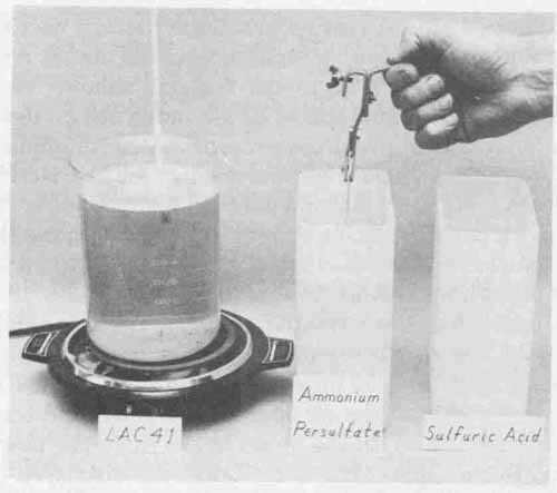
FIG. 5 Cleaning line (water rinses not shown.)
Step 4. An ammonium persulfate (AP) etching bath is the next phase of the cleaning cycle. This bath is prepared by adding 12 ounces of AP crystals to 2000 milliliters of warm water. To achieve uniform etching, it is absolutely essential that the board be slowly rocked back and forth continuously for approximately 30 seconds. A visual inspection of the conductor paths should show a smooth mat finish that is salmon in color. The proper operation of this micro- etch solution is critical to maintain good-quality boards. If the panel is left in this bath too long, the attack of the etchant solution on the hole walls will result in voids being generated. In the worst case, the entire 125-pinch thickness of copper on the barrels could be etched away. On the other hand, if the boards are not left in the bath long enough, the etch will not completely remove the photo- resist particles which may be locked into the copper. This would result in poor adhesion of the plated metal.
Step 5. The board is removed from this micro-etch bath and rinsed under a cold-water tap for at least 1 minute to remove the majority of the ammonium persulfate residue from the board surface.
Step 6. To remove all traces of ammonium persulfate residue and to neutralize the copper surfaces, the board is dipped into a diluted solution of sulfuric acid and rocked slowly for a minimum of 2 minutes to a maximum of 20 minutes (holding tank). This solution is prepared by adding 60 milliliters of CP sulfuric acid to 1940 milliliters of water. This mixture will yield a 3% by volume solution of sulfuric acid.
Step 7. After the final 3% sulfuric acid dip, the rack with the board is transferred directly into the plating tank for the copper pattern plating process.
It is recommended that all cleaning solutions used be prepared with either CP (chemically pure) or reagent-grade acids. In small quantities, all solutions used in the cleaning line should be changed daily to minimize the possibility of cleaning problems. The use of large quantities makes daily discarding and preparation time-consuming and economically unfeasible. To determine the effectiveness of the cleaning solutions and procedures, a modified water-break test should be used periodically. A test pc board (no pattern necessary) is passed sequentially through all the cleaning steps as outlined above. After the board is removed from the final sulfuric acid bath, the acid should “sheet” across the entire copper surface for a minimum of 30 seconds with no detectable “water breaks,” which is an indication of the presence of contaminants not success fully removed. A cleaning cycle that passes this test is effective in preparing the copper surfaces for quality plating.
The process for pattern plating copper employs the same plating tank and copper plating solution as described in Secs. 6 and 7, respectively. These sections should be reviewed before proceeding further.
After the board has been treated through the chemical cleaning and micro-etching baths, the rack is removed from the 3% solution of sulfuric acid. The board is then placed directly into the plating tank and the rack is secured to the cathode work rod with the air sparger activated and the power supply turned on to a low setting. With the board in the tank, the power supply may then be adjusted to the correct current setting. As discussed previously, the manufacturer’s recommendation for optimum current density is 30 amperes per square foot (= 208 mA/in. of copper area that is exposed to the plating solution. Recall that it was determined that the conductor patterns and thief areas on both sides of the preamplifier panel had a total copper surface area of approximately 20 square inches. The plating power supply setting is thus found according to the following relationship:
current setting = current density x total surface area
208 milliamperes/square inch x 20 square inches
= 4200 milliamperes =4.2 amperes
It will be noted that with the power supply set at 4.2 amperes, the output voltage is low (less than 1 volt) for this plating solution.
The required thickness of pattern-plated copper is an average of 1 mil. Plating thickness is a function of the current density and the plating time. The plating rate for varying current densities is shown in TABLE 4. Note that this table is based upon 100% cathode current efficiency. Because this is not practical, it has been found that the plating time listed in TABLE 4 should be in creased by approximately 25% to result in the specified plating thickness. For example, to obtain our specified copper thickness of 1 mil with a current density of 30 amperes per square foot, the ideal time of 35 minutes should be in creased by 1.25 to approximately 45 minutes.
TABLE 4 Plating Rate for Copper Sulfate Solution Based on 100% Cathode
Efficiency
After the panel has been plated, the power supply is reduced to a low set ting ( ampere) and the rack is removed from the cathode work rod. The board is immediately placed into a water rinse tank for at least 1 minute and then inspected for plating quality. There should be no pits, frostings, or hazy regions appearing on the imaged areas.
With copper pattern plating completed and the board rinsed, the panels are prepared for solder plating by dipping them into a 10% by volume solution of fluoboric acid at room temperature. This bath is prepared by adding 200 milliliters of concentrated fluoboric acid to 1800 milliliters of water and stirred. The panels should be slowly agitated for 1 minute in this bath. They are now ready for the solder pattern-plating process.
4. TIN-LEAD PLATING TANK AND ACCESSORIES
In the preceding section, the conductor patterns and thief areas of the pc board were pattern plated with an additional 1 mil thickness of copper in preparation for solder plating. Prior to the discussion of this plating process, however, the construction of a prototype plating tank will first be presented. You will note that this tank is similar to that used for flash plating and described in Sec. 17.6.
Because the tin-lead alloy will be electroplated from a fluoborate plating solution, the recommended material for the tank is stress-relieved polypropylene or polyethylene plastic. Glass-silicated materials or titanium are not suit able for fluoborate solutions and their use should be avoided.
A tank size of 12 inches long by 12 inches wide by 12 inches deep will be adequate for most prototype work. This tank will have a solution capacity of approximately 6 gallons when the plating solution is 9.75 inches from the bottom. As before, the exact volume can be calculated by dividing the number of cubic inches of solution by 231 cubic inches per gallon.
A 12-inch-deep tank with approximately 10 inches of plating solution (2 inches of clearance to the rim of the tank) will allow the insertion of the anodes and the racked pc board to be plated without causing the solution to spill over the top of the tank.
The tank is fitted with two anode work rods and one cathode work rod. The anode work rods are made of –inch diameter solid copper rod stock. This diameter will easily support the weight of the tin-lead anodes as well as handle the currents used. These anode work rods are held securely into position with pairs of Lucite or plastic blocks fastened onto opposite ends of the tank rim. The rods are positioned over the tank parallel to one another and 1 inch from the sides of the tank. The cathode work rod made from the same -inch-diameter copper stock is positioned parallel to the anode work rods and centered be tween them. The spacing between either anode work rod and the cathode work rod is 5 inches. The cathode work rod rests on a pair of plastic rollers attached to opposite ends of the tank rim and centered between the Lucite anode rod support blocks. This allows movement of the cathode rod parallel to the stationary anode rods. The cathode work rod must be capable of back-and-forth travel to provide agitation of the pc board in the plating solution. This type of rod motion will produce “knife agitation” of the racked pc board through the solution and is recommended for tin-lead alloy plating provided that the rate of motion is not violent. For tin-lead alloy plating, the recommended distance of travel of the pc board in the solution is from 3 to 6 feet in 1 minute. To realize this optimum range of travel distance, a high-torque motor operating at 12rpm is mounted to the tank rim. A drive wheel of approximately 2 to 3 inches in diameter is assembled to the motor’s shaft and the cathode work rod is linked to the drive wheel at a distance of 1 inch from the center of the motor’s shaft.
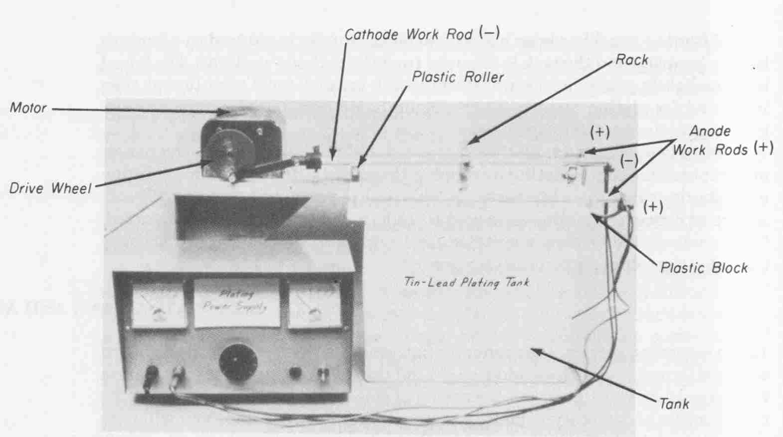
FIG. 6 Typical plating tank and accessories for tin-lead solder plating.
The linkage of the cathode work rod to the motor must be made with a nonconductive material, preferably plastic. As the motor rotates the drive wheel through one revolution, the cathode work rod will be pushed forward, pulled back, and then pushed forward again for a total distance of 4 inches. With a 12-rpm motor, the total distance traveled will be 48 inches or 4 feet in 1 minute. This distance is within the recommended range for “knife agitation” used for tin-lead alloy plating. A typical plating tank fabricated as described in this section is shown in FIG. 6.
The negative terminal of a plating power supply is electrically connected to the cathode work rod. Both anode work rods are electrically connected together (anode strap) and then connected to the positive terminal of the power supply. All electrical connections should be made with AWG No. 12 stranded wire protected with a chemical-resistant plastic insulation.
The plating power supply should have the same characteristics as that used for flash plating as described in Sec. 17.6. It can, however, have a lower current rating since pattern plating requires much less current than does flash plating the entire panel area.
The type of material used for the anode, together with its shape and surface area, will affect the quality of the alloy that is plated onto the pc board. Because the tin—lead alloy to be plated requires a metal ratio of 60% tin and 40% lead, anodes with this same ratio should be utilized. The anodes must also be free of oxides and have low metal impurities. Anode material that meets all these specifications is high-purity Vaculoy. Anodes made with this material will corrode evenly in the plating solution, produce less sludge, and improve bath stability.
Recall from Sec.6 and Fig. 13 that the standard anode shapes are flat, oval, round sawtooth, and gear tooth. For prototype applications, the flat configuration is preferred. The criteria for selecting an anode is its surface area relative to the area of the pc board to be plated. For the plating of tin-lead alloy, an anode-to-cathode surface area ratio of approximately 2:1 is recommended. This means that the surface area of the anode facing the pc board in the plating tank should have a surface area approximately twice as large as the one side of the board it is facing. You will recall from Section 16 that uniform plating on double-sided pc boards will result if the overall exposed conductor path area is made to be equal on both sides of the board. Double-sided plating is accomplished with the use of two anodes, one positioned on each side of the pc board, both having identical surface areas. This will simplify and optimize the plating process and a uniform coating of 60/40 tin—lead alloy will be plated on both sides of the pc board.
The anodes must be provided with a hook whose length will allow the anode to extend from the anode work rod down into the plating solution yet allow the top of the anode to protrude slightly above ( inch) the surface of the solution. The length of the anode should be such that it extends from 1 to 2 inches below the bottom edge of the pc board, which is suspended from the cathode work rod. This will result in a higher current density on the thief area of the pc board and tends to improve the uniformity of alloy composition in the conductor-path area. Thus the two restrictions which are placed on the selection of the anode size is that (1) it has a surface area from one to two times larger than that of the pattern facing it and (2) it is from 1 to 2 inches longer than the pc board bulk stock. We will again use the preamplifier panel to select the correct anode size for solder pattern plating. Recall that the exposed conductor pattern and thief area on each side of the 5- by 5-inch card is 10 square inches.
First, an anode is selected whose length is 6 inches (1 inch longer than the 5-inch bulk stock). If the anode width is chosen to be 4 inches, the anode surface area will be 6 inches x 4 inches = 24 square inches, which is within the range of from one to two times larger in area that the area of the pattern to be plated. Since each side of the preamplifier layout has approximately equal areas, two 4- by 6-inch anodes will meet all of the requirements for plating the preamplifier pc board.
Prior to the placement of the anodes into the plating tank, proper procedures must be followed to avoid contaminating the plating solution. Tin-lead fluoborate plating solutions are extremely susceptible to organic contaminations. For this reason, the anodes must be properly cleaned and correctly bagged. Anode degreasing is accomplished by scrubbing the surface with a brass bristle brush and cold tap water. The anode is then rinsed thoroughly and dipped into a 15% by volume solution of fluoboric acid for approximately 10 minutes. After the acid dip, the anode is ready to be bagged.
The anode bags used should be made of either polypropylene or dynel (but never cotton) and should be 2 inches wider and 2 inches longer than the anode. The bag must be leached (purified) of all organic contaminations that it was exposed to in its manufacturing process. Leaching is accomplished by boiling the bag in water for at least 1 hour at 150°F (66°C). The bag is then removed, rinsed in cold water, and tied around the cleaned anode. The anodes are now ready to be installed into the plating tank. Recall that the anode cleaning and bag leaching procedure is similar to that used for the anodes and bags in the copper plating process discussed in Sec. 6.
In addition to the anode preparation, the plating tank itself must be thoroughly leached of all contaminations prior to the addition of the plating solution. Tank leaching should be done with all the hardware and electrodes removed from the tank. Leaching of the tank need be done only before the plating solution is added to the tank for the first time.
(cont. >>) .