AMAZON multi-meters discounts AMAZON oscilloscope discounts
cont. from part 1
Single- and double-balanced systems:
All of the mixer circuits so far described are commonly known as single-ended systems, in which there are single signal and oscillator ports. This type of layout can be elaborated into push-pull systems, de scribed as 'single balanced' and 'double balanced' layouts. These offer a better conversion efficiency -- and consequently an improved s/n ratio -- as well as improved port to port isolation: this factor is better with dual- than with single-balanced types.
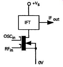
FIG. 25 Dual gate MOSFET mixer
The simplest single-balanced system is that using a diode bridge layout, shown in FIG. 26, where the oscillator signal is injected into the centre tap of the secondary winding on a wide-band RF transformer--usually 'tri-filar' wound on a toroidal ferrite core. This layout gives good oscillator to input, but poor oscillator to output isolation. Diode mixers of this type can give excellent performance in respect to cross-modulation and input overload, but need a high oscillator output voltage at a low source impedance, and suffer from the drawbacks of both a conversion loss and a relatively poor noise figure.
A double balanced diode layout, often called a 'ring mixer', is shown in FIG. 27. This gives good port-to-port signal isolation, and excellent IM and cross-modulation characteristics. Using 'hot carrier' or 'Schottky-type' (metal/semiconductor junction) diodes, this layout is usable up to the UHF (gigahertz) range.
Single and double-balanced mixer layouts using MOSFETs and junction FETs are shown in FIGs 28-30.
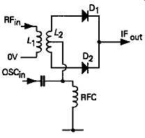
FIG. 26 Diode bridge single-balanced mixer.
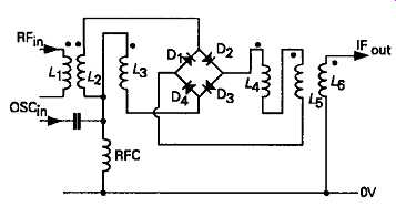
FIG. 27 Double-balanced ring mixer.
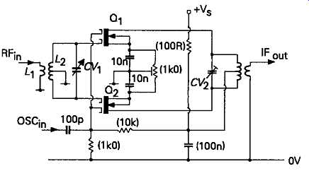
FIG. 28 Single-balanced mixer using.
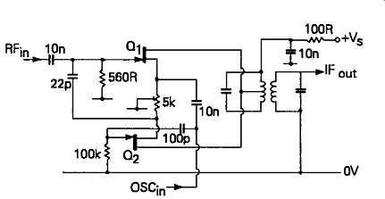
FIG. 29 Balanced mixer using junction FETs.
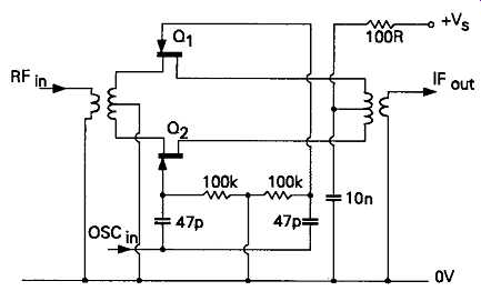
FIG. 30 Low noise balanced mixer based on junction FETs.
Oscillator stages:
A number of circuit designs which could be used as the local oscillator in a superhet have been described in Section 13. The important considerations in this particular application are that they should be stable in frequency, and have a low noise and spurious signal content in their output waveform.
Temperature compensation:
The importance of frequency stability is dependent upon the degree of selectivity of the receiver, and the tolerability of tuned frequency drift with time. Most LC tuned circuits will suffer from drift as a result of changes in the ambient temperature of the oscillator circuit, though, with low power solid-state circuitry, 'warm-up' frequency drift following switch-on is no longer a particular problem.
Some compensation for thermal drift in LC oscillators can be achieved by the incorporation within the tuned circuit of additional capacitors having a negative or positive temperature coefficient. These may simply be connected in parallel with the tuning capacitor, and would typically be of metallized ceramic construction.
Such capacitors are usually designated N- or P-, with the coefficient specified in parts per million per degree Celsius. For example, an N-750 marking would denote a temperature coefficient of -750 parts/million/°C, and a P-100 one a capacitor with a +100 ppm/°C characteristic. Similarly a NPO marking would imply a near zero temperature coefficient for the component. Choosing the correct value and type of temperature compensation components is usually a laborious and tiresome exercise, especially if compensation over a wide temperature range is sought.
A high degree of oscillator frequency stability is particularly desirable in the case of receivers designed to receive CW signals (transmissions consisting of a simple sinewave carrier, interrupted by morse or other coded keying patterns), where the signal is made audible by a beat frequency oscillator (BFO) stage.
This operates by heterodyning the signal, in a further mixer stage, with an oscillator having an adjustable output frequency close to that of the IF. In this case a shift in incoming signal frequency due to oscillator drift will result in an audible change in the BFO pitch.
Oscillator frequency drift will also be embarrassing where the receiver is used to receive a 'suppressed carrier' signal, where if the reinserted carrier frequency moves away from the desired frequency, the received signal may become unintelligible.
The freedom of a local oscillator output from spurious signals is obviously necessary if whistles and the reception of signals at unwanted frequencies is to be avoided, and this demands care in the layout of the resonant LC circuit, to avoid inadvertent inductive loops, or inconvenient stray capacitances.
The requirement for a good signal-to-noise ratio in the local oscillator output arises because any modulation component of the local oscillator output, such as noise, will be added to the output sum and difference signals, in just the same way as the modulation present on the carrier of the wanted signal. So, if a 60dB signal-to-noise ratio is required for an input signal of 10µV amplitude then the local oscillator signal must have a signal-to-noise ratio of at least 80dB. Also, in some cases, mixer nonlinearities may exaggerate this problem by increasing the extent to which local oscillator noise is added to the composite signal.
IF amplifier stages
The basic requirements for both RF and IF amplifier stages are the same -- that they should give a useful degree of gain, a high signal-to-noise ratio, an adequate input linearity (to avoid cross-modulation), and that they should be stable in operation. However, whatever the means by which adjacent signal selectivity is obtained, the fixed frequency IF stages have the advantage that they won’t usually require tuning except in setting up the receiver. Any of the HF filter systems examined in Section 11 can be employed, and two typical IF amplifier blocks in which the selectivity is defined, in the first case by a group of four band pass-coupled tuned circuits, and, in the second instance by a surface acoustic wave ladder filter, are shown in FIGs 31 and 32.
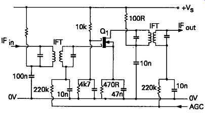
FIG. 31 IF amplifier stage using bandpass coupled tuned circuits. AGC
FIG. 32 IF amplifier using ceramic SAW ladder filters
Automatic gain control (AGC)
An inevitable difficulty with the reception of amplitude modulated signals is that the larger the signal, the larger the demodulated audio frequency output. This means not only that strong signals will be louder than weak ones, which will necessitate continuous adjustment of the receiver output gain control as it’s tuned from one signal to another across the band, but also that fluctuating signal strength, due to changing reception conditions, will lead to 'fading'. Because of the very high IF gain which is usually available, it becomes possible with superhets to derive a further signal-dependent voltage, proportional to the average magnitude of the received carrier, and use this voltage as a gain control mechanism, to reduce the gain of the IF stages (and usually, also, the RF stages if used) to try to ensure that the magnitude of the IF signal presented to the demodulator is of a substantially constant size.
A simple AGC circuit is shown in FIG. 33, in which a negative gain control voltage, suitable for controlling the gain of a valve or MOSFET/FET operated IF amplifier, is derived from a diode demodulator.
Some HF filtering is necessary in the AGC loop to avoid HF instability due to signal feedback, but the time constants for the gain control circuitry must be chosen with care, since too long a response time in the control system will reduce its ability to correct rapid 'flutter type' fading, while too short a time constant will attenuate the lower modulation frequencies, which will be interpreted by the AGC system as un wanted fluctuations in signal strength.
It must be remembered also that the gain control system is a closed loop servomechanism, and if the accumulated phase shifts in the control loop approach 180°, the whole system may become unstable, leading to the problem known, from its sound, as 'motor boating'.
To avoid needlessly reducing the gain of very weak signals, it’s common to arrange the design so that there is a lower threshold level in the AGC control system, below which the AGC voltage won’t be applied. This is usually termed 'delayed AGC'. Similarly, to in crease the effectiveness of the AGC system, designers may sometimes employ a DC amplifier in the AGC loop. A low distortion demodulator system, using both amplified and delayed AGC, is shown in FIG. 34. (JLH, Wireless World, October 1986, p. 17).
Signal demodulation:
Most of the demodulator systems described above in relation to TRF type receivers will operate quite satisfactorily as the demodulator, or 'second detector' in a superhet. However, since there is almost always an adequately large IF output signal available, and the designers of AM receivers are seldom concerned about minimizing demodulator distortion, a simple diode demodulator, of the kind shown in FIG. 33, is nearly always used.
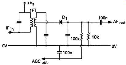
FIG. 33 Automatic gain control voltage generation circuit
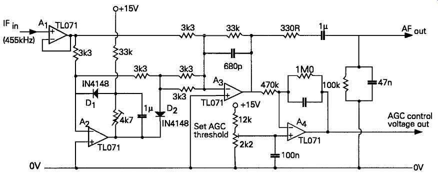
FIG. 34 Low distortion demodulator incorporating amplified AGC
Stable frequency oscillator systems
The use of high signal frequencies in receiver or oscillator systems exaggerates the problems of frequency drift, simply because the same proportional drift becomes a higher frequency error at higher frequencies. For example, a 0.01% drift at 100kHz will be 10Hz -- a negligible amount in most applications.
However, the same proportional drift at 100MHz will be 10kHz -- an error which would be unacceptable in almost every case. A relatively simple solution to this problem, provided that the coverage of the receiver is relatively limited, is to use a fixed frequency, quartz crystal controlled, local oscillator, coupled with a tunable IF. This would, however, suffer from the drawback that if the chosen, tunable, IF was low enough not to suffer from frequency drift, there would be a problem due to second-channel breakthrough, due to inadequate RF selectivity, while if the chosen IF was high enough to avoid this problem, the IF stage -- which would also be a superhet receiver -- would also suffer from frequency drift.
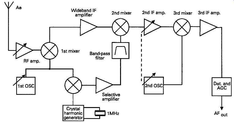
FIG. 35 The Barlow-Wadley loop drift cancelling oscillator system [Wideband
IF, amplifier; 2nd mixer 2nd IF amp. 3rd mixer 3rd IF amp.]
A number of systems have been evolved to reduce the extent of this problem, of which the two most interesting, in that they represent entirely different, and original, design philosophies, are the Barlow Wadley drift cancelling loop, and the phase-locked loop frequency synthesizer system.
The Barlow-Wadley drift cancelling system:
The way this system works is shown, in schematic form, in FIG. 35. In this the aerial signal, amplified by a conventional tuned RF stage, is fed to a first mixer, along with the output signal from a good quality LC tuned local oscillator, operating at a frequency which is above that of the incoming signal. The resulting first IF signal is then amplified at an IF frequency of, say, 45MHz and fed to a second mixer stage.
Because of the inevitable frequency drift in the first local oscillator stage, the 45MHz IF output will also suffer from drift. However, attached to the oscillator system is a stable frequency quartz crystal oscillator, operating at, say, 1MHz, and the output from this is fed to a harmonic generator circuit, to produce an array of output frequencies, at 1MHz intervals, extending up to, say, 100MHz or more. This harmonic series is then mixed with the output of the first variable frequency LC oscillator, and the composite output from this mixer is fed to a selective amplifier tuned to a frequency which is higher than the 45MHz first IF, by an amount equal to that of the second (say, 3MHz) IF amplifier. The output signal from this will suffer from an identical frequency drift, and in the same direction, as that of the first IF output signal, and the resultant eiTors will cancel, giving a drift-free input to the second IF amplifier/demodulator combination.
As an elaboration of this basic principle, the first IF can be chosen to have a fairly wide, flat-topped frequency pass-band, and the second IF stage can then be made tunable over, say, the 2-3MHz range, to provide a band-spreading facility for the receiver -- since frequency drift in a 2-3MHz receiver will seldom be a major problem. The first variable frequency oscillator can then be used to select the incoming signal frequency in 1MHz blocks.
Frequency synthesizer techniques:
These can be divided into 'partial' synthesis and 'full' -- i.e. 'digital' -- synthesis designs. The partial synthesis method combines a quartz crystal oscillator with a standard LC variable frequency oscillator (VFO), as, for example, in the simple circuit arrangement shown in FIG. 36. In this a receiver designed to cover the frequency range 28-30MHz, with a first IF frequency of 10.7MHz, employs a VFO tunable over the frequency range 1.7-3.7MHz. The output from this is heterodyned with that from a 37MHz quartz crystal, and passed through a 38.7-40.7MHz selective amplifier, before being mixed with the aerial signal in the receiver. This technique is adequate for coverage of a limited and specified waveband, but would require that a range of crystals were available to allow tuning over a wider input signal range. Full frequency synthesis techniques rely on the use of a phase-locked loop (PLL), for the control of the oscillator, so I propose to explain this system first.
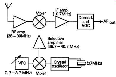
FIG. 36 28-30MHz receiver system.
The phase-locked loop:
This circuit arrangement, shown in schematic form in FIG. 37, provides a powerful technique for forcing a variable frequency voltage controlled oscillator (VCO) to operate at a specified frequency, as well as a means for deriving a DC voltage output related to this frequency, if this should be needed.
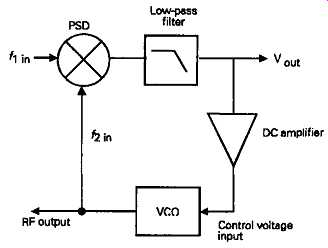
FIG. 37 The phase-locked loop
In the simple circuit arrangement of FIG. 37, the PLL consists of just four elements, an input mixer or 'phase sensitive detector' (PSD), a low-pass filter, a DC amplifier, and a voltage controlled oscillator, whose output frequency is determined by the control voltage applied to it. If the free-running frequency of the VCO is close to that of the input signal, and if it’s postulated that, momentarily, the input frequency (ft), is the same as the VCO output frequency (ft), the PSD output will be a DC voltage which is related to the phase difference between these two signals. If this is amplified, and applied to the input of the VCO, it will cause this oscillator to speed up, or slow down, over part of a cycle, in such a manner that f1 and f2 are brought into phase and frequency synchronism with one another. If the free-running frequency of the VCO is truly that which requires a zero DC control voltage, then ft and/2 will also be at phase quadrature, since that is the condition at which the PSD will have a zero voltage output, and if the loop amplifier has a high enough gain, a near-quadrature phase relationship be tween the signal and the VCO will also be the condition for non-zero VCO control voltages. Moreover, it’s also found that if f_t and f2 are not initially identical, then, provided that the difference frequency is within the pass-band of the low-pass loop filter, known as the capture range, then the VCO will be drawn into, and will remain, in synchronism with the input signal. This is described as the PLL being in lock'.
If a frequency divider is incorporated in the VCO/PSD loop, then the VCO can be forced to oscillate at a multiple of the input frequency. Similarly, if a frequency divider is introduced into the control frequency path (ft), then the VCO can be caused to oscillate at a sub-multiple of f_t.
The choice of filter bandwidth is dictated by the required capture range, and the required purity of the VCO output, since increasing the bandwidth of the filter increases the amount of wideband noise which will be added to the control voltage.
Digital frequency synthesis techniques:
The complete superhet receiver shown in outline in FIG. 38 uses an elaboration of the frequency multiplication, frequency division possibilities of the phase-locked loop circuit to generate a fully variable, but crystal-controlled, local oscillator frequency.
In this, a crystal controlled oscillator, operating at a frequency f0, is used as a reference frequency generator, whose output is frequency divided by a factor of n, before introduction as the control signal, f, to the PSD. The output from a high frequency voltage con trolled oscillator is also divided before being applied to the PSD, and the PSD output is filtered and amplified before application as the control voltage to the VCO. Then, when the PLL is in lock, the output from the VCO, f3, will be determined by the crystal frequency according to the relationship …and will be very stable in frequency. By the use of a microprocessor to control the two division ratios, the required input signal frequency of the receiver shown in FIG. 38 can be controlled by receiver front panel push-button selection, and the selected signal can be shown, for convenience, on a digital frequency display.
A number of manufacturers now offer single-chip frequency synthesizer ICs, which greatly facilitate the use of this technique.
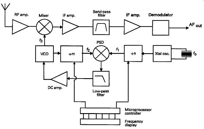
FIG. 38 Complete superhet receiver using frequency synthesized local oscillator
system.
Synchrodyne and homodyne receiver systems:
The difficulty of achieving adequate selectivity with TRF type receivers, and the many technical problems associated with superhet systems, has prompted exploration of the possibilities of direct conversion receivers, of the kind discussed above. The advantage of a direct conversion receiver, if the local oscillator frequency can be controlled so that it’s truly identical to that of the carrier of the received signal, is that demodulation of the incoming signal will occur with out the need for a specific demodulator circuit: the input sum and difference frequencies produced by the amplitude modulation of the carrier will be directly transformed into an audible signal. This avoids the problems of poor demodulator sensitivity and linearity. Moreover, since the sidebands of adjacent interfering signals will also be transformed into audio signals, but of a much higher pitch, the receiver selectivity can be provided by post-mixer AF filtering, for which there are a number of useful low-pass filter circuits, as shown in Section 8. The only problem with this system is that if the pre-mixer selectivity is inadequate, cross-modulation can occur at the input to the mixer, to introduce an interfering signal which is proof against subsequent attempts at removal.
The difficulty, obviously, is to generate a local oscillator signal which is truly in synchronism with the required aerial signal. In the homodyne circuit, best implemented as the demodulator system for a broad selectivity superhet, a solution to this problem is at tempted by using the carrier of the desired signal for this purpose, as shown in FIG. 39. In this, a very narrow bandwidth IF stage, in parallel with the normal IF amplifier, is used to generate a signal, derived from the input signal carrier, but amplitude limited to remove its modulation component, which can be employed to synchronously demodulate the incoming signal. This system does work, but small changes in the signal tuning will alter the relative phases of the two signals applied to the mixer, and this will substantially alter the magnitude of the audio output from the mixer.
In the synchrodyne receiver, it’s also required that the local oscillator signal fed to the mixer is synchronous with the wanted signal. An attempt is usually made to satisfy this requirement, in simple systems, by introducing a small amount of the aerial signal into the local oscillator circuit. If the local oscillator frequency should drift away from the signal frequency, the loss of synchronism becomes audible as a loud whistle, whose pitch is determined by the difference frequency, and this fact, especially noticeable when tuning from one signal to another, coupled with the difficulty of maintaining synchronism of the local oscillator, has prevented the use of this technique on anything other than a laboratory scale. However, a synchrodyne receiver design in which phase-locked loop techniques were used to force the local oscillator into phase and frequency synchronism, and in which inter-station muting was incorporated, is shown in outline in FIG. 40. A practical receiver based on this structure was described in Wireless World. (JLH. Jan. 1986, pp. 51-54, Feb. 1986, pp. 53-56 and March 1986, pp. 58-61).
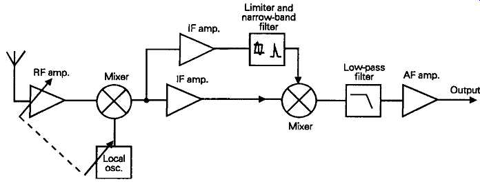
FIG. 39 Circuit arrangement of homodyne receiver. Limiter and narrow-band
Frequency modulation (FM), systems:
In this type of transmission system, the frequency, rather than the amplitude, of the transmitted signal is modulated to carry the program content. This idea, also, was due to the same remarkable Major Edwin Armstrong who invented the concepts of positive feedback, regeneration, the super-regenerative and the superhet types of radio receiver.
As a broadcasting technique, FM has many advantages, of which the major ones are that, since the amplitude of the received signal is now no longer important, all of the incoming signals can be amplified sufficiently to allow their amplitude to be limited by a clipping stage, such as the simple back-to-back diode limiter shown in FIG. 41. This has the immediate practical benefit that signal fading is eliminated, and that all incoming signals are received at the same volume level. In addition, 'frequency discriminator' demodulation systems are, at least potentially, very much better in terms of linearity, and freedom from signal distortion, than comparable AM demodulators.
They will also, in good designs, give a high degree of rejection of 'impulse type' noise, such as that caused by electrical switch contact interference and motor vehicle ignition noise. Rejection of interfering adjacent channel signals is also assisted by the 'capture' effect, a feature of the demodulator system employed, in which the presence of a stronger signal, at the demodulator, will completely suppress a somewhat weaker one: the extent to which this occurs is known as the 'capture ratio'. Good FM demodulator circuitry can offer capture ratios better than 1dB. The major drawback of FM broadcast systems is that, for optimum modulation bandwidth and linearity they require a very wide transmission bandwidth. Peak modulation bandwidths of +/-75kHz are typical of contemporary FM broadcast transmitters, for which good quality reception requires a receiver bandwidth of at least +/-120kHz. Clearly, this amount of broad cast bandwidth is not available in the existing and crowded long- or medium-wave commercial transmission bands, so a part of the frequency spectrum between 88MHz and 108MHz has now been set aside, by international agreement, for domestic FM broad cast transmissions. The use of this part of the RF spectrum offers both advantages and disadvantages, in that the general absence of significant ionospheric reflection means that reception will only be possible, normally, over line-of-sight distances. So, for general reception, a network of local stations is necessary, and the choice available to the listener is usually restricted to the programs broadcast on his or her own national network. On the other hand, the limited range of transmissions in this frequency band eliminates over crowding, and the likelihood of unwanted adjacent channel interference.
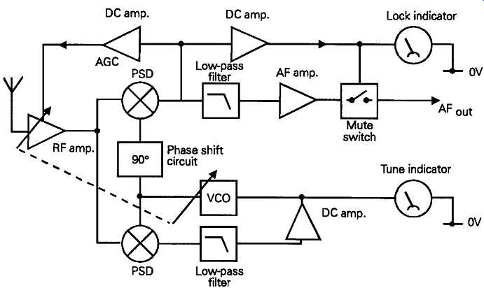
FIG. 40 Synchrodyne receiver
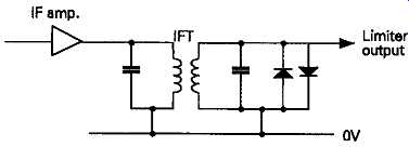
FIG. 41 Simple diode amplitude limiter circuit
FM receiver design FM demodulator systems The design of receiver used for FM reception usually follows conventional radio practice, only modified as necessary to suit the 88-108MHz signal spectrum, and the required IF bandwidth. The frequency normally used for the IF is 10.7MHz, and a wide range of piezo-electric ceramic surface acoustic wave (SAW) filters is available, allowing substantially flat-topped response curves, with a range of bandwidths, for different applications.
Contemporary 'tuner head' design practice favors either dual-gate MOSFET, or neutralized junction FET stages, with similar devices for the mixer stage.
Since varicap diode tuning allows additional tuned circuits to be added without practical difficulties, it’s common, in better class tuners, to find three or four tuned circuits preceding the mixer, to reduce cross modulation effects, and improve the effective s/n ratio.
A typical layout for a varicap tuned FM RF/mixer circuit is shown in FIG. 42, and a 10.7MHz IF stage, using ceramic SAW filters, is illustrated in FIG. 32.
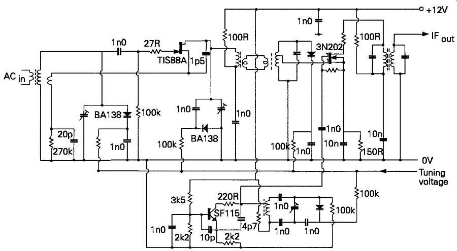
FIG. 42 Commercial FM tuner head design.
The slope detector:
Various methods have been adopted, over the years, as a means for converting a constant amplitude RF signal which varies in frequency into a varying DC output voltage level. Of these, the simplest, and most straight forward, is to feed the signal to a diode detector, coupled to a tuned circuit, whose natural resonant frequency is displaced somewhat to one side of the signal frequency, as shown in FIG. 43. This will somewhat distort the demodulated signal, as shown, because of the curvature of the tuned circuit resonance curve. It will also offer no immunity from AM signal breakthrough or impulse-type interference.
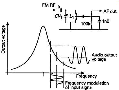
FIG. 43 Simple FM 'slope' demodulator
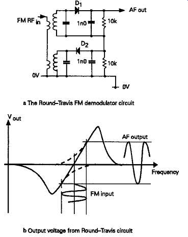
FIG. 44 --- b Output voltage from Round-Travis circuit
The Round-Travis circuit:
An improvement in this arrangement is offered by the 'Round-Travis' layout, shown in FIG. 44, in which two such demodulator circuits are connected with their outputs in series, with one tuned somewhat above, and the other tuned somewhat below the mid point signal frequency. The effect of adding the two resonance curves is to improve the overall demodulator linearity.
The Foster-Seeley discriminator:
The most important improvement in the effectiveness and linearity of the FM demodulator was the introduction of the 'Foster-Seeley' circuit shown in FIG. 45. The operation of this is based on the fact that the phase of the voltage developed across a tuned circuit, which is loosely coupled to an input winding, will be at quadrature (90° or 270°), to that of the input signal when the tuned circuit is at resonance. This leads to the possibility that, if an input signal is injected into the centre tap of the resonant circuit, it will either add to the output voltage or oppose it, depending on the input frequency, and this circuit will give a very linear output voltage/input frequency relationship for relatively small input signal voltages.
The Foster-Seeley discriminator ; Frequency/voltage characteristics of Foster-Seeley circuit.
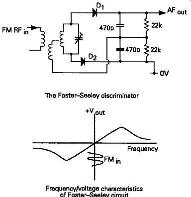
FIG. 45
The major practical drawback with this layout is that it offers very little discrimination against impulse-type AM breakthrough, a persistent problem with VHF reception due to the prevalence of motor vehicle 'ignition noise'.
The ratio detector:
The circuit known as the 'ratio detector', shown in FIG. 46, minimizes this problem by connecting the two demodulator diodes in opposition, so that the output is the ratio between the two signal voltages rather than their sum. It’s not, however, either as efficient or as linear in its demodulation characteristics as the Foster-Seeley discriminator.
Contemporary design practice favors, almost exclusively, the use of a quadrature coil 'gate coincidence' demodulator (GCD) combination, shown in FIG. 47, because this can easily be fabricated as part of a monolithic IC structure. Since these ICs, such as the RCA CA3189, also offer a host of other useful functions, such as gain control, automatic frequency control, signal strength indication and off-station noise 'muting', it’s understandable that they are widely used.
The GCD is a true phase-detector, in that there will be no output voltage change if an input signal voltage is applied to either of its signal ports, on it own, or if two input voltages arc applied in phase quadrature --which would be the case if the quadrature coil, L1/C1 is resonant at the incoming frequency. If the input frequency is altered, there will be a change in the output voltage level which, over a limited voltage range, will be as linear as the output from a Foster Seeley discriminator, but with improved AM rejection. Typical THD values for a single quadrature coil GCD design lie in the range 0.8-1.5% THD for a +/-75kHz modulation level. By comparison, an AM demodulator would give 2-5% THD for a 50% modulation level.
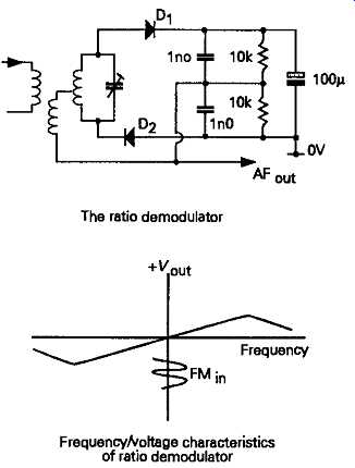
FIG. 46 --- The gate coincidence demodulator---The ratio demodulator, Frequency
A cottage characteristics of ratio demodulator
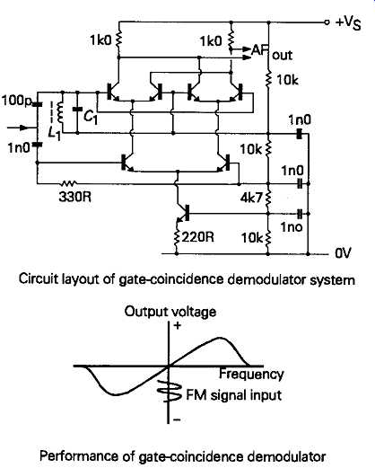
FIG. 47 --- Circuit layout of gate-coincidence demodulator system; Performance
of gate-coincidence demodulator.
It’s claimed by the manufacturers of gate coincidence demodulator ICs that the linearity of the de modulator system can be improved to allow better that 0.1% THD distortion levels, by coupling a further resonant tuned circuit to the quadrature coil. This configuration remains more of a theoretical possibility than a commercially valuable system because the out put distortion given by this arrangement depends critically upon the coupling factor between these two tuned circuits. If they arc 'under coupled' little benefit is given, while if they are 'over coupled', the demodulator output will show a pronounced crossover distortion type kink at the mid-point frequency (JLH, Wireless World, March 1991, p. 220).
Phase-locked loop demodulator systems:
The circuit layout shown in FIG. 37 can also be used to provide a very efficient, low distortion FM demodulator system, in that if the loop is locked, the frequency of the voltage controlled oscillator will be identical to that of the input signal. If this varies in frequency, the DC output from the loop (point 'B' in the figure) will be that which is required by the voltage controlled oscillator to cause it to oscillate at that frequency. If there is an accurately linear relationship between the VCO control voltage and its output frequency, then an input FM signal, applied to point 'A' will also be demodulated, by this means, at point 'B?', with very little modulation distortion. Such a PLL demodulator will also give very good AM rejection and an excellent capture ratio. As a matter of personal interest, I have designed a number of experimental FM receivers using this system, of which the most recent was offered as an amateur constructional project in 1987 (JLH, Electronics Today, March 1987, pp. 34 38).
Automatic frequency control (AFC):
One of the inherent advantages of any FM demodulator is that the signal output is a DC voltage which is related to the incoming signal frequency. If this varies, the output voltage will change. With tuner circuits using varicap diodes, this DC output voltage can be applied to the oscillator tuning system so that un wanted drifts in the tuned frequency can be corrected.
This is a particularly valuable feature in receivers operating at such relatively high signal frequencies, so that most commercial tuner head designs provide an AFC input control point, for direct connection to the AFC output from the demodulator IC.
Inter-station noise muting:
With FM tuner designs in which a high signal amplification level is coupled to an amplitude limiting clipping stage, all signals, including the thermal noise input from the aerial, or that due to the input stages to the receiver, will be amplified to the clipping level.
Moreover, since the thermal noise will have a random distribution in both amplitude and frequency it will be demodulated into a wideband (white), noise signal, and this is a disconcerting feature in inexpensive FM receivers without automatic inter-station muting facilities.
Various techniques are used to mute this noise, of which the simplest is to monitor the IF signal strength, at some point prior to the limiter stage, and arrange the circuit to switch off the audio output if the measured signal level falls below some predetermined value. A circuit for this purpose is shown in FIG. 48.
FIG. 48 Inter-station muting circuit for FM receiver
A rather more sophisticated approach, employed by RCA in their CA3189 IC, is to monitor the extent of signal frequency deviation, and mute the output if this exceeds a certain value, as it will do with a wideband noise input.
FM Stereo broadcast transmissions:
The extra modulation bandwidth available on the Band ? region of the VHF allocated for FM broadcasts has been exploited to allow stereo broadcasting, using the GE-Zenith 'pilot tone' system, for which the band width distribution is as shown in FIG. 49. In this a normal 'L+R' mono signal is transmitted, using the 30Hz-15kHz part of the modulation spectrum, while an additional 'L-R' signal is broadcast as a double sideband supersonic signal based on a carrier frequency of 38kHz, giving a maximum modulation for the composite (L+R/L-R) signal of 90% of the per mitted +/-75kHz deviation. This 38kHz carrier is suppressed before transmission to avoid unwanted breakthrough into the normal audio passband, and is then reconstructed, in the 'stereo decoder' of the receiver, from a phase synchronous 19kHz pilot tone broadcast at 10% effective modulation depth. This technique is 'mono compatible' in that, on FM receivers without stereo decoding facilities, the signal is received as a normal mono broadcast, whereas, on suitably equipped receivers, a pair of separate, low distortion, 'L' and 'R' channel outputs, having up to 40dB channel separation, are provided. Decoding this composite signal can be effected by treating the L-R signal as a normal LF radio signal and, after separating the carrier from the L+R signal, demodulating it in a conventional way to give a L-R output, from which the separate L and R signals are obtained by subtraction or addition. Alternatively, the L and R outputs can be obtained by synchronously switching the composite signal between the two channels, at a 38kHz frequency -- a process which effectively does the same job.
These alternative decoding techniques are illustrated schematically in FIG s 50 and 51.
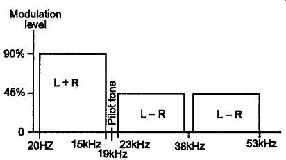
FIG. 49 The carrier modulation characteristics used in the GE-Zenith FM stereo
transmission system
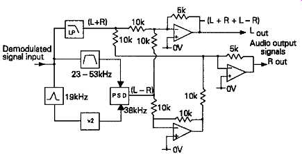
FIG. 50 Matrix stereo decoder system
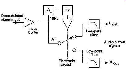
FIG. 51 Switching type stereo decoder
Appendix: Transmission and reception data
There are a number of terms which are conventionally used in the classification of radio broadcast signals.
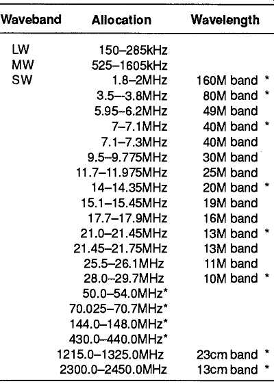
Those relating to the frequency spectrum are listed in TBL. 1.
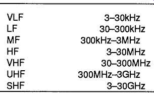
TBL. 1 Classification of radio frequency bands
TBL. 2 Broadcast band allocations
(* denotes amateur transmitter frequency allocations).
Within these frequency bands segments have been allocated, by international agreement, for domestic and amateur usage, as shown in TBL. 2.
Note. It’s observed that not all national/commercial broadcasting authorities adhere strictly to these frequency allocations.)
In addition to these allocations there are other VHF/UHF band designations, listed in TBL. 3.
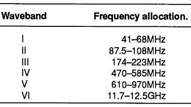
TBL. 3 VHF/UHF Frequency band designations
Recent changes in the internationally agreed transmitter frequency separation in the LF and MF bands have imposed constraints on the broadcast bandwidth, in order to limit adjacent channel sideband interference. VHF broadcasts are not subject to these constraints, and can therefore provide a wider program frequency range.
Details of the British broadcast standards, published by courtesy of the BBC, are listed below.
Audio bandwidths
LF/MF(AM)
40-5800Hz +/-3db (cut-off rate >24dB/octave
beyond 6kHz)
50-5000Hz +/-1db
VHF(FM)
30Hz-15kHz +/-0.5dB (Cut-off rate >24dB/octave
beyond 15kHz)