AMAZON multi-meters discounts AMAZON oscilloscope discounts
Introduction
Although I have used the term Radio in the section heading, the basic techniques and systems which are used for radio reception are much the same as those employed in television, Radar, radio astronomy, and other systems used to receive high frequency electro magnetic radiations, apart from any modifications to the receiver which may be needed to meet the specific requirements of the operating frequency, or the signal bandwidth.
For me, and perhaps for many others of my generation, radio circuitry has always enjoyed a special degree of affection because it was my original introduction to the whole field of electronics, and I still think that there are two uniquely enthralling pleasures of revelation which await the practically minded- that of watching a black and white print image, of ones own, appear, for the first time, in the developing dish in a photographic darkroom, and that of hearing ones first shortwave radio signals, on headphones, on a home-built radio receiver. Of these two pleasures, that of radio has the advantage that, with care, all of the components are re-usable. One does not need to throw away ones failures, one can dismantle them, instead.
Radio receiver circuitry
Tuned radio frequency (TRF) systems
Demodulation methods:
In most radio signals, the amplitude of the high frequency, (HF or RF), transmitted waveform, usually called the carrier, is modulated, (caused to vary), as a means of carrying the lower frequency information or program content of the transmission. With a high frequency signal, the fluctuations in the amplitude of the incoming signal would be far outside the audible range, and undetectable. In order to allow the receiver to convert such an amplitude modulated (AM) RF voltage into an audible or measurable signal, the process known as demodulation or detection is used, most commonly by simply rectifying the incoming RF waveform, shown in FIG. 1a, to give a waveform of the kind shown in FIG. 1b. If this voltage waveform could be averaged, as shown in FIG. 1c, the result would be a true replica of the original waveform used to modulate the carrier. Unfortunately, the easiest technique for doing this, just to use a resistor/capacitor/diode circuit, of the kind shown in FIG. 2, leads to a substantial distortion in the recovered modulation waveform, as shown in FIG. Id, unless the CR discharge time constant is kept short in relation to the highest modulation frequency employed, and this lowers the demodulation efficiency.
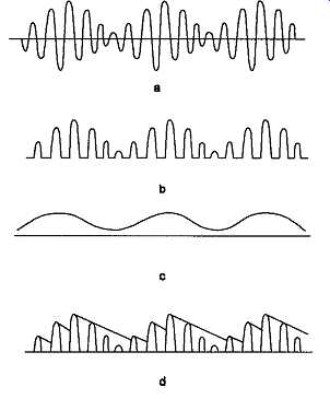
FIG. 1 Action of diode demodulator.
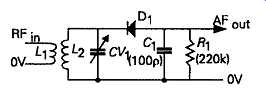
FIG. 2 Simple diode demodulator circuit.
A rather better way of extracting the modulation component from such a rectified carrier signal is to interpose a low-pass filter between the rectifier and the signal output point, as shown in FIG. 3, but even this cannot entirely solve the problem of AM demodulation distortion, particularly at lower carrier, and higher modulation frequencies, so demodulation distortion remains a characteristic of all AM receivers.
The second problem with a demodulator system based on a simple diode rectifier, of the kind shown in FIG. 2, is that low applied voltages may either not cause the diode to conduct at all, or, if a forward bias is deliberately applied, to ensure that they do, or if a semiconductor junction is employed which does have some conduction at zero applied voltage, as shown in FIG. 4, there will be very little difference between the diode forward and reverse direction conduction characteristics for very small input signal voltages.
This leads to a very low demodulation efficiency, a characteristic which it shares with the other 'slope demodulator' circuits shown in FIG. s 5 and 6, which rely for their rectification ability on the curvature of the Vy/C, or Vg//d, characteristics of the semi conductor device.
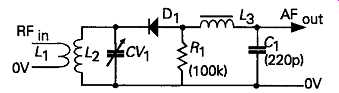
FIG. 3 Improved diode detector circuit
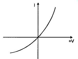
FIG. 4 Conduction characteristics of forward biased diode junction
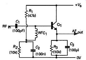
FIG. 5
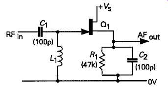
FIG. 6
The so-called 'grid leak' detector circuit, shown for a triode valve in FIG. 7, exploits the fact that as the positive-going peaks of the RF waveform applied to the valve grid approach zero potential, the flow of grid current into C1 will negatively bias the grid of the valve, which will push the mean DC level of the input signal down the/a/Vg slope, as shown in FIG. 8.
This makes the modulation envelope lop-sided so that the average anode current of the valve fluctuates in sympathy with the carrier modulation level. This scheme could also be used with a junction FET, but, in this case, the FET gate would need to be forward biased to the point at which diode type gate conduction was about to occur. Traditionally, the grid leak resistor would be connected across Cl5 to minimize the resistive damping of the input tuned circuit, (L2ICV{), but since Rx would usually be a megohm or greater in value, the damping due to this cause would be negligible, and Rx could equally well be taken to the OV line. This type of demodulator shares with the diode detector the problem of modulation distortion due to the finite R\ICX discharge time constant, as well as the problem that, for small signal levels, the demodulation efficiency is exceedingly poor.
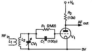
FIG. 7 Valve grid leak demodulator circuit
Clearly, what is needed is some way of increasing the size of the incoming RF signal to a level at which the demodulation efficiency from any of these systems reaches a useful level.
Effect of the Q of the input tuned circuit Some assistance in increasing the magnitude of the applied signal will be given by the action of the Q, (circuit magnification factor) of the input tuned circuit, interposed between the aerial and the demodulator, in FIG. 9, but, to prevent the low input impedance of a demodulator diode, or that of the base/emitter junction of the transistor, from lowering the Q too much, it will be necessary to take the output from the tuned circuit from a low tapping point on the inductor, (L2), which will also lower the available output volt age.
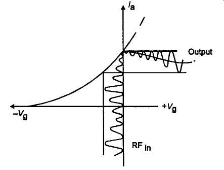
FIG. 8
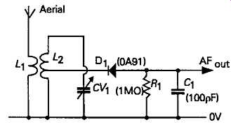
FIG. 9 Simple diode detector radio receiver circuit.
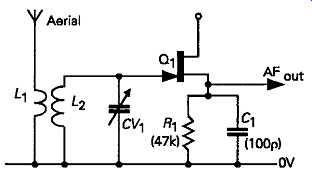
FIG. 10 Radio receiver circuit based on FET slope detector
The FET slope demodulator of FIG. 6 has a very high input impedance, and can therefore be connected across the whole of L2, as shown in FIG. 10, with a significant gain in demodulator output.
The normal engineering solution to this basic problem -- that all AM demodulator circuits require an adequate RF input for satisfactory performance -- is to provide some pre-demodulation RF signal amplification, using the type of circuitry examined in Section 12. Simple receiver layouts of this kind, using one or more tuned RF amplifier stages preceding the demodulator, such as that shown in a contemporary form in the circuit layout of FIG. 11, would be described as a TRF (tuned radio frequency) receiver, and systems of this kind formed the bulk of early radio designs.
FIG. 11 Radio receiver circuit using cascode connected FET RF amplifier
stage.
Problems with selectivity:
There are a number of fundamental difficulties with this approach, of which the major one is that of pro viding adequate selectivity in respect of adjacent frequency signals. As seen in Section 11, a single tuned circuit gives a response curve of the kind shown in FIG. 12, in which the -6dB voltage gain points occur at frequencies separated from the resonant frequency by +l-fJQ. The relative voltage output from a parallel resonant tuned circuit at frequencies on either side of resonance can be calculated, approximately, for values of Q in excess of 10, from the formula given below (Dobbie and Builder, Radio Designers Hand book, fourth edition, pp. 415-416):
... where EJE is the ratio of output voltage at resonance, f_0, to that at a frequency, f, on either side of resonance.
This shows that the -12dB gain points occur at approximately +/-2/0/ß, the -18dB points at+/- 4fJQ9 and the -24dB points at +/-S/JQ. (Note. This type of calculation is only approximate, and shows a symmetrical gain/frequency curve, whereas, in reality, the cut-off characteristic must be somewhat steeper on the lower frequency side of resonance than the higher frequency side.)
Relative transmission (dB)
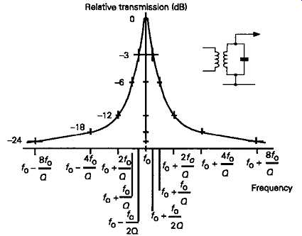
FIG. 12 Response curve of single loosely coupled LC resonant circuit
Using the above data, based on an operating frequency of 200kHz, and a Q value of 100 (a good average value for a well made tuned circuit), the-6dB points would occur at 198kHz and 202kHz -- a 4kHz passband: the -12dB points at 196kHz and 204kHz --an 8kHz passband: and the -18dB points at 192kHz and 208kHz -- a 16kHz passband. If we accept that an 8:1 (18dB), rejection ratio for an adjacent signal is acceptable -- it’s clearly not very good -- the ability of a receiver with a single input tuned circuit, having a Q value of 100, to provide adequate selectivity at a 200kHz operating frequency would require that adjacent stations were not closer than 16kHz in their carrier frequencies. For an operating frequency of 1MHz, these pass-bandwidth figures will be five times as great, and clearly not acceptable for the degree of crowding which exists on any broadcast band.
To improve the selectivity, one must either have more tuned circuits before the demodulator stage, or one must increase the Q of the circuits. Ganged (mechanically coupled) tuning capacitors are available to allow simultaneous tuning of more than one tuned circuit, which will help to solve the problem of selectivity, but while 2-gang tuning capacitors are inexpensive and easy to buy, 3-gang ones are costly and relatively scarce, and 4-gang types are very seldom found, and would be very dear even if they were available, so the number of variable capacitor tuned RF stages which the designer could employ in a TRF type receiver would be mainly limited by the availability of hardware.
Regeneration or reaction:
An ingenious solution to the problem of low Q values, and poor selectivity, which is particularly acute on the 'short wave' bands (approximately 2.5MHz-30MHz), is to use 'regeneration' or 'reaction'. In this technique, some energy is fed back from the output of the amplifying stage into the input circuit, in an identical manner to that employed in an LC type HF oscillator.
However, if the amount of energy fed back is carefully adjusted, so that the circuit does not quite break into oscillation, it’s possible to use the feedback signal to very nearly completely cancel the energy losses in the tuned circuit. With care, and delicate adjustment, operating Q values for the input tuned circuit as high as 50,000 can be obtained by this means. For a receiver operating at 20MHz, this would give a -18dB pass band of 3.2kHz, which would be adequate to separate most wanted signals. This arrangement would also have the great advantage that the incoming aerial signal would also be magnified by the Q factor, so that a 50µF aerial signal would become a 2.5V signal at the demodulator input -- a level at which efficient demodulation would occur.
Because of the simplicity and efficiency of such circuits, designs for one valve short-wave receivers using regeneration, such as that shown in FIG. 13, were very common in the amateur magazines during the 1930s and 1940s. A comparable contemporary design, using two transistors to achieve a similar audio output power, is shown in FIG. 14.
Super-regenerative receiver systems
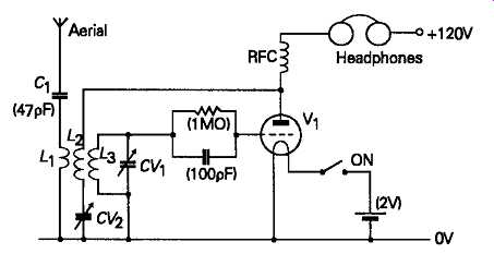
FIG. 13 One-valve receiver regeneration
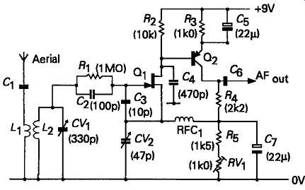
FIG. 14 Simple AM receiver using re-regeneration -- usable over the frequency
range 150kHz-30MHz.
While, with careful adjustment, regeneration provides a very simple and effective method of increasing receiver sensitivity and selectivity, it suffers from the problem that no single setting of the regeneration control will be satisfactory over the whole of the desired tuning range. This is because any alteration in the resonant frequency of the tuned circuit will require an alteration in the L:C ratio in that circuit. But the Q of the circuit is defined by the relationship …so altering the tuning will inevitably alter the Q value of the circuit, and, in consequence, the amount of positive feedback needed to cancel the circuit losses.
This means that the user of the receiver needs to fiddle continuously with his regeneration control knob as he tunes his receiver, to keep on the correct side of the knife-edge between stable operation, and an audible 'howl', which is irritating both to the user and also to others within range of the RF signal inadvertently radiated by his oscillating receiver.
An ingenious solution to this problem, again introduced by Edwin Armstrong, in 1921, is the 'super regenerative' system. This takes advantage of the fact that even when a sufficient amount of positive feed back is applied, around an amplifier stage containing a tuned circuit, to cause it to break into oscillation, there is a finite time lapse between the moment of applying the feedback, and the onset of oscillation.
Armstrong's approach was therefore to apply an external 'quench' signal periodically to the regenerative circuit, to pull its operating point back from the point at which continuous oscillation will occur. This quench signal can be any convenient method of momentarily reducing either the stage gain or the amount of feedback -- even a grid-leak/capacitor combination, whose values have chosen to make the oscillator 'squeg', will work.
However, for simplicity and reliability of operation in a super-regen receiver, the best approach is usually just to superimpose a suitable amplitude sine-wave or square-wave on the HT supply line to the regenerative stage. In order to prevent the whistle due to the quench waveform from blotting out the wanted signal, the quench signal will usually be chosen to be at some ultrasonic frequency, which will facilitate its separation, by simple filtering, from the wanted signal.
Experience has shown that the best receiver sensitivity is obtained with quench frequencies just above the audible range. A simple modification to the re generative receiver circuit shown in FIG. 14, using an externally applied square-wave, of 1-2V amplitude, at 25kHz, to convert it into a super-regen. receiver, is shown in FIG. 15. Any suitable square-wave generator, of the kinds shown in Section 13, will work.
Although super-regen receivers are simple and effective, especially at higher signal frequencies where other receiver systems are less efficient -- and are widely used in 'Citizens Band' (CB) receivers for this reason -- they suffer from several snags which have prevented their more widespread adoption. These are the annoyingly loud inter-station noise (due, it’s said, to randomly occurring thermal noise impulses in the input circuit being amplified by the circuit up to full output voltage level), wide-band noise being radiated from the receiver in the neighborhood of its tuned frequency, and the relatively poor input signal selectivity.
Quench signal:
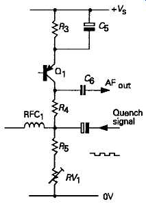
FIG. 15 Modification to convert circuit of FIG. 14 to super-regenerative operation.
Effect of selectivity on the received signal
So far, all our calculations on the ability of a receiver to reject an unwanted adjacent signal have failed to consider the effect of this selectivity on the sidebands of an AM broadcast signal, which are themselves composed of the sum and difference outputs of the modulation and carrier frequencies. Too narrow a reception bandwidth in the receiver will attenuate the higher modulation frequencies, and this is an inevitable effect with any system based on either a single LC parallel resonant tuned circuit, or a series of these connected in cascade to improve the selectivity, simply because the output voltage from such a tuned circuit will fall immediately the signal frequency moves away from the frequency of resonance.
Tuning successive stages, in a cascaded series of tuned circuits, to slightly different frequencies will increase the receiver bandwidth, but this is a difficult practice to carry out well. A much better approach, which is very widely employed, is to use pairs of tuned circuits which are electrically coupled to one another, as shown, for example, in the inductively coupled layout of FIG. 16.
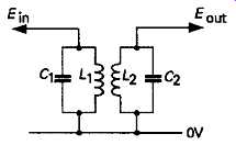
FIG. 16 Bandpass-coupled pair of tuned circuits
Bandpass coupled tuned circuits:
Such bandpass-coupled pairs of resonant LC circuits, of which a number of possible layouts were shown in Section 11, have the great advantage that, for appropriate values of Q and coupling factor, the pass-band has a portion, adjacent to the resonant frequency, at which the signal output will be substantially constant, as shown for a critically coupled bandpass system in FIG. 17. Circuits of this kind can be cascaded, to improve the steepness of the skirt frequency response, without impairing the flatness of the portion of the response curve on either side of resonance, and this level response portion can be tailored, by choice of Q and coupling factor, to provide almost any desired pass-band.
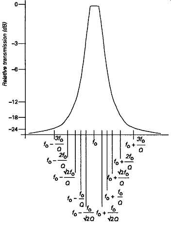
FIG. 17 Frequency response curve of critically coupled bandpass pair of tuned
circuits.
However, these factors will depend on the operating frequency chosen, and this factor, quite apart from the impossibility of obtaining 4-, 6-, or 8-gang tuning capacitors, precludes the use of bandpass-coupled RF stages in simple TRF receivers, and has led to the almost universal adoption of the 'superhet' system.
The supersonic heterodyne, or superhet system As with so many other useful ideas in the field of radio, this was introduced by Armstrong, in 1921, and pro vides an effective solution to the problem of selectivity, while avoiding the difficulty of trying simultaneously to tune a number of critically coupled bandpass-coupled circuits. The basic idea of the superhet receiver is illustrated in FIG. 18. In this arrangement, the incoming signal is converted, in a frequency changer or mixer stage, into a signal at some other fixed, intermediate, frequency at which the bulk of the pre-demodulator, RF, amplification is per formed. This frequency conversion is carried out by combining the incoming signal with the output of a local oscillator in a stage having a sufficient degree of nonlinearity as an amplifier to cause the generation of sum and difference products as a result of the interaction between the input signals. By the choice of a suitable local oscillator frequency, a composite output signal, carrying all the modulation information present on the incoming aerial signal, can be generated, and can be placed at any desired frequency. This allows the intermediate frequency to be chosen to lie at any convenient part of the RF spectrum.
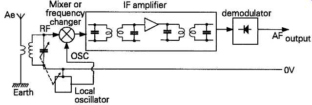
FIG. 18 Basic layout of superhet receiver ---Mixer or frequency changer;
RF IF amplifier demodulator AF output; Local; oscillator.
For example, for an incoming signal frequency of 1550kHz, and a local oscillator frequency of 1000kHz, sum and difference frequencies of 550kHz and 2550kHz will be generated, and will be present in the mixer stage output, along with the original 1550 and 1000kHz input frequencies.
For low to medium frequency receivers, such as are widely used for the medium- and long-wave broadcast bands, the IF frequency normally chosen is 455 or 465kHz, and this frequency band is kept free of most commercial broadcast transmissions. For earlier de signs of short-wave receivers, 1.6MHz, a frequency right at the upper end of the medium-wave band, and not, at that time commercially exploited, was commonly chosen as an IF frequency, but in more modem designs, 45MHz or even higher frequencies may be used. Since it’s desirable to avoid direct aerial circuit break-through at the chosen intermediate frequency, the frequencies adopted for IFs are usually those free from existing broadcast signals. It’s also normal practice, because it facilitates mixer stage design, to adopt the Oscillator high' style of operation, in which a receiver with a 455kHz IF amplifier stage, covering the frequency range 650kHz-1600kHz, would employ a local oscillator tunable over the range 1105kHz-2055kHz (i.e. above, rather than below, the received signal frequency). The use of a fixed frequency IF amplifier conveys an enormous advantage in receiver design, in that almost any desired amount of amplification can be provided, and the adjacent channel selectivity can be chosen to give any required cut-off characteristic and passband, whether by the use of a cascaded series of bandpass-coupled, or stagger tuned, circuits, or by the use of a quartz crystal, mechanical resonator, or ladder filter, or some other surface acoustic wave type of RF passband defining system.
There are, however, also some drawbacks with the superhet system, of which the chief ones are 'second channel' reception, mixer noise, drift of the tuned frequency, poor mixer conversion efficiency, whistles and cross-modulation effects.
Second-channel interference:
Second-channel or image frequency reception can al ways occur in a frequency changer, for the reason which can be illustrated using the case of the receiver described above. For example, if the local oscillator is tuned to 1105kHz to produce a 455kHz IF output from a wanted 650kHz incoming signal, it will also produce a 455kHz output with an unwanted 1560kHz incoming signal, if one should, by chance, be present. The only way by which this can be prevented is by making sure that the selectivity in the RF amplification, or other tuned frequency, stages between the aerial and the mixer input is adequate to reject the unwanted image frequency signal. For signal frequencies up to a few MHz, the task of providing adequate RF selectivity to reject an unwanted signal 910kHz away from the wanted signal frequency is quite easy to accomplish.
However, for a signal frequency of, say, 20MHz, an adequate degree of rejection of an unwanted second channel signal at 20.910MHz will be much more difficult to secure. This was the reason for the choice of a 1.6MHz IF in early short-wave superhets: that the image frequency would be 3.2MHz away from the frequency of the wanted signal, and therefore some what easier to reject.
Double superhets and direct conversion systems Since the efficiency of an IF gain stage will decrease as the operating frequency is increased, the 1.6MHz IF signal might then be down-converted to 455kHz for further amplification and pass-band filtering, as shown in the schematic layout of FIG. 19. This process is termed 'double conversion', and such a receiver is called a 'double superhet' to distinguish it from the 'single conversion' method used in the simpler design of superhet receiver.
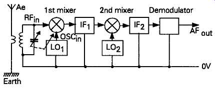
FIG. 19 Layout of double superhet. 1st mixer; 2nd mixer; Demodulator; Earth.
The process may be extended yet further, for example to a 'triple conversion' receiver, with three IF gain blocks, and three successive frequency changer stages. In the opposite direction of development, there are what are termed 'direct conversion' receivers, shown in FIG. 20, in which the incoming signal is mixed with a locally generated one, usually derived from a crystal controlled oscillator, operating at, or near, the same frequency as the wanted signal.
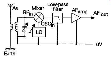
FIG. 20 Direct conversion receiver.
In the case of a transmitter whose carrier is keyed to send a Morse coded message, the output from the mixer could then be an interrupted audible difference frequency tone. In the case of a single-sideband sup pressed-carrier transmission, provided that the oscillator frequency was chosen correctly, the output from a direct conversion receiver could be a normal audio band speech signal, without the need for any additional demodulator.
For a double-sideband transmission, with carrier, there would be an audibly objectionable 'howl' if the locally generated oscillator signal in a direct conversion receiver differed in frequency from the received carrier by an amount which was within the audible pass-band, and this limits the usefulness of such a system. Nevertheless, there are double-sideband receivers, in which synchronous frequency local oscillators are employed. These are called 'homodyne' or 'synchrodyne' systems, and are discussed later.
Whistles and mixer noise:
A further problem with all superhets is the presence of whistles, which may occur anywhere within the tuning band. These are usually due to the presence at the input to the mixer stage of harmonics of the intermediate frequency signal -- mainly generated at the demodulator stage -- which then interact with incoming RF signals. Alternatively, oscillator harmonics can pro duce whistle generating IF frequency signals by mixing with signal harmonics.
In principle, a superhet will always have a somewhat lower signal-to-noise ratio than a simple TRF receiver, because of the additional noise introduced by the mixer stage. This noise occurs for exactly the same reasons as the thermal noise which is found in any other high gain amplifier system, and is a function of the effective conversion bandwidth, the effective input impedance of the system, and the ambient tempera ture. The problem is worsened by the relatively low stage gain (conversion efficiency), of the mixer stage, which means that its output noise level -- bearing in mind that its output impedance may be fairly high --may be amplified nearly as much as the desired input signal.
Frequency drift:
Another difficulty peculiar to the superhet is that of oscillator frequency drift, which causes a corresponding drift in the tuned frequency of the receiver. This problem is mainly caused by changes in the ambient temperature of the oscillator capacitors and inductors, and methods for minimizing this are discussed later.
However, frequency drift can also be caused by changes in the input impedance of the oscillator or mixer devices, as well as by component ageing effects, or by the effects of mechanical vibration or external capacitative or inductive fields.
In VHF receivers, where high frequency IF stages, such as 45MHz, are used to reduce image frequency signal intrusion, the instability of tuning, with even a well designed variable frequency LC oscillator, would be quite unacceptable, and this problem is worsened because such receivers will inevitably require that the local oscillator operates at a frequency placed above the desired signal frequency. Practical receivers of this kind must therefore either use drift cancelling circuit techniques, or frequency synthesizer systems, based on a stable frequency quartz crystal reference oscillator. These techniques are explored later in this section.
A further associated problem is that of local oscillator frequency pulling, because of the effect of the aerial input signal on the impedance which the mixer stage presents to the local oscillator. This can largely be eliminated by good design procedures, such as the inclusion of a buffer amplifier between the oscillator output and the mixer input.
Cross-modulation:
Two other associated difficulties are those of inter modulation and cross-modulation within the mixer stage. The first of these effects is due to harmonics of input signals, produced by the essential nonlinearity of the mixer, creating spurious higher frequency signal images. The second, again due to mixer nonlinearity, is the more annoying problem in which a strong in coming signal, by causing the mixer input working point to move up and down its transfer characteristic, will add its own program modulation to that of the wanted signal.
Avoidance of these faults requires care in mixer stage design, and some limitation of the size of the signal level at the mixer input. For this reason, pre mixer RF gain is usually chosen to be high enough to ensure that the overall signal-to-noise ratio of the receiver is mainly due to the aerial input circuit, but not so high that inter- and cross-modulation effects become noticeable.
Practical mixer circuitry:
In thermionic valve operated equipment the most common frequency changer stages are the triode hexode, or heptode, valve types illustrated in FIG. 21.
These are, essentially, screened grid or RF pentode valves in which the screening grid has been separated into two sections, with an additional control grid inserted between them. This grid is internally connected to the control grid of a triode, which is contained within the same envelope and which shares the same cathode as the hexode/heptode. The internal triode section can then be employed as a separate RF oscillator whose output will modulate the electron stream flowing through the hexode/heptode section. This gives the required sum and difference signal generation, but screens the oscillator signal from the aerial input circuitry to avoid unwanted radiation of the local oscillator RF output. Unfortunately, although the triode- hexode/heptode mixer valve can give a good IM and cross- modulation performance -- if the circuit operating conditions are chosen correctly -- it has, by modern standards, a relatively poor noise figure.
In low-cost portable transistor radio receivers, where the principle requirement of the manufacturer is to keep the total component count as low as possible, earlier circuit designs usually employed a self-oscillating mixer, of the general type shown in FIG. 22, using a bipolar junction transistor, in spite of the fact that this type of circuit can only give a relatively poor performance in technical terms.
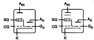
FIG. 21 Triode-hexode and triode-heptode frequency changer valves
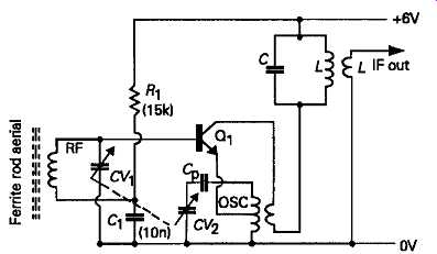
FIG. 22 Circuit layout of single transistor frequency changer
In contemporary low-cost design practice the preferred approach is to use a single integrated circuit, such as the LM1868, in which all the functions of mixer, IF amplifier, demodulator, automatic gain control, and probably also those of a low power AF output stage, are fabricated on a single chip. Although the IC designers are forced to choose circuit configurations which minimize the use of hard-to-make capacitors and resistors, and this constraint can lead to some odd-looking circuit layouts, the basic electronic structures used in this type of IC will generally be similar to the circuit configurations used with discrete component designs. So such ICs, although effective in keeping the manufacturers component count down to a low level, will still usually only offer a comparably indifferent technical performance. Such single chip IC radio systems will usually also incorporate an FM receiver section: a method of signal transmission which is examined later in this section.
The best practicable performance for a multiplicative mixer (one in which the output signal is the product of the aerial and local oscillator signals) is given by a system in which there is a 'square-law' relationship between the input voltage and the output (anode, collector or drain), current of the mixer device, and this condition is met most nearly by a junction FET operated at or near zero gate bias.
An efficient, low-noise, mixer circuit is provided by the circuit shown in FIG. 23, where the aerial signal is applied to the gate and the local oscillator signal is injected into the source circuit of a junction FET, though this does not give a very good isolation of the oscillator signal from the aerial circuitry, unless an RF or other buffer stage is interposed between the aerial and the mixer. The relatively limited optimum working voltage range of such a circuit also limits the range of signal voltages which can be handled without input overload.
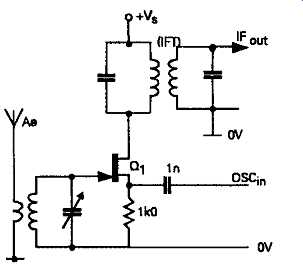
FIG. 23 FET mixer layout.
This circuit can be elaborated using the cascode layout of FIG. 24, which gives a somewhat better degree of input/output/oscillator circuit isolation.
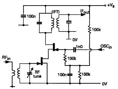
FIG. 24 Cascode connected FET mixer system
These advantages are shared by the dual-gate MOS FET circuit shown in FIG. 25, a layout which is very commonly used in medium quality discrete component superhet systems. The Id/Vg characteristics of the dual-gate MOSFET are not quite as favorable from the point of view of avoidance of cross-modulation as those of the junction FET, though some MOS FETs are designed specifically for mixer applications, where the gate characteristics have been modified to suit this application. MOSFETs don’t generally have such a low noise figure as junction FETs. They may, however, have better input overload behavior.
