AMAZON multi-meters discounts AMAZON oscilloscope discounts
OVERVIEW
As digital system frequencies increase it will become increasingly difficult to minimize electromagnetic radiation from the system. This creates a developing problem for the digital system designer in designing products that will pass the Federal Communication Commission's, or other regulating agency's, emission standards, commonly known as the EMI (electromagnetic interference) specifications. The importance of passing EMI specifications often takes precedence over many other design or functional requirements of a product because unlike other requirements, the need to pass EMI criteria is rooted in a government-driven specification rather than inspired by a market demand or engineering principles. In fact, it is, unfortunately, quite common, for system designers to be forced to compromise their own system timing requirements in order to pass the EMI test and be allowed to sell a product.
The topic of EMI is particularly difficult to handle in an engineering context because there are usually far too many variables to handle quantitatively and the EMI solution can usually not be finalized until prototypes have already been built and measured for compliance and failure mechanisms. At this late stage of the design cycle, it is often very difficult and expensive to make changes. This often leads to desperate measures, cost and schedule overruns, or solutions that compromise the intended function of the product.
Numerical or closed-form predictions of radiated emissions tend to be limited in utility, and expert systems are useful only for very limited purposes and are also inherently flawed by the inability to provide the program with enough input. Although many efforts are under way to develop more useful tools, the tools of the day do not do much better in predicting or suggesting solutions than an EMI specialist does "eyeballing" the system. It is encouraging for system designers, however, that the EMI engineer's specialized knowledge tends to be mainly composed of a few basic principles, some general design rules, an ability to apply trial and error, and a capacity to know when to abandon a theory or a rule of thumb. The design engineer's knowledge of these principles can prevent a late-blooming catastrophe.
One can begin to realize the difficulty in making accurate quantitative predictions by considering the fact that even the simplest antenna shapes are very difficult to solve and usually are solved only by relying on assumptions or empirical measurement. It is no surprise, then, that in systems with thousands of traces, complex shapes, many cables, and other variables, the subject some-times tends to fall closer to superstition and mumbo jumbo than do most topics in engineering. It is very frustrating to rely on best-known methods that may not work, particularly when the reasoning behind them (or lack thereof) is not evident to the designer. The intent of this Section is to equip the reader with the basic understanding and practical skill necessary to best navigate the task of minimizing radiation in all stages of a design cycle from conception to product.
1. FCC RADIATED EMISSION SPECIFICATIONS
Several regulatory agencies exist around the world which concern themselves with electromagnetic compatibility (EMC). In the United States, the Federal Communications Commission (FCC) sets forth EMC standards. Among these EMC standards are both conducted emission (such as noise conducted back through the power grid) and radiated emission limits. This Section is concerned primarily with radiated emissions since that is typically the dominant emission problem in high-speed digital design.
The FCC radiated emission limits for digital devices is shown in Appendix F. There are two types of digital devices, class A and class B, each with its own emission requirements. Class B devices are those that are marketed for use in a residential environment, and class A devices are those that are marketed for use in a commercial, industrial, or business environment. Note in Appendix F that the class A and class B emission requirements are specified at different measurement distances. There is one more requirement, the open-box emission requirement, pertaining to computer motherboards that are marketed as a component rather than inside a complete system with a chassis. The open-box emission requirement is an emission requirement that must be passed with the chassis cover removed. The open-box requirements are relaxed from the closed-box requirements by 6 dB. This means that if a motherboard is to be marketed as a component rather then included in a complete system, under current regulation no more then 6 dB should be anticipated from chassis shielding.
2. PHYSICAL MECHANISMS OF RADIATION
One can show from classical electromagnetic theory that any accelerated charge radiates.
Thus, in a digital system, which must accelerate charge in order to create electrical signals, radiation is inevitable. However, the rest is not that simple. It is well known that even very simple antenna shapes are difficult to analyze. Even the case of geometrically perfect shapes and perfect conductors, such as the case of a straight wire excited in the middle (half-wave dipole antenna), has been the subject of research for many years and is solved only by making assumptions about the current distribution. Thus in a real system with complex shapes, a myriad of impedance paths, many frequency components, and many unknown, unpredictable, or non-measurable variables, one may easily imagine that the task of predicting, controlling, and diagnosing radiating emissions would be intractable. To complicate matters, borrowing from methods that worked in the past could lead to more difficulties, because rule-of-thumb design practices are particularly treacherous if the user does not know in the appropriate situations to apply them. This is because several techniques contradict each other, and often to fix one mode of radiation, you cause another mode to increase.
Straightforward accurate simulation of the radiated fields generated from a complex system is generally not feasible, and even when done, is only sufficient to augment the judgment of a human engineer. This reveals the encouraging fact that application of a few simple principles can significantly reduce the complexity of the problem.
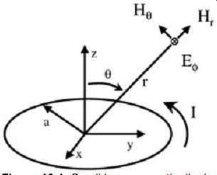
FIG. 1: Small loop magnetic dipole.
2.1. Differential-Mode Radiation
Differential-mode radiation results from current flowing in a loop. The model for differential mode radiation is usually based in equations derived for a small magnetic dipole where the circumference, or the length, of the loop is much smaller than the wavelength (wavelength = _ = c/F, where c is the speed of light) of the signal (i.e., 2pa = l << _, such as shown in FIG. 1). The application of this to a larger loop, encountered frequently in real-life systems, will be explained later. The following equations are from the solutions of Maxwell's equations derived for an ideal magnetic dipole and are modified here to show only the field magnitude:
(1a)
(1b)
(1c)
…where…
E_ = magnitude of the electric field, in volts per meter H? = magnitude of the ? component of the magnetic field, in amperes per meter Hr = magnitude of the r component of the magnetic field, in amperes per meter
?0 = 120p = 377 ohm = intrinsic impedance of free space
_ = wavelength, in meters I = current, in amperes A = area of the loop, in square meters r = distance from the center of the loop (see FIG. 1)
---= angle from z-axis (see FIG. 1)
Similar solutions can be found in a multitude of electromagnetic textbooks for the interested reader. They are stated here to understand the basis of the practical approximations that will follow.
Notice that ? = p/2 produces the worst-case field strength of E_ and H?. Also notice that Hr falls off very rapidly with distance r from the center of the loop. The worst-case angle of ? = p/2 will be assumed and Hr will be considered negligible for all that follows.
Differential Mode Near-Field Radiation.
In conditions where the distance r < _/2p, known as the near-field, terms with large exponents are dominant and the formulas reduce to…
(2a)
(2b)
…where…
Edm near = differential mode near-field electric field strength, in volts per meter Hdm near = differential mode near-field magnetic field strength, in amperes per meter
?0 = 120p = 377 ohm intrinsic impedance of free space
µ0 = permeability of free space = 4p × 10^-7
H/m I = current, in amperes A = area of the loop, in square meters
_ = wavelength, in meters F = frequency, in hertz r = distance from the center of the loop, in meters
Note that both the magnetic and electric components are strongly dependent on distance and the magnetic field is independent of frequency.
For future discussion, let us define the wave impedance to be the ratio E/H. The wave impedance for the near field of a loop radiator can be derived from (2a) and (2b) and is (3)
The wave impedance affects how strongly the wave will couple to other structures of given impedances, as discussed later in the Section.
One may expect that the impedance of the wave in the vicinity of the circuit should be related to the circuit impedance, because, in fact, the circuit impedance itself is a result of the local fields (such as in , seen in other Sections as the impedance of a transmission line). With this in mind, examining equation (3) reveals that the impedance is low when _ is large. This approaches the dc impedance of the perfectly conducting uniform current loop in the model. Much like a perfectly conducting inductor, the impedance goes up in direct proportion to frequency (inverse proportion to wavelength).
Differential Mode Far-Field Radiation.
If distances r > _/2p, are considered, the terms with the large exponents will be negligible and the formulas will reduce to (4a) and (4b). The conditions where r > _/2p is known as the far field.
(4a)
(4b)
Similar to before, the wave impedance can be calculated from the ratio of (4a) and (4b). The result is not surprising: Zdm wave far = ?0 = 120p, which is the intrinsic impedance of free space.
Calculation for Nonideal Loops.
Many references directly apply the equations derived above for applications that violate the initial assumption of l << _ (loop length must be small compared to the wavelength). The reader should be aware that the ideal loop equations derived here are no longer theoretically correct when the condition of l << _ is not met. At lengths larger than this, the circuit path will begin to behave like transmission lines and the current will no longer be uniform. For greater accuracy using the equations derived above assuming an ideal loop, the length of the loop should be less then approximately _/10. However, for the purposes here, the equations can continue to be used for longer lengths if the following approximations are made. For total circuit loop lengths l = _/2, the length l should be clamped at l = _/2 and the area A input into the equations above should be adjusted accordingly. For lengths l < _/2, the actual loop area is used. For example, if the path is circular and the loop length is greater than _/2, the corrected area A to be entered in the equations above should be calculated with a radius that produces a circumference of _/2 [C = _/2 = 2pr ? r = _/4p, thus A = p(_/4p) 2 ]. If the path is a square rectangular loop, the corrected area A should be (_/8) 2 = _2/64 (since the total loop length is _/8 + _/8 + _/8 + _/8 = _/2). The physical reason for this "antenna shrinking" effect is that if the antenna is long enough compared to the frequency such that different peaks and valleys of the waveform exist on the antenna simultaneously, the various peaks and values will cancel each other's radiation.
APPLICATION RULE
If the total loop path l is longer than _/2, the area A input into loop equations should be adjusted to the area that would be present with a maximum path of l = _/2.
As the reader may recall from equation (3), the near-field wave impedance was related to the circuit impedance assuming that the dc impedance was zero (perfectly conducting), which is not realistic. For the practical case, such as circuit loop that contains a source and load impedance (such as shown in FIG. 2), the ideal assumption breaks down. The following equation calculates the near field for the nonideal case (when the total circuit impedance of the loop Zc = Zs + ZL = 7.9 rF × 10-6 ).
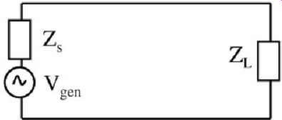
FIG. 2: Nonideal loop that contains impedances. (5)
Equation (2a) is valid if the impedance is less then 7.9 rF × 10-6 ohm. Furthermore, the modification is not required for the far field regardless of total loop circuit impedance. Note that the equation is written in terms of voltage instead of current. The other differential-mode equations may be written for voltage by approximating I = V/Zc. Some practical applications of (2), (3), (4), and (5) are explored later in the Section.
Problematic Frequencies.
Let us make a general approximation of which frequencies are of most concern in a digital system for differential-mode radiation. Consider FIG. 3, which shows a Fourier spectrum of a trapezoidal clock signal and the associated envelope that typically bounds the spectrum of a digital signal. For a perfectly symmetric (i.e., 50% duty cycle) digital signal, one can verify with Fourier analysis, no even harmonics will be present in the system.
However, in reality there are sometimes significant even harmonics.
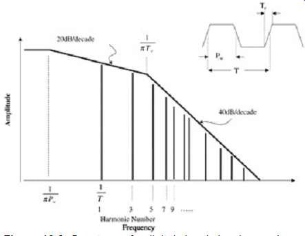
FIG. 3: Spectrum of a digital signal showing peak envelope regions.
Note that the frequency envelope of the Fourier spectrum shown in FIG. 3 falls off with frequency at a rate of -20 dB per decade (an inverse linear relationship with frequency) up to f = 1/pTr after which it falls off at a rate of -40 dB per decade (an inverse-square relationship). Now consider the far-field radiation [equation (4a)], which is directly proportional to the square of frequency and thus increases with frequency at a rate of +40 dB per decade.
However, when the loop path is greater then _/2, the effective loop area is adjusted to be a constant times _2 (the constant will depend on the area calculation of the shape of the loop). Thus at high enough frequency, the _2 component of the area A in equation (4a) will cancel with the _2 element, and the field will stay constant with increasing frequency. This will happen at a frequency F = c/2l (where c is the speed of light and l is the loop length). FIG. 4 shows the relative radiated magnitudes of different frequencies input into a given loop. Note that the loop will radiate frequencies with increasing efficiency up until the antenna shrinking effect occurs at frequencies above F = c/2l.
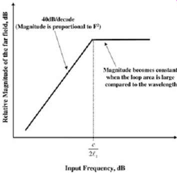
FIG. 4: Relative magnitude of far-field radiation as a function of frequency.
When the spectral envelope of the digital signal (the input into the radiator) is combined with the frequency dependence of the far-field radiation shown in FIG. 4, we arrive at the differential radiated emission envelope shown in FIG. 5. Note that the frequency F = 1/pTr will not necessarily occur at a higher frequency than F = c/2l, as shown in the figure.
The frequencies that will be most likely to radiate (differential mode) are contained between the frequencies F = 1/pPW and F = 1/pTr or F = c/2l (whichever is highest).
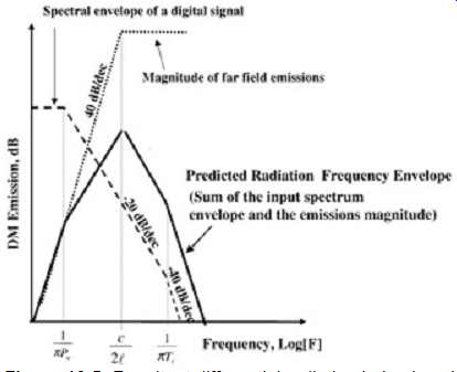
FIG. 5: Resultant differential radiation behavior when far-field characteristics
are combined with spectral input.
RULE OF THUMB: Minimizing Differential-Mode Radiation
Since the magnitudes of the fields are proportional to the loop area, smaller loops produce less radiated emission. During design, minimize current loops whenever possible.
2.2. Common-Mode Radiation
Common-mode currents are those flowing in the same direction. A common source of common-mode currents in a digital system is from noise on ground or power planes due to the switching noise of digital circuits. Common-mode currents are likely to cause emission concerns when they find access to external cables, which can act as long antennas. Often, the common-mode effects determine the overall emission performance.
One may attempt to avoid common-mode current altogether by providing return paths for all signals (such as the shield on a cable or by providing a very good ground return path for a signal), in which case one might expect common-mode current to cancel. However, there are always unanticipated return paths that cause some of the return current to deviate from the intended path. This will cause enough asymmetry to cause a net common-mode effect.
FIG. 6 illustrates a simple example of the generation of common-mode current. It takes only a very small amount of current deviating from the expected complete loop to cause significant common-mode emissions.
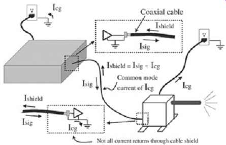
FIG. 6: Common-mode current generation.
The following solutions of Maxwell's equations for an ideal electric dipole are stated here to provide an understanding of common-mode radiation:
(6a)
(6b)
(6c)
…where l is the length of the radiating wire. An electric dipole is illustrated in FIG. 7. An electric dipole is essentially equivalent to an isolated wire in space with the condition that l << _. The bulbs at the ends of the line shown in FIG. 7 are included so that a uniform current can be assumed on the small length of the conductor, due to the capacitance of the bulbs. The interested reader can find similar solutions to an elemental electric dipole in many electromagnetic textbooks. As before, these equations have been modified to show only field magnitude.
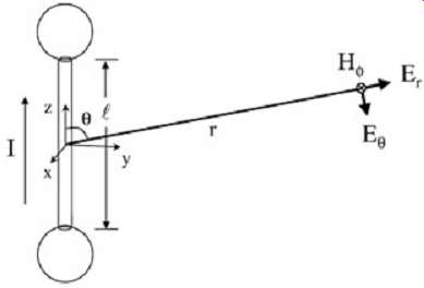
FIG. 7: Illustration of an electric dipole.
Notice that (6b) and (6c) are maximum for ? = p/2. As before, this condition will be assumed from now on for worst-case field emissions. Er falls off more rapidly with distance (inverse r 2 ) from the wire and is neglected in the following approximations.
Common-Mode Near-Field Radiation.
For distances r less then _/2p, the terms with the higher exponents will be dominant, so equations (6b) and (6c) reduce to
(7a)
(7b)
As before, this region is known as the near field. Note that the peak H field is independent of frequency. This equation, in fact, holds down to dc. As before, we can produce the common mode near-field wave impedance as the ratio of (7a) and (7b). E/H is shown in the equation
(8)
As before, the wave impedance close to the radiator can be expected to relate to the circuit impedance. Note that for _ = 8, the impedance is infinite, as one would expect for an open circuited wire.
Common-Mode Far-Field Radiation.
When distances r greater then _/2p are considered, equations (6b) and (6c) reduce to
(9a)
(9b)
This region is known as the far field. Not surprisingly, the wave impedance in this region can be seen [from the ratio of equations (9a) and (9b)] to be the impedance of free space, ?0.
Nonideal Dipole Radiators.
As for the radiating loop, many references directly apply electric dipole equations for frequencies and circuit dimensions that violate the initial assumption of l << _. The reader should be aware that the solutions are not theoretically correct when this assumption is not met. However, equations (7a) and (9a) can be modified to be usable with longer dimensions, much like the length of the loop was modified for the loop radiator, by fixing the length of the radiating wire to _/2. Beyond this length, the radiating wire looks like a transmission line and the current is not uniform. Thus the effective radiating area shrinks.
The fields from the other _/2 segments cancel each other out. If only one side of the radiating wire has a strong capacitance or connection to ground, the radiating wire will behave like a monopole rather then a dipole, and twice the length should be used in equation (9a). It should be noted that at resonant lengths (such as multiples of _/2) where standing waves will be present on the radiator, there will be directional lobes to the radiation, and the maximum field intensity may be significantly higher.
Common-Mode Radiation in the Presence of a Reference Plane.
Another modification is required for a radiating wire if the radiating wire is close to a reference plane (ac ground). A ground plane that extends sufficiently in the vicinity of the radiator (i.e., a quasi-infinite plane) will act as a reflector. The reflected wave will be inverted from the incident wave much like a wave on a transmission line reflecting from a short-circuit termination. Depending on the distance of the reflector and the wavelength being considered, the reflected wave can add constructively or destructively with the radiated wave.
To see the destructive and constructive effects of the reflecting plane, one may use trigonometric identities as follows. Consider the radiated wave to be sin ? and the phase shift angle of the reflected wave to be s = 2p_/h, where h is the distance from the constant voltage plane. Thus the resultant wave will be sin? - sin(? + s). Substituting the trigonometric identity sin(? + s) = sin? coss + cos? sins reveals that if the phase shift is small, such as in the case of a PCB trace over a ground plane, then sins ˜ 0, coss ˜ 1, and the incident wave will cancel with the reflected wave, causing very little radiation. This is why PCB board traces are typically not considered for common-mode radiation except for very high frequencies or traces with no local reference plane. In such a case, the loop radiator equation can still be applied to the board trace. In a case where the phase shift of the reflected wave is larger, say close to a value of p, then sins ˜ 0, coss = -1, and the reflected and radiated waves add constructively to double the radiated amplitude.
For a close ground plane (closer then _/10), the reduction in radiation is sometimes given as…
(10)
…where h is the distance from the reference plane. Factoring equation (10) with equation (9a) …yields…
(11)
Notice that this is very similar to the loop radiation equation (4a).
Problematic Frequencies.
As before, let us determine the emission envelope of most concern. Equation (9a) is directly proportional to F and thus will increase with F at a rate of 20 dB/decade. Recalling the digital spectrum envelope as shown in FIG. 3, and recalling the long wire modification, the envelope shown in FIG. 8 can be constructed in a manner similar to FIG. 5. Subsequently, the frequencies that will be most likely to radiate significantly are contained between the frequencies F = 1/pPW and F = 1/pTr or F = c/2l (whichever is highest).
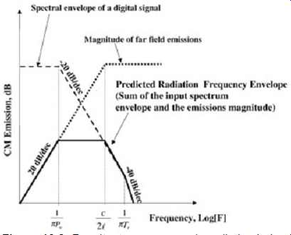
FIG. 8: Resultant common-mode radiation behavior when far-field characteristics
are combined with spectral input.
2.3. Wave Impedance
The wave impedance, the ratio E/H, was mentioned above for each type of radiation. The wave impedance can be thought of as an impedance just like the impedance of a transmission line. Thus, whether the radiated wave will couple to other mechanisms can be understood based on the impedance of the structures. For instance, a low-impedance wave, such as the near-field portion of a loop radiator, will couple to a conductive (low-impedance) shield. A high-impedance wave, such as the near field of a common-mode radiator will be reflected from a conductive shield due to the impedance mismatch between the high impedance wave and the low-impedance shield. For all types of radiation, the far-field wave impedance eventually approaches the impedance of free space, ?0 = 377 ?. The wave impedance is shown graphically in FIG. 9.
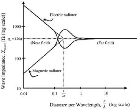
FIG. 9: Wave impedance behavior.
Because emission requirements are typically specified in terms of electric field, there are also dependencies on the measured distance (since a low-impedance radiator in the near field will look magnetic and not show up on the electric field probes). A common practice is to take measurements at a given distance and back-calculate to the distance specified for the emission requirement. This could lead to inaccuracies, depending on the wave impedance.
Understanding the nature of wave impedance can also be a useful diagnostic. For example, if the magnitude of the electric field appears to get larger with increasing distance, then the radiator is probably a loop. To understand this, refer to FIG. 9. Notice that in the far field, the impedance for the electric and the magnetic radiator both assume the value of 377 ohm. This means that the electric field probes used to measure the far-field radiation cannot distinguish between a magnetic and an electric radiator. However, as the probe is moved towards the radiator and into the near field, the measured electric field will decrease with distance for a loop radiator because the radiation becomes primarily magnetic as the wave impedance decreases. Obviously, the opposite also holds. If the magnitude of the electric field increases as the probe is moved towards the radiator, then the radiator is probably due to common-mode currents. Alternatively, if the measured radiation from a problematic frequency in the far field is relatively unaffected by placing a low impedance metal shield in the near field (such as a computer chassis), then this is a clue that the radiator is a loop. If the shielding significantly reduces the magnitude of the radiation, the radiator is probably due to common-mode currents.
3. DECOUPLING AND CHOKING
This section may well extend far beyond the motives of this Section. The simple task of decoupling a high-frequency digital circuit is paramount to signal integrity, power delivery, and minimization of emissions. Decoupling amounts to creating low ac impedance between power and ground structures (although in some circumstances, the exact opposite is done to minimize emissions, this having a negative effect on signal integrity and timings). The importance of decoupling in reducing emissions can be seen from FIG. 10. In the figure it can be seen that the presence of the decoupling capacitor prevents the current from taking a much larger loop path or from finding its way to a cable and radiating as a common-mode radiator. FIG. 10 suggests not only that the local decoupling capacitor value should be chosen appropriately but that the capacitor is placed physically close to the component to minimize the loop area. If current cannot be decoupled appropriately, inductive choking may be used to block the passage of high-frequency noise. Inductive components are regularly used at cable connections to minimize common-mode currents. Occasionally, regions of the reference planes are isolated and choked off with an inductor, as shown in FIG. 11.
Cutting the reference planes should generally be avoided in high-frequency digital systems unless other methods have been exhausted, for reasons explained in this section.
Understanding decoupling or choking is not sufficient without an understanding of a few limitations, particularly at high frequency. Several modifications of the examples presented here exist and are almost universally applicable.
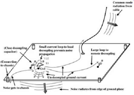
FIG. 10: How proper decoupling minimizes current loops.
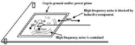
FIG. 11: How inductive choking minimizes current loops.
3.1. High-Frequency Decoupling at the System Level
The model for a real-life capacitor is shown in FIG. 12. Some impedance curves of typical capacitors in typical packages are shown in FIG. 13. Note that each capacitor has a resonance at which its impedance is at a minimum. The effective resonance that forms the minimum impedance point when placed on a circuit board will be slightly different due to the added inductance in the path routed to the capacitor. Note also that the choice of capacitor dielectric can lower the impedance of a capacitor.
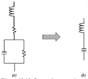
FIG. 12: Decoupling capacitor: (a) real model; (b) model used here.
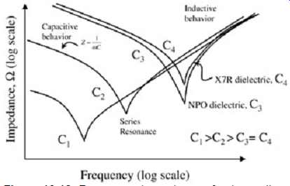
FIG. 13: Frequency dependence of a decoupling capacitor.
The idea behind decoupling is, of course, to provide a minimum ac impedance between power and ground. Thus one may conclude by a glance at FIG. 13 that a few higher value capacitors chosen for low impedance at low frequency paired with some lower-valued capacitors chosen to provide low impedance at high frequencies (near their resonance points) would be the method of choice. This is more or less the optimal way to decouple a board; however, there are other effects that are not immediately obvious. For example, resonance conditions can exist such that the decoupling capacitors can actually worsen the impedance of the power delivery for some frequencies. This can happen when the total inductance associated with the capacitors combines in parallel and resonates with the plane capacitance. This can actually cause the impedance between power and ground to increase to beyond what the impedance would be with no decoupling capacitors present. To see this, let us a build up a model of a decoupled power and ground plane.
Because the inductance of a power or ground plane is very small, let us assume it to be zero.
This allows us to model the power and ground plane structure as a capacitor with no series inductance. Typically, the plane capacitance is on the order of 100 pF/in2 and ground planes (10 mils). These close planes are typically only implemented on boards that have more than four layers, and probably at least eight layers. We will see shortly some benefits of having close planes. It should be mentioned that spacing the planes very close together (i.e., closer then 4 mils) may be a reliability issue with the board manufacturer because of the difficulty in handling very thin sheets of dielectric. The distance between planes on a much more typical four-layer board will probably be more on the order of 45 mils.
The stackup can be examined to determine this spacing. The plane capacitance may be estimated, if necessary, by the familiar parallel-plate capacitor equation C = e0erA/d using er = 4.2 (nominal) for the dielectric constant of FR4. Considering that even the high frequency of 1 GHz has a wavelength of approximately 6 in. in an FR4 medium , it is fairly reasonable for system-level decoupling purposes to model the ground plane as a lumped capacitor. A refined model would include a distributed capacitance, inductance, and perhaps losses. If the simplified model is accepted and the LC elements of the decoupling capacitors are entered, the resulting model is as shown in FIG. 14. Each inductance in the figure will be different, due to the differing paths to the decoupling capacitors. However, for now let's assume that the path inductances are equal, so that L1 = L2 = · · · = Ln and C1 = C2 = · · · = Cn. Under this condition, the following equation for the impedance of the board can be derived: (12)
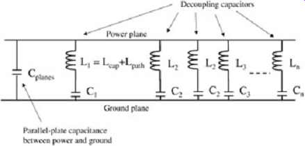
FIG. 14: Simplified model of a ground plane with decoupling capacitors.
From equation (12) it can readily be derived that the impedance will
be zero for the condition of (13).
At this point the capacitors are resonating with their own self-inductance plus the path inductance. This point is similar to the minimum impedance point seen in the capacitor curves in FIG. 13 except that there is an added inductive component in L1 from sources other then the capacitor itself. (The inductance of the capacitor itself is typically 1 nH for common surface-mount capacitors.) At frequencies higher than the series resonant frequency, the slope of the impedance curve for the given capacitor changes, meaning that the circuit has become inductive. Thus the circuit will present more impedance with higher frequency. Thus it is evident that the series inductance should be kept to a minimum. To put this in perspective, even a very close and low inductive path to a nearby decoupling capacitor on a standard PCB board can easily be 2 nH. One standard via is approximately for close power 0.7 nH; thus, if it takes two vias to connect a decoupling capacitor (one via down to the power plane, and one on the ground side of the capacitor), the inductance is 1.4 nH. This is assuming no inductance from the plane or any other source, such as a package power or ground pin. Thus, even a well-placed capacitor on a standard board may have a total series inductance of 3 nH (1.6 nH for the capacitor self-inductance). Assuming that the capacitance of the decoupling capacitor should be significantly more than the capacitance of the planes, with a 6 in. by 6 in. board with close power and ground planes (10 mils), this means that the value of the decoupling capacitance should be larger than approximately 4 nF. Calculating the resonance using a 6-nF capacitor with 3 nH of inductance reveals a zero at 38 MHz, above which the capacitor will become less and less effective. This is discouraging for high frequency decoupling. The mistake should not be made, however, that the capacitor is necessarily completely ineffective above the series resonance simply because the inductance is dominating the impedance. As long as the total impedance is less than the impedance without the capacitor present, the capacitor is providing some decoupling.
It can also be seen from equation (12) that the impedance will be infinite at the condition met in the equation …
(14)
This is a pole in the impedance equation. At this point, the plane capacitance is resonating in parallel with the combined series inductance of the decoupling capacitors. Note that increasing the number of decoupling capacitors increases the frequency of this pole. At this frequency, current cannot be drawn from the power/ground structure. Thus, decoupling has not only become ineffective, but has actually become destructive to the goal. This can be seen in FIG. 15, which shows a plot of the impedance of the bare board (modeled as a pure capacitor) superimposed on the impedance of the board loaded with decoupling capacitors.
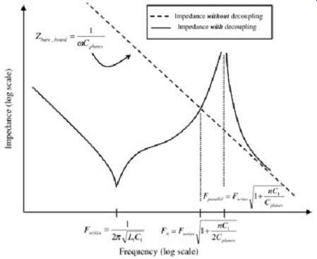
FIG. 15: Poles and zeros of a board populated with decoupling capacitors.
The frequency at which the impedance of a bare board is the same as the
board with the decoupling capacitors is given by the equation …
(15)
Beyond this frequency, the bare board impedance is less then the board loaded with decoupling capacitors.
The equations above can be derived assuming that all inductance and capacitance values of the decoupling capacitors are equal. In reality, of course, the values differ. There will, in fact, usually be several poles and zeros, due to the different series and parallel resonances for different inductance and capacitance values present. Equation (14) does not work for differing decoupling capacitors and/or differing inductance values. However, to estimate the general shape of the impedance curve, it is helpful to note that there is one parallel resonance between each pair of series resonances.
Two example cases are plotted in FIG. 16 with log-log scales. Superimposed on the plot is the impedance curve of the bare board if it were not populated with any decoupling capacitors. Very important, note that simply increasing the number of capacitors increases the frequency of the point FA (beyond which decoupling is ineffective). Thus a large number of capacitors is important to have in the system, preferably located close to the component to be decoupled. There will be distant capacitors (such as capacitors surrounding different components) that will contribute to the total decoupling; however, the inductance of the power plane may not be negligible at far distances. Furthermore, in the interest of minimizing loop area it is preferable to have the decoupling local.
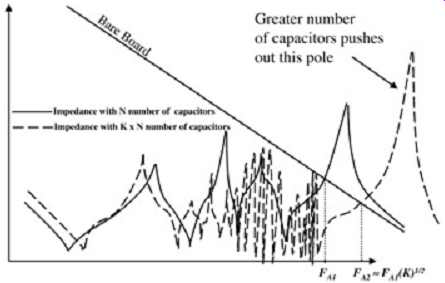
FIG. 16: Realistic impedance profile of a board populated with decoupling
capacitors.
Due to the series inductance inherent in the use of discrete capacitors, the decoupling network for a motherboard will become ineffective for frequencies that approach the pole described by equation (14). Depending on the implementation, this frequency can occur as low as 300 or 400 MHz.
A current area of study involves embedded plane capacitance in the board itself. Not surprisingly, these studies have shown far superior decoupling for these systems because the series inductance is very small. There are also several low-inductance capacitors available in the industry, such as "reverse" form factor surface-mount or interleaved capacitor packs. These devices are already used in some high-volume applications.
However, use of these capacitors require creatively minimizing the inductance of the placement on the circuit board, or the benefit is lost.
3.2. Choking Cables and Localized Power and Ground Planes
In Section 3.1 it was noted that decoupling high-frequency components might be infeasible. This situation creates an environment in which high-frequency noise propagates unhindered through a system creating a high probability that the noise will find an efficient radiator. Consider a high-frequency driver that induces noise onto the power and ground planes such as shown in FIG. 10. Since the high-frequency noise is not decoupled, it is free to propagate through a large number of paths. Often, the noise will access an external cable and radiate as a common-mode radiator. For this reason, inductive components are sometimes used to choke off the high-frequency noise. This is commonly done at cable connection points, as illustrated in FIG. 17 using board-mounted devices or ferrites that surround the outside of the cable. This technique is also sometimes used to choke off local power and/or ground regions containing noise sources as shown in FIG. 11. The inductive components used for such purposes are usually ferrites, which are lossy inductive components. The losses help minimize the magnitude of possible resonances as well as dissipate some of the noise energy.
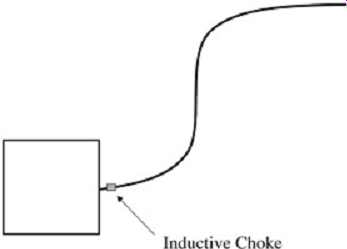
FIG. 17: Choking off noise coupled onto a cable.
When reference plane isolation is applied, the power and/or ground connections to the planes are made with an inductive component. The inductance will choke off high-frequency components. As described in Section 6, however, it is optimal from a signal integrity point of view to minimize the inductance to the power supply. Subsequently, there can be significant trade-offs in signal integrity and high-frequency power delivery capability. By solving an immediate problem, this method often creates different problems in signal integrity, power delivery, and even increases some other types of emissions. First, the inductive power can make it impossible for choked off components to operate in specification by starving the component from high-frequency power. Subsequently, the power/ground environment seen by the component will be much more noisy (see Section 6). Second, creating islands in the power or ground planes may imply that signal lines must cross over a gap in the reference plane, which causes other significant signal integrity problems (see Section 6). The method of localizing and choking off reference planes should not be excluded from consideration, but its trade-offs should be understood. Choking mechanisms for both external cable connections and, when absolutely necessary, for isolated power/ground regions are explored in the following two sections.
Choking Cable Entry Points.
A wide variety of inductive components are available to minimize common-mode noise on cables. These products include ferrites that fit around the cable itself (including ferrites that are deliberately split, which are meant to be retrofitted easily to a cable that is already in place), board-mounted ferrites, and even cables with ferrite material integrated. These components are available in high-or low-loss versions but are typically lossy. These ferrites work based on their physical property of high permeability µr (one manufacturer lists a range of 15 to 1800). The most typical application involves physically slipping a ferrite around the outside of a cable, thus effectively increasing the effective permeability seen by the cable and thus also increasing the series inductance. However, the inductance is seen only for common-mode currents because the magnetic fields from opposite currents will cancel (unless the two currents pass through different holes in the ferrite, as in multihole ferrites). For differential signals or a coaxial cable, the desired signals are not affected as long as the anticipated return path is being utilized. Thus, except for applications in which the current is flowing deliberately in only one direction, the ferrites affect only the undesired components of the current.
Although ferrite beads are generally thought of as inductors, they are in fact lossy transformers, which is consistent with their intended purpose of dampening high-frequency components. The impedance that the ferrite introduces can be modeled as a resistive component and an inductive component, as shown in the equation (16)
…where L0 is the inductance per length of the cable or wire under consideration, µe the effective relative permeability of the ferrite (listed by the manufacturer, typically a few hundred), l the length of the cable covered by the ferrite, and R the resistive (loss) component of the ferrite. The reader may have deduced from (16) that the inductance offered by the ferrite is (17).
For a coaxial cable, the inductance per length, L0, can be estimated from (µ/2p)ln(rshield/rinner conductor). Since the cable usually contains no magnetic material, the permeability is usually equal to that of free space, µ0 = 4p × 10-7
H/m. If the ratio of the radii of the coaxial cable is not known, they can be solved from the impedance formula ln(rshield/rinner conductor), which, except for cases with µr ? 1, usually results in Zo = 60(er) -1/2
ln(rshield/rinner conductor). If the dielectric of the cable is unknown, usually Teflon can be assumed with er ˜ 2.1. For 50-ohm cable, the ratio comes out to be about 3.6.
The impedance of the ferrite core is typically listed by the manufacturer and ranges from about 50 to 600 ?, more commonly in the range 100 to 200 ?. The impedances are generally listed at 25 and 100 MHz; however, the impedance curve is generally more complex and increases steeply with frequency. A typical impedance curve of a cylindrical ferrite used to slip over the outside of a cable is shown in FIG. 18. Such curves, which are provided by the manufacturer, should be used to determine the ferrite impedance at the desired frequency. The attenuation of the ferrite is (18a) where, Zs, ZL, and Zcable are the source, load, and ac resistance of the cable, respectively, and Zf is the impedance of the ferrite. For example, if a choke such as that depicted in FIG. 18 is slipped around a cable and the source and load impedance values are 50 ohm and the losses of the cable are neglected, the resultant best case attenuation at 100 MHz induced from the ferrite is approximated as (18b)
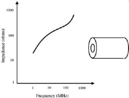
FIG. 18: Impedance variation of a ferrite core. Ferrite dimensions: inner
diameter, 8.0 mm; outer diameter, 16 mm; length, 28.5 mm.
The ferrite impedance at 100 MHz is determined to be approximately 250 ohm from the chart in FIG. 18. It can be seen that the ferrite can have a significant effect on common-mode currents and thus be very useful in prevention of common-mode radiation. Ferrites can be used with internal as well as external cables. It should be noted that if the ferrite is to be used for external cables on devices with a metal case, they should be placed as close as feasible to the actual boundary of the case of the device. If the ferrite is placed a distance inside the metal case, the cable can pick up noise after it passes through the ferrite. If the ferrite is placed a distance from the outside of the metal case, there will be a segment that can act as a good common-mode radiator.
One can improve the function of the ferrite by making multiple turns of the cable through the ferrite. However, this may bring the ferrite into saturation and reduce the inductive effects of the ferrite. Furthermore, the turn-to-turn capacitance may provide a bypass for high frequency components and negate the effect of the ferrite. The increase in impedance of the ferrite is proportional to the N2 , where N is the number of turns. A condition of saturation can be checked by using the equation (19)
to check the flux density, B. One manufacturer lists saturation levels ranging from 2800 to 3800 G (units of gauss must usually be converted to units of tesla; 1 T = 10^4 G). Using a typical permeability of a ferrite, µe = 1500, a maximum flux density of 3000 G (as provided in the data sheet), an inductance per length of a RG58/U cable (found as described above) of 260 nH/m, and the ferrite pictured in FIG. 18, the maximum current before the ferrite will saturate is found as follows:
Certainly for most applications this level of current will not be approached. The exceptions may be in power cables or in large parallel data cables. If multiple turns are made through the ferrite, the maximum current must be derated by N2. Inductive Isolation, Cutting Ground/Power Planes, and Star Grounding.
A method sometimes employed to minimize the effect of a noisy component coupling noise into a system where it may be radiated is to physically cut the ground and/or power reference planes and feed the localized power and/or ground through an inductive component. The idea behind this method is to isolate the high-frequency noise components generated by the device and prevent them from propagating through the system. In digital systems historically, this has frequently been done with the system clock chip. This is illustrated in FIG. 11. The method can be applied to just one plane or both the power and ground plane for a noisy component.