AMAZON multi-meters discounts AMAZON oscilloscope discounts
As mentioned previously, using this method has several detrimental effects in a high frequency digital system. Generally speaking, this method should not be considered unless other methods are exhausted or prior experience on similar systems suggests that this method is preferred or required, or unless there is another compelling reason. In fact, despite the disadvantages of this method, it is very frequently applied on computer motherboards.
To see the disadvantages and merits of this method, let us first consider an analogous method used primarily for lower-frequency designs (from the good old days) and still applied very successfully in systems containing primarily analog and audio circuits. In this technique, called star grounding, the 0-V references are tied to earth ground (chassis) at only one point in the entire system. This is similar to inductive isolation of reference plane regions in the fact that it minimizes the propagation of noise by the use of an impedance that isolates the noise from the larger ground structure. For star grounding the high impedance is an open circuit, due to the absence of an otherwise local ground connection, whereas for inductive isolation an inductive component is used for the impedance. In principle, the two techniques have a few common traits.
When distributed components of a system are tied together in a star-grounded fashion, the ground of each component extends all the way back to one central ground and has no local alternative path to chassis ground. In FIG. 19, two conditions are illustrated, one with the switch open and one with the switch closed. Components A and B can be different systems in different chassis, or different subsystems within a system. When the switch is closed, component B has a local dc connection to ground. When the switch is open, component B has no local connection to ground but still has some local parasitic capacitance to ground. The latter condition (switch open) is in the star-grounded configuration. At low frequencies, the star-grounded configuration has the advantage of having no extra ground loop since the potentially large loop between the local ground connections has been cut. Due to this, differential-mode emissions will be reduced. The star grounded condition also has the advantage of having only one 0-V reference voltage and is immune to differences in the local 0-V potential and induced differences from the large loop that would otherwise be present. All this works fine at low frequencies. However, recall that the differential emission envelope (FIG. 5), decreases above a certain frequency for large loop size. Thus, the large loop that was avoided by using star grounding will radiate in the differential mode primarily at lower frequencies, which are not usually the most difficult emission problem in a high-speed digital system. Furthermore, for smaller systems in which the ground loop avoided by star grounding may not be so large as to be purely a low frequency emitter, the capacitance to chassis ground at remote points (component B) can contribute to a resonance that can create an efficient radiator at high frequency. Even with no resonance, the capacitance closes the loop anyway, leaving no benefit of star grounding at high frequency. Finally, a distant ground, such as necessary for star grounding, will quite likely make the power delivery impedance too large for high-frequency current distribution.
Thus, although star grounding has several advantages at low frequency, it should generally not be done on a high-speed digital system unless there is a compelling reason. A motherboard, for instance, should have many connections to chassis ground and should have low-impedance ground and power paths throughout. This is true particularly near high frequency regions because without the dc path to chassis ground, a capacitive path to chassis may still be found and may excite a resonance. To summarize, in high-speed systems, avoid star grounding.
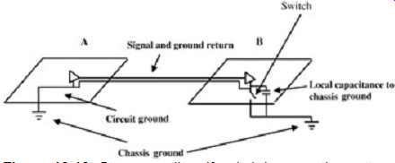
FIG. 19: Star grounding. If switch is open, the systems are star grounded.
The emission effects of star grounding can be seen graphically in FIG. 20. At low frequencies it can be seen that emission is reduced significantly; however, at chassis resonances, there may be large peaks. Not evident in FIG. 20 is the fact that star grounding could also increase the impedance in the power delivery path and cause large common-mode voltages due to voltage drops in the power delivery system. This could negate any emissive gains as well as ruin signal integrity.
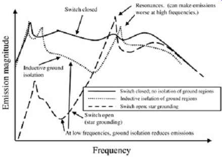
FIG. 20: Effect of star grounding.
Consider FIG. 11 again. The condition created is similar in many ways to that of star grounding. For instance, the power delivery is high impedance at high frequency (although this is an unintentional effect in star grounding). Also, the differential loop return has been disturbed with an impedance similar to star grounding in which the larger return loop was cut (although one may argue that it has instead caused any deviated current to return in a more labyrinthine fashion, thus increasing the loop area). Finally, similar to star grounding, there is a possibility of a capacitive return path that completes the cut loop for high frequency.
We have seen in Section 10.3.1 that high-frequency decoupling (above a few hundred megahertz) can be ineffective in a typical high-speed system. Thus, it is no surprise that the smaller power and ground regions in FIG. 11 may not be adequately decoupled. The lack of adequate decoupling will create a noisy environment for the isolated component, which will have a negative effect on signal integrity and may cause false logic triggers.
Furthermore, as already mentioned, if the ground and power planes are laid out such that the signal traces cross the gap in reference, more signal integrity effects will be introduced.
So, with all the negative effects of reference plane isolation, there exists the inescapable fact that it is sometimes the only feasible way to contain high-frequency noise that is causing a common-mode emission failure. In one case known to the author, a relatively strong memory clock buffer chip with 18 simultaneously switching outputs caused emission failures until the ground and power planes around the device were isolated and choked off with onboard ferrites. This particular example was very similar to FIG. 11. In this case all the outputs were 3.3-V 100-MHz memory clock outputs. The slowest rise and fall times for this particular device were specified to be about 1 ns. In retrospect, this problem should have been identified in the early architecture stages and should have been bypassed before it existed.
As a general rule, involve EMI engineers early in the design stage.
Several references suggest, as a way to reduce emissions, slowing the edge rate of the elements in the system that is causing the noise. It is certainly true that slowing the edge rates will result in reduced emissions, since slowing the edge rate will result in fewer high frequency components. However, there are many other variables inherent to a driver that may be of greater consequence. Furthermore, there is the fact that slowing the edge rates necessarily has a detrimental effect by increasing timing uncertainty in the system. Thus, slowing the edge rates should be done only as a last resort.
As a final note, measurements have shown that cutting ground or power planes in the manner shown in FIG. 21 has a minimal effect in containing high-frequency noise. No matter how "thin" the path to the "island," the inductance is not effective.
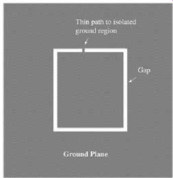
FIG. 21: Routed ground isolation: does not work to reduce emissions.
3.3. Low-Frequency Decoupling and Ground Isolation
As a rule of thumb, frequencies below 30-MHz noise will be transmitted primarily by conduction, and noise frequencies above 30 MHz will radiate. This is the reason that the radiated emission standards begin at 30 MHz, and below that frequency the compliance standards are considered conductive emissions.
It has already been noted that for low frequencies, star grounding has several benefits in minimizing noise. Thus the reader may have surmised that at low frequencies there is some advantage to be gained by isolating the ground and/or power planes of a low-frequency noise generator in order to contain the low-frequency noise. This is exactly the technique that will be advanced here. However, this method should be used only when necessary in a high-frequency system, and the trade-offs should be well understood.
In a case where low-frequency noise is causing a functional problem, or less likely an emission problem, the ground and power of the noise source can be isolated and effectively star grounded, unlike the rest of the system. Since high-speed systems typically have many ground paths to minimize ground impedance, low-frequency noise propagates very well through all dc paths in the system. To contain low-frequency noise, you simply cut the dc path. The only problem occurs when this affects the low impedance required for high-speed reference. Consider, for example, a low-frequency power source that dumps large amounts of current at a low frequency. The noise may already have its own separate power plane.
The question confronting the designer is whether to cut the ground plane underneath the noise source to prevent noise from propagating to the rest of the system. Standard high speed design practice says no. The standard design practice should certainly be adhered to if any high-frequency sources require a ground reference near the area to be cut. However, even if the cut is far away from any high-frequency reference point, cutting the ground decreases the total capacitance between the planes. The considerations contained in Section 10.3.1 regarding high-frequency decoupling should convince the reader that it is generally not preferable to cut the ground plane. However, there may exist cases in which the rule must be violated and the ground plane cut. There is some data to suggest that low frequency noise present in a system has an ill but elusive effect on system clocking. It is possible that low-frequency noise can interfere with the operation of phased-locked loops (PLLs), which are used for frequency stability in clock drivers and receivers. This noise can cause the PLL to modulate at the same frequency as the noise. At noise frequencies sufficiently high, the noise will be beyond the PLL bandwidth and there will be no problem. At noise frequencies sufficiently low, all the PLL in the system will respond to the noise and copies of the clock reference will modulate in a fairly similar manner. The worst-case condition is when the frequency is between a few hundred kilohertz and about 5 MHz, at which condition some of the PLLs in the system will modulate and some will not. This noncorrelated modulation of the clock reference can cause large variations in the timing reference. Such an effect is very difficult to measure. The final judgment is left to the designer. However, if the ground plane is cut, every precaution to minimize the area of the cut and the locality to high-frequency references should be made.
4. ADDITIONAL PCB DESIGN CRITERIA, PACKAGE CONSIDERATIONS, AND PIN-OUTS
Many of the aspects of board design for minimum emissions have already been mentioned.
The benefits of low-impedance ground and power has been mentioned, along with the fact that there should be many chassis ground points both to prevent resonances from the capacitance to chassis and to further reduce the ground impedance. The value of maximizing the inherent power/ground plane capacitance has also been mentioned.
Furthermore, it has been explained that traces should not cross gaps in the reference planes, particularly high-speed traces such as the system clock. Finally, the difficulties of high frequency decoupling have been explored. In this section we detail some additional criteria for minimization of emissions and system noise. It has been assumed that in all cases, boards with sufficient numbers of layers to have at least one fairly continuous plane for ground and one plane for power have been used. Furthermore, it has been assumed that all boards under consideration are of controlled impedance design (i.e., 50 ohm traces) and have been implemented with some sort of matched termination. The details for boards with 'routed' power and ground are not covered in this Section.
4.1. Placement of High-Speed Components and Traces
High-speed components should be placed ideally near the center of a mother-board, or at least far from the edge. Also, if a trace is routed near a vacancy in the ground plane, for instance, fringing fields, which would otherwise be referenced to ground, can radiate to space. These fringing fields can also capacitively couple to the chassis or other structures and excite a resonance. Similar arguments apply to vias in close proximity to high-speed traces and components. Vias cut the power and ground planes, resulting in a discontinuous plane. Their placement should be considered carefully.
4.2. Crosstalk
Crosstalk is typically considered as a signal integrity parameter, but it is also a parameter that affects the mobility of noise in a system. More crosstalk results in a higher probability that noise will find an efficient radiator, such as crosstalk to a trace that ultimately is routed to an external cable. Basically, by limiting crosstalk the number of paths that high-frequency components may take is limited, thus limiting the probability that a radiation mechanism will be excited. Although it is difficult to make statistical judgments, the designer should realize that less crosstalk will generally result in less radiated emissions. Consider a trace that feeds an external cable adjacent to another board trace, as shown in FIG. 22. Crosstalk can directly create common-mode noise on the trace feeding the cable and could potentially cause large emission problems.
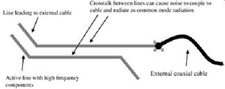
FIG. 22: Crosstalk to line feeding external cable.
Crosstalk falls off with conductor spacing exponentially. When the minimum spacing is being chosen, early in the design cycle, the crosstalk versus distance should be plotted. If the design is in the region where a small amount of increase in trace-to-trace distance will result in a dramatic decrease in crosstalk, increasing the spacing should be considered. Other variables that affect crosstalk, such as distance from ground plane, should be plotted in the same manner. Basically, if the crosstalk is in a "steep" portion of the graph, a little extra spacing should be an easy sell to the design team. Furthermore, target or known-sensitive traces can be picked, and the crosstalk on these traces can be minimized.
4.3. Pin Assignments and Package Choice
The pin assignment recommendations and package choice criteria of Section 5 should be adhered to. The importance of good power and ground pin selection for emissions compliance has to do with minimizing the impedance of power delivery to the silicon, minimizing the area of return path loops, and increasing the frequencies of harmful resonance effects. When possible, outputs of different frequencies should not share adjacent power or ground pins (and should not be placed next to each other). Furthermore, the pin out should be chosen with decoupling in mind. As described in Section 5, it is usually optimal to place power and ground pins adjacent to each other to increase the coupling between power and ground. In a case where it is known in advance that there will be a decoupling impossibility, the use of specialty low-inductance capacitors may be considered.
This may have an effect on the pin-out chosen.
5. ENCLOSURE (CHASSIS) CONSIDERATIONS
In this section we detail parameters of the box that surrounds the system or components therein.
5.1. Shielding Basics
Two basic mechanisms of shielding exist: reflection and absorption. These concepts, when applied to radiation, are not fundamentally different than reflection in transmission line systems. It is basically a matter of the wave impedance and the impedance of the shield. In the far field, where the wave impedance is 377 ohm, a conductor will look like a short circuit and reflect the wave much as it would do in a transmission line. Similarly, if a conductive shield is in the presence of a low-impedance radiator (current loop) in the near field, the shielding may not be effective because the wave impedance is low and the conductive shield looks like much less of an impedance discontinuity. Thus, the shielding effectiveness can be lower in the near field. However, the shield effectiveness can also be higher in the near field if the radiator is a high-impedance (voltage) radiator and thus may have a near-field wave impedance greater then 377 ohm. The equations in Section 10.2 are applicable here to determine wave impedance and near and far-field conditions.
Another parameter of interest when considering a conductive shield is the skin depth. The reader will recall that the penetration distance of a field into a conductor decays exponentially, e-x/d, where x is the distance beneath the surface of the conductor and is the skin depth, which is the distance at which the field has decayed to e-1 = 37% = -8.7 dB of the strength at the surface. FIG. 23 shows a field impinging on a shield. There is a reflection at the impedance discontinuity of the surface of the conductor and the opposite surface. The exponential decrease in field magnitude inside the conductor is also shown.
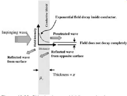
FIG. 23: Skin depth as a shielding mechanism.
Thus, depending on the thickness of the conductive shield, measured in skin depths, the amount of the field that penetrates the shield can be calculated. The shield effectiveness (SE) due to penetration offered for a sheet metal shield can be calculated as (20) where x is the shield thickness, in meters; ohm the resistivity of the shield, in ohm meters; µr the relative permeability of the shield material; d the skin depth of the material; and F the frequency of the wave.
From Table 4.1 the resistivity of copper is ohm Cu = 1.72 × 10⁻⁸ ?·m, whereas pure iron is ? Fe = 10 × 10-8 ?·m and steel ranges from 1.2 to 120 times the resistivity of pure iron. The relative permeability of iron and/or steel ranges from 110 to 14,800; however, ranges from 300 to 1000 are typically used for shielding calculations. Thus, although pure copper is more conductive (less resistive) then iron-based metals, the iron-based metals allow less penetration (recall that increased permeability decreases the skin depth). This is important except for conditions where the shield is thin (x << d). When the shield is thin, most of the shielding is accomplished due to reflection, and a higher-conductivity metal such as copper would be an advantage.
For materials other then sheet metal, such as conductor impregnated plastic, equation (20) is generalized as (21)…
…where q is a constant that varies with the conductive material or coating and x is the thickness. For conductive surface coatings, q will vary from 0.2 to 1.0. Reflection is, of course, the other parameter that determines shield effectiveness (SE).
Shield effectiveness due to reflection is defined as (22) where Zshield is the per square impedance of the shield (the same as the equivalent metal surface impedance in ohms per square for sheet metal, or this number is provided in data sheets for special shield materials), and Zwave is the wave impedance at the distance of the shield. Again, the shield effectiveness is a measure of the decrease in radiated emissions.
For wave impedance values much higher than the shield impedance, as is usually the case for conductive shields, equation (22) reduces to (23)...
…where the wave impedance is 377 ? in the far field or can be derived for the near field from equation (8) or equation (3), depending on the nature of the radiator. One can see that for low-impedance waves, such as in the near field of a low-impedance loop radiator, it may be difficult to get reflective performance from the shield.
Notice that unlike penetration performance, reflective performance from thin shields is not a function of frequency. Thus, thin conductive shields can be implemented successfully using primarily reflection as a shielding mechanism. The condition to avoid with such a shield is, of course, near-field low-impedance conditions. Conductor-coated, conductor-impregnated, or conductive plastics may also be used. These materials exist in several varieties, including particle-loaded plastic, fiber-impregnated plastic, carbon plastics, and plastic-coated screen.
The type can be chosen for the application in mind. For instance, due to the larger contact area between the conductive elements, fiber-loaded plastic can be had in a lower mass density than can particle-loaded plastics. Wear performance is another criterion. The reflective performance, however, is determined by the surface impedance Zshield.
The total shield effectiveness is calculated as (24).
5.2. Apertures
The shielding effect of an enclosure is only as good as its weakest link. It is no surprise that holes in the shield will often be the dominant variable in shielding effectiveness. Fortunately, there are techniques available to predict and to minimize the radiation from apertures in the shield. Some common reasons to have apertures are for viewing screens, thermal airflow, switch holes, cable holes, and mating seams, to name a few. In all cases, the amount of compromise of the shielding can reasonably be predicted, at least for worst-case values.
Typically, during the design stage, the dominant apertures (based on judgment) should be calculated in order to have a rough idea of the amount of shielding to count on. Calculating the worst case of every aperture in the design stage could lead to shield overdesign.
Rectangular and Circular Apertures.
Consider the rectangular aperture shown in FIG. 24. An impinging wave on the surface containing the aperture, and polarized such that the electric field is 90° to the direction of the slot, produces the worst-case noise transmission. In this case the opposite surfaces of the slot will look like a capacitor, and because current will have to flow around the slot, there will be an inductive component as well. Thus, much like a transmission line, the slot will look like an LC circuit and will have an impedance that depends on the slot dimensions. In fact, the panel with the rectangular hole can be thought of as a slot transmission line that is shorted on both ends, as suggested by the cross section of the panel side shown in FIG. 24.
The ratio of the slot impedance and wave impedance will determine the magnitude of the reflection coefficient and subsequently the shielding effectiveness. Equation (25) is a practical formula for computing the shield effectiveness of a slot [White, 1986]. Note that equation (25) must always be less than or equal to the shield effectiveness without a slot, as calculated in equation (24).
(25)
…where SEslot is the shield effectiveness of the slot, in decibels. SEshadow is the shielding performance due to the shadowing effect, depending on the location of the slot, the geometry of the enclosure, and the location of the radiator. This is explained below. SEWGBCO is the effect of the "deepness" of the slot. Deep slots will radiate less due to an effect known as waveguide beyond cutoff. This effect is also explained below. X and G are the length and width in meters of the slot, as shown in FIG. 24. F is the frequency under consideration, in hertz. The terms to the right of 157 dB constitute the effective slot leakage.
Equation (25) is also valid for a circular aperture if 2 dB is added to the 157 term. This comes from the fact that the area of a circle fitting inside the square made when X = G is 0.785 times the area of the square made by XG. 20log0.785 = -2 dB less area, and since less slot area results in more slot attenuation, the 2 dB should be added. It should also be noted that equation (25) is for the worst case, where the electric field is perpendicular to the slot. For cases where this is not true, the shield can be far more effective.
Equation (25) cannot be more effective than the box without the aperture, and cannot be lower (less effective) than (26)
Shadow Effect.
The shadow effect noted in equation (25) results from the fact that not all radiators inside the box are positioned well to radiate toward the slot. This is affected by the aspect ratios of the box relative to the slot position and the frequency of the radiation under consideration, and of course it is also affected by the slot size. To visualize the effect of shadowing, imagine shining a flashlight into a slot from outside the box. Where the light falls inside the box is the worst site to place a radiator. In reality, the flashlight example is not quite true, however, because electromagnetic waves of typical emission frequency passing through a slot will fringe and exhibit lobes.
The behavior of the radiation after it enters through the slot from outside the box will depend on its wavelength relative to the length of the slot. At low frequencies, where X < _/2 (or, in other words, F < c/2X, where X is the slot length and c is the speed of light), the wave will tend to stay within 120° radial from the slot. Thus, at low frequencies, radiators positioned inside the box at angles greater than 120° from the slot will have a significant shadow effect.
For positions at angles less than 120°, the shadowing effect will be minimal. This agrees with intuition, which says that the inside surface of the shield containing the slot is a well shadowed surface (180° away) and directly opposite the slot (90° away) is not a well shadowed surface.
At higher frequencies, the radiation pattern inside the box resulting from an impinging waveform outside the box will develop lobes of maximum and minimum radiation intensity.
The higher the frequency, the more lobes will exist. The lobes tend to decrease the shadow effect because they will bend around the corners. Above a frequency where X = 2_ (F > 2c/X), no shadowing effect should be considered.
The numbers shown in FIG. 25 can be used as an estimate for shadow effect for X = 3_/2 (or F = 3c/2X). For more precise estimates of the shadowing effect, other references provide tabulated data based on volume integration of the box volume in which the shadow effect can be looked up using the box dimensions and slot dimensions [White, 1986]. It is intuitive that shallow boxes can produce significantly more shadow effect than can a deep box. Similarly, small slots have significant shadow effects.
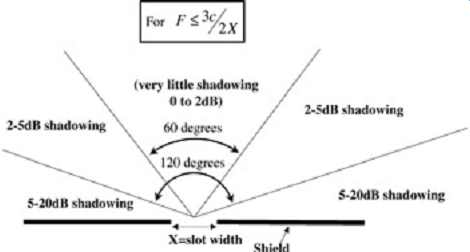
FIG. 25: Shadowing effect.
Waveguide Beyond Cutoff Effect.
When an aperture has a significant depth, it will begin to exhibit the properties of a waveguide. For frequencies less then the frequency necessary to excite the propagating modes of the waveguide, the depth will improve the shield effectiveness of the aperture. This is basically operating the waveguide below its operating frequency. This is known as the waveguide beyond cutoff effect. Waveguides have several propagation modes of operation.
If a frequency in a waveguide is below its dominant operating frequency, it is said to be in cutoff. Below the cutoff frequency, the radiation will be attenuated. Above the cutoff frequency, the radiation will pass relatively unhindered.
There are multiple cutoff frequencies for rectangular waveguides, depending on the mode of propagation being considered (derivations of these cutoff frequencies can be found in several electromagnetic textbooks). However, as an approximation, a dominant cutoff frequency can be calculated for a given aperture from the equation (27) ...
…where X is the length dimension of the aperture and c is the speed of light. Note that this in only an approximation to get a handle on the problem.
The effective shielding effect for frequencies below the cutoff frequency is approximated by (28).
Furthermore, equation (28) applies generally only when the thickness of the shield, t, has a significant depth compared to the slot dimension; thus t/X > 2. Above the cutoff frequency, there will be no shielding due to this effect. Thus, one way to increase the total shielding effectiveness [equation (25)] when apertures are necessary is to use thick shielding material or deep slots.
Modern chassis designs are usually made of thin sheet metal, so this effect is negligible.
Obviously, to use thicker metal would dramatically increase the weight and cost of the system. However, the innovative engineer may take advantage of the effect by using some kind of lightweight shielding material or by increasing the thickness of the shield only in the vicinity of apertures.
Screen Mesh.
The shielding offered by a screen mesh is calculated as (29) where S is the spacing between the wires in the mesh. Note that this equation is similar to (25). Seams.
Seams where chassis surfaces come together can be a source of leakage. The length of the seam is well defined; however, the width of the gap can vary widely. Judgment can be applied to estimate the gap width or the gap width can be measured with a feeler gauge.
Then the equations for slot apertures can be applied. If a conductive gasket is used, the leakage can be estimated from the vendor-supplied data.
Multiple Apertures.
Because the aperture leakages calculated in the preceding sections give values in decibels, the effective leakage of several apertures must be placed in linear units before adding them for a combined effective leakage:
(30)
…where Li_dB is the leakage effect in decibels of the aperture i as included in equation (25)
or a different appropriate equation. For example, if the leakage of an aperture is equal to Lhole = -3 dB, meaning that the hole degrades the shield effectiveness of the shield by 3 dB, four equal holes would degrade the shield by.
For apertures that are identical to each other, (30) reduces to (31)
…where N is the number of apertures.
An important observation to make is that emissions are reduced if one aperture is broken up into smaller ones. To see this, consider equation (25). Note that the leakage is proportional to slot dimension. If a slot aperture is subdivided into N smaller apertures, the improvement in shield effectiveness is calculated as (32).
5.3. Resonances
Resonance conditions in the system can compromise an otherwise good design and can result in very efficient radiators. All the features of the entire final structure are candidates for resonance, and the resonance conditions are not typically predictable. This is one of the reasons that the possibility of changes late in the design cycle is always a threat.
Unanticipated resonators could be heat sinks, chassis structures, resonant apertures, cables, traces, patches, or a wide variety of other structures. As a general rule, to avoid resonance, structures in the system should not be left floating. For instance, heat sinks should be grounded. The author knows of one incident where a system clock chip was located underneath a heat sink for a CPU. In this case the clock chip was coupling energy upward to the heat sink and causing a resonant condition. Increasing the distance between the heat sink and clock chip solved this problem. Although resonances are generally not predictable (i.e., the resonance of the heat sink did not seem to correlate to any particular dimension of the heat sink), it is very helpful to keep in mind that small structure changes can make big differences. A knack for applying trial and error is very helpful in this regard.
Resonant Slots.
One predictable resonance is that of a resonant slot aperture. At a slot length of _/2, the slot is resonant and can be considered a perfectly tuned dipole. This antenna will exhibit no shielding properties. This, along with the reasons discussed previously, is a good motive for keeping slot sizes small.
Losses.
Chassis resonances often dominate high frequency emissions. If resonances dominate emissions, the importance of making the resonances lossy, which will decrease the effective Q, can be seen. Often, this can be accomplished by placing lossy material inside the enclosure. When experimenting with such materials, it should be realized that a populated PCB board is itself a lossy component. Experiments, for example, of chassis resonances in the absence of a populated board will yield results that may not be as significant when a populated board is present in the system. Subsequently, when experimenting with lossy materials in the chassis, make sure that the fully populated board is included.
6. SPREAD SPECTRUM CLOCKING
A technique has recently become popular in high-speed digital designs known as spread spectrum clocking (SSC). SSC derives its emission benefits from slowly modulating the frequency of the system clock back and forth a small amount. Since many events in the system are synchronized to the clock signal (i.e., CPU circuitry is synchronized to the clock signal), changing the frequency of the clock results in many radiation mechanisms shifting in frequency, not just direct radiation from the clock circuitry itself. Thus, by slowly shifting the frequency of the clock back and forth, peaks in the frequency spectrum of operation of the system will move back and forth in proportion to the magnitude of modulation. In a time average (which is how the products are measured for emission compliance), the energy of the peaks will be smeared out and result in lower peaks. Thus, due to this smearing effect, peak emissions at any particular frequency will be reduced accordingly and will subsequently pass the emissions standard even though the total emitted energy is not likely to change.
This effect is shown in FIG. 26.
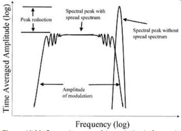
FIG. 26: Spectral content of the emission before and after spread spectrum
clocking.
The shape of the smeared spectral peak is determined by the modulation profile, that is, how the frequency varies between its modulation limits. It can be shown that one modulation profile that achieves a flat smeared spectrum, as shown in FIG. 26, is shown in FIG. 27, nicknamed the Hershey Kiss profile. Profiles other then this may have "rabbit ears" in the speared profile and thus not have as much peak reduction. The Hershey Kiss modulation profile is patented by Lexmark, however, and may involve some additional component cost (passed on from the clock vendor implementing this profile), due to royalties.
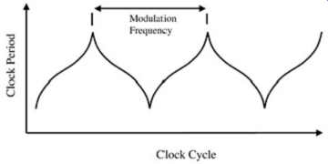
FIG. 27: "Hersey Kiss": clock modulation profile that produces
a flat emissions response.
One problem with clock modulation is that it can induce timing skew in the system phase locked loops (PLLs) that track the clock frequency in other parts of a computer system. In general, the slower the frequency changes, the less induced skew there will be downstream between all the PLLs. Thus, the Hershey Kiss profile is not optimal for tracking skew.
Because both sinusoidal and triangular modulation involve slower changes of frequency, either would be better for tracking skew but would not result in the maximum peak reduction benefit gained by Hershey Kiss. However, due to the gain in tracking skew using a non- Hershey Kiss profile, a bit more amplitude frequency variation can be introduced, yielding roughly equivalent benefits. As a de facto industry standard, the SSC modulation, if implemented, should be 0.6% down-spread (meaning that the clock frequency is varied only downward from the nominal) assuming a triangular modulation profile, or 0.5% down-spread assuming a Hershey Kiss profile. Each profile is shown in FIG. 28. The modulation frequency should be in the range 30 to 33 kHz (this modulation frequency is chosen to avoid audio-band demodulation somewhere in the system). Sinusoidal modulation profiles are generally not used because they exhibit a small spectral peak reduction. The reader should note that although SSC will decrease emissions, it will induce timing uncertainties into the system, especially in the phase-locked loops.
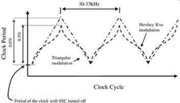
FIG. 28: Spread spectrum clocking profiles.