AMAZON multi-meters discounts AMAZON oscilloscope discounts
So far in this guide we have covered most of the issues associated with the PCB board. The basic fundamentals of a transmission line were explored in Section 2, Section 3 dealt with crosstalk, and in Section 4 we explained many of the nonideal transmission line issues with which modern designers must contend. Subsequently, we have explored in detail many of the issues associated with the electrical pathway from the pin of the driver to the pin of the receiver. The silicon, however, is located in a package, and the signal usually transverses through vias and connectors. In this Section we explain principles that will allow the designer to extend analysis to account for the entire pathway, from the silicon pad at the driver to the silicon pad at the receiver, by exploring packages, vias, and connectors.
VIAS
A via is a small hole drilled through a PCB that is used to make connections between various layers of the PCB or to connect components to traces. It consists of the barrel, the pad, and the antipad. The barrel is a conductive material that fills the hole to allow an electrical connection between layers, the pad is used to connect the barrel to the component or trace, and the antipad is a clearance hole between the pad and the metal on a layer to which no connection is required. The most common type of via is called a through-hole via because it’s made by drilling a hole through the board, filling it with solder, and making connections on appropriate layers via the pad. Other, less common types of vias, used primarily in multichip modules (MCMs) and advanced PCBs, are blind, buried, and micro-vias. FIG. 1 depicts a typical through-hole via and its equivalent circuit. Notice that the pads used to connect the traces on layers 1 and 2 make contact with the barrel and that there is no connection on layer 3. Blind and buried vias have a slightly different construction. Since through-hole vias are by far the most common used in industry, they are the focus of this discussion.
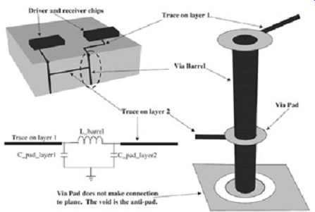
FIG. 1: Equivalent circuit of a through-hold via.
Notice that the via model is simply a pi network. The capacitors represent the via pad capacitance on layers 1 and 2. The series inductance represents the barrel. Since the via structures are so small, they can be modeled as lumped elements. This assumption, of course, will break down when the delay of the via is larger than one-tenth of the edge rate.
The main effect that via capacitance has on a signal is that it will slow down the signal edge rate, especially after several transitions. The amount that the signal edge rate will be slowed can be estimated by examining the degradation of a signal transmitted through a capacitive load, as shown later in this Section in equation (21). Furthermore, if several consecutive vias are placed in close proximity to one another, it will lower the effective characteristic impedance, as explained in Sect. 3. The approximate value of the pad capacitance is:
...where D2 is the diameter of the antipad, D1 the diameter of the via pad, T the thickness of the PCB, and er the relative dielectric constant. The typical total capacitance of a through hole via is approximately 0.3 pF. It should be noted that the via model depicted in FIG. 1 assumes that half of this total capacitance is attributed to each pad.
The inductance of the vias is usually more important than the capacitance to digital designers. The vias will add a small amount of series inductance to the system, which will degrade the signal integrity and decrease the effect of decoupling capacitors. The via inductance is modeled by a series inductor as shown in FIG. 1 and can be approximated by
...where h is the via length and d is the barrel diameter.
CONNECTORS
Connectors are devices that are used to connect one PCB board to another. As speeds increase, connector design becomes increasingly difficult. A good example of a high-speed connector in a modern digital system is the slot 1 connector used to connect the Pentium III cartridge processor to the mother-board. Another, more advanced example is the RIMM (Rambus Inline Memory Module) connector, which is operating at speeds of 800 megatransfers per second.
Since the geometries of connectors are usually complex, it’s impossible to accurately calculate the effective parasitics without the assistance of a two- or a three-dimensional field solver or measurements. However, the fundamental effects and a basic understanding of how a connector will affect system performance can be learned early in the design process by examining a first-order-level model.
In this section we examine the properties important to the design and modeling of high speed connectors by concentrating on the fundamental issues. The main topics explored in this section are connector crosstalk, series parasitics, and return current path inductance.
FIG. 2 depicts a conceptual connector that will be used to demonstrate the detrimental effects on signal integrity.
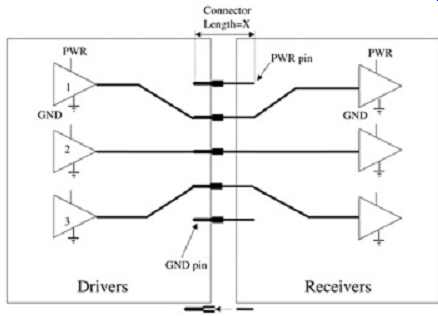
FIG. 2: Example of a PCB connector.
Series Inductance
The most fundamental effect of a connector is the addition of a series inductance, which can be estimated to a first-order level with the use of simple straight-wire formulas. Estimates for the series inductance of round and rectangular wire, respectively, are
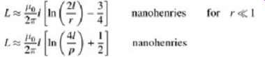
...where µ0 is the permeability of free space, l the length, r the radius of the wire, and p the perimeter. It should be noted that the length is the primary contributor to inductance; the shape of the conductor is not terribly significant as long as the cross-sectional width is small compared to the length.
Shunt Capacitance
Although shunt and mutual capacitance is also an important effect to consider in connector design, it can usually be ignored in the initial "back of the envelope" estimations of connector performance. The main effect that capacitance will have on the system is that it will slow down the system edge rate. It should be noted that the addition of extra capacitance is sometimes used to mitigate the impedance discontinuity seen at the connector. The addition of capacitance will lower the effective impedance of the pin. This must be analyzed very carefully and rigorously to guarantee that the design is sound. Extra capacitance can be added by using a wider pad, adding a small tab or widening out the connector pins. It should be noted that it’s difficult to estimate the effects of capacitance without the use of two- or three-dimensional tools or laboratory measurements.
Connector Crosstalk
Crosstalk also plays a significant role in connector performance. Typically, the mutual inductance plays a larger role than mutual capacitance. Subsequently, for first-order approximations, it’s usually adequate to ignore the mutual capacitance. When more accurate modeling is necessary, both two- and three-dimensional simulators, or measurements, can be used to determine accurate mutual parasitics.
The mutual inductance between two connector pins can be can be approximated as ...
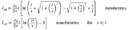
...where µ0 is the permeability of free space, l the length, and s the center-to-center spacing between the wires. It should be noted that the mutual inductance is largely independent on the cross-sectional area and the shape of the conductor.
Effects of Inductively Coupled Connector Pin Fields
Consider the connector in FIG. 2. The connector pins essentially form a network of coupled inductors. For the purposes of this exercise, we consider three drivers, one power pin, and one ground pin. The target will be net 2. The total induced voltage on pin 2 due to current changes in itself and pins 1 and 3 is ...
...where In represents dIn/dt. Assuming that the currents and the slew rates for each buffer are the same, a single-line equivalent model can be created to simplify the analysis:
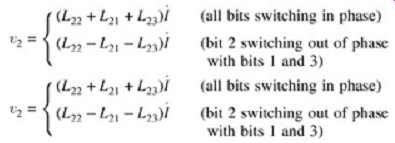
Equations above demonstrate how multibit switching through the connector pins can cause pattern-dependent signal integrity problems by inducing inductive noise onto the nets. However, what is often neglected is the effect of the power and ground connection pins.
Consider the circuit shown in FIG. 3. This is a typical configuration for a GTL + bus.
When output switches low, the N device is turned on and the P device is turned off. A high transition occurs in the opposite manner. Let's consider what the current does when the bus is pulled low by the N device. The current will be pulled out of Vtt and will travel through the transmission line, the signal pin, down through the N device, through the ground plane, through the ground pin, and back into the Vtt source.
This is depicted by the current loop in FIG. 3. Since a transient current will flow though the ground pin, it will induce inductive noise into the system of LgndI. Subsequently, the inductance of the ground return path must be considered in the analysis. This effect is magnified significantly if the return current from several buffers shares the same ground pin, as depicted in FIG. 4. In this particular case, the noise induced into the system would be 3LgndI, because three times as much current is flowing through the same ground pin. The same phenomenon holds true when transient current is flowing through the power pin. Care must be taken to understand how the return currents flow for the particular bus so that the effect of transient currents through the power and ground pins can be accounted for properly during the connector design. Various return current path scenarios for GTL and CMOS bus designs and their impact on the signal are explored in much greater detail in Section 6. It’s imperative that the return current paths be understood so that the connector design can be optimized.
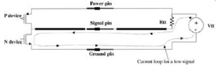
FIG. 3: Current path in a connector when the driver switches low.
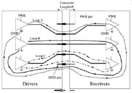 FIG. 4: Current path in a connector with several drivers.
For the time being, let's assume that the return current will flow entirely back through the ground pin as depicted in Figures 3 and 4. To derive the effect of an inductance in the current return path, refer to FIG. 5. FIG. 5a represents a system of three inductive signal pins coupled to an inductive ground return pin. Note that all of the current flowing through the three signal inductors must return through the ground inductor. The effect of the ground return pin can be represented as shown in FIG. 5b, assuming that the inductors are modified to include the inductive effects of the return path pin. This makes it easier to see the effect that an inductive pin in the ground return path has on the signal. The response of the system is shown in the following set of equations, which represent the response of FIG. 5a:
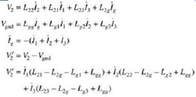
(9) is the voltage given by the simplified model. The result of (9) can easily be extended to a group of n conductors with a single current return path:
...where the voltage in FIG. 5b is given by...
Note that the effective inductance is simply the signal pin inductance, plus the ground return pin inductance, minus the mutual inductance.

FIG. 5: Incorporating return inductance into the signal conductor: (a)
three inductive signal pins coupled to an inductive ground return pin;
(b) effect of the ground return pin. It should also be noted that the
equations above are valid only for a coupled array of pins.
The total return path inductance will increase with distance from the corresponding signal pin and should be modeled separately assuming that the path is significantly long or the total return path inductance is much greater than Lgg. The total current return inductance is the sum of the pin inductance and the inductance of the path to and from the return pin. The larger the total loop area in which the current flows, the larger the inductance. For example, the total loop inductance of loop A in FIG. 4 has the largest total inductance, and loop C is the smallest.
Since the ground pins must return current to the power supply and the power pins must supply it to the drivers, low inductance is typically required for both power and ground paths to minimize inductive noise whether the return currents are flowing in the power or ground pins. Subsequently, it’s generally optimal to maximize the total number of power and ground pins to decrease the total inductive path. In the equations above, it will effectively decrease Lgg. Furthermore, it’s usually optimal to place power and ground pins adjacent to each other because the currents flows in opposite directions. Subsequently, the total inductance of the ground and power pins is reduced by the mutual inductance.
EMI
Another detrimental effect of a bad connector design is increased EMI radiation, covered in detail in Section 10. Notice the large current loops in FIG. 4. As explained in detail in Section 10, the area of the loop is proportional to the emission radiated. Connectors will also exacerbate simultaneous switching noise by increasing the inductance in the ground return path and signal paths. Simultaneous switching noise and ground return path analysis are covered in detail in Section 6.
Connector Design Guidelines
Based on the analysis above, several general connector design guidelines can be made.
The most obvious is to minimize the physical length of the connector pins to reduce the total series inductance. It’s also desirable to maximize the power and ground to signal pin ratio.
This will minimize the effect of the power and ground pin inductances. The placement of the power and ground pins should minimize the current loops and decrease connector-related radiated emissions. Each signal pin should be placed in close proximity to a power and a ground pin.
It should be noted that in cases where a large fraction of signals routed through a connector are differential, several of the design guidelines listed here will need modification. For instance, for connectors or packages that carry mostly differential signals, the number of power and ground pins required will probably be far less than those for a similar single ended system. Furthermore, differential signals may sometimes be grouped together in large banks without power or ground pins separating them.
Several conclusions can be drawn from the discussion above.
- __ Since coupling of signal pins to current return pins decreases the total inductance, it’s optimal that each signal pin be tightly coupled to a current return pin (by placing them in close proximity to each other). The bus type and configuration will determine whether each signal should be coupled to both a power and a ground pin, just a ground pin, or just a power pin. In Section 6 we discuss how to determine where the return current is flowing. If the return current is flowing in the ground planes, the signal pins should be coupled to the ground pins. If the return current is flowing through the power planes, the signal pins should be coupled to the power pins. If the return current is flowing through both planes, each pin should, if possible, be coupled to both a power and a ground pin .
- __ The power and ground pins should be placed adjacent to each other to minimize the inductance seen in the power and ground paths .
- __ It’s generally optimal to design a connector so that the ratio of power pins to signal pins and the ratio of ground pins to signal pins are greater or equal to 1. This will minimize the total return path inductance. This may not be as dominant a concern in differential systems .
- __ It’s generally optimal to use the shortest connector possible to minimize inductive effects and impedance discontinuities .
- __ It’s sometimes optimal to increase the connector pin capacitance to lower the impedance and minimize discontinuities. This can be achieved by widening the connector pins or by adding small tabs on the PCB .
- __ Connector capacitance tends to slow the edge rates .
RULE OF THUMB: Connector Design
- Minimize the physical length of the connector pins .
- Maximize the ratio of power and ground pins to the signal pins. If possible, these ratios should be at least 1 .
- Place each signal pin as close as possible to a current return pin .
- Place power pins adjacent to ground pins .
Example 1: Choosing a Connector Pin Pattern.
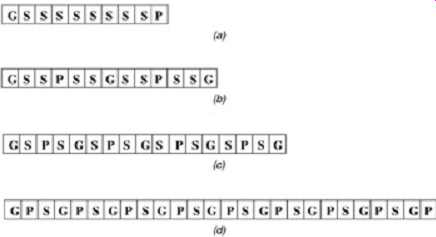 FIG. 6: Eight-bit connector pin-out options assuming return current
is flowing through both the power and ground pins: (a) inferior; (b)
improved; (c) more improved; (d) optimal. G, ground pin; P, power pin;
S, signal pin.
FIG. 6: Eight-bit connector pin-out options assuming return current
is flowing through both the power and ground pins: (a) inferior; (b)
improved; (c) more improved; (d) optimal. G, ground pin; P, power pin;
S, signal pin.
FIG. 6 depicts several pin-out options for an 8-bit connector. For the purpose of this exercise, assume that the return currents will be flowing equally through the power and ground pins. Option (a) will exhibit the worst performance because the power and ground pins are physically very far apart from the signal pins. This pin-out will maximize the inductive noise caused the power and ground return paths because the return currents flowing from each of the eight signals will have to travel through a single power or ground pin, which is very far away. Furthermore, since the power and ground pins are physically very far away from the signals, large current loops can exacerbate connector-related EMI and increase series inductance. Finally, since all the signal pins are adjacent to each other, pin-to-pin crosstalk noise will be maximized, which will degrade signal integrity. The only benefit of this pin-out is that it will be physically as small as possible and very inexpensive to manufacture.
Option (b) is an improvement on option (a) because the power and ground pins are physically closer to the signal pins. Furthermore, there are an increased number of power and ground pins which provide for lower-inductance current return paths and provide better power delivery. Pin-to-pin crosstalk is also reduced because the power and ground pins will provide shielding between signal pairs. The crosstalk between pairs, however, can still be quite high. Subsequently, this connector is an ideal solution for a four-bit differential bus.
Notice that the connector size has increased by 30% over option (a). Option (c) is a further improvement. Notice that both a power and a ground pin surround each signal pin. This minimizes the return current path inductance through both the power and ground pins. Furthermore, the intermediate pins shield the signal pins from adjacent signal pins and dramatically reduce pin-to-pin crosstalk between signals. Notice, however, that the size of the connector has increased by 70% compared to option (a). Option (d) is the optimal choice from a performance point of view (assuming that the return current is flowing in both the power and ground planes). Both a power and a ground pin surround each signal. Additionally, the power and ground pins are always adjacent to each other and the power/ground-to-signal ratio is 9 : 8. This minimizes the return current path inductance of both the power and ground pins, provides for significantly more shielding between the signal pins, and minimizes EMI effects. The obvious disadvantage of option (d) is that it’s 2.6 times larger than option (a). This example demonstrates that higher performance requires significantly larger connectors, which will affect the system in terms of cost and real estate. The designer must take great care in balancing performance with these constraints.
CHIP PACKAGES
A chip package is a holder for the integrated circuit. It provides the mechanical, thermal, and electrical connections necessary to properly interface the circuits to the system. There are many varieties of chip packages. The huge variety in packaging stems from the huge variety in system and circuit configurations. The number of different package types is growing constantly. Subsequently, it would be impossible to discuss each type of package that exists.
In this section we concentrate on problems common to virtually all chip packaging schemes and discuss modeling options so that any type of package can be modeled. Package design must be optimized for the type of bus. We explore the basic attributes that govern the performance of a package for both a point-to-point bus such as the AGP (advanced graphics port on a PC) and a multidrop bus (such as a GTL front-side bus on a PC with more than one processor).
Common Types of Packages
The physical attributes of a package can typically be separated into three categories: the attachment of the die to the package, the on-package connections, and the attachment of the package to the PCB.
Attachment of the Die to the Package.
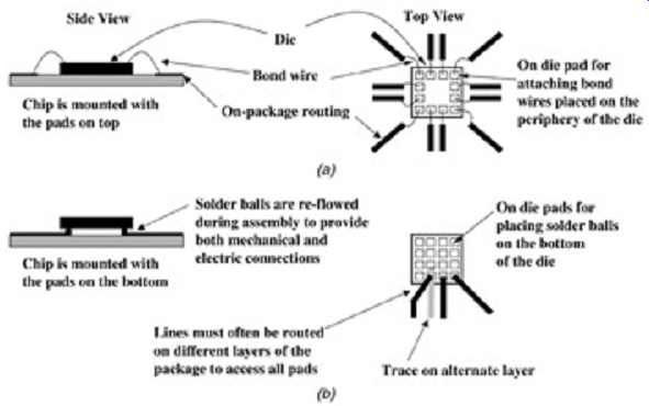
FIG. 7: Common methods of die attachment: (a) wire bond attachment;
(b) flip chip attachment.
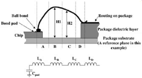
FIG. 8: Modeling the arch of a bond wire.
FIG. 7 depicts two of the most common methods of die attachment. Although many other techniques exist, these are by far the most common. First, let's explore the wire bond method of attaching the chip to the package. This is probably the most widely used method.
A wire bond is simply a very small wire with a diameter on the order of 1 mil. Just for reference, the diameter of a human hair is approximately 3 mils. The primary impact of a bond wire is added series inductance. Bond wire lengths vary from approximately 50 to 500 mils. Since bond wires are so short, they are often modeled as a discrete inductor. There are several methods of obtaining the equivalent inductance of a bond wire. Equation (3) can be used as a quick approximation; however, the most accurate means of bond wire inductance calculation requires that the arch of the bond wire and the proximity of the ground plane be accounted for. If there is no local ground or power plane, equation (3) is an excellent approximation. However, if the wire passes over a plane, it’s necessary to account for the arch and the height above the plane. FIG. 8 depicts the best way to do this. This particular example divides the bond wire into four sections. The first section, A, is roughly perpendicular to the reference plane; subsequently, the reference plane will have a minimal effect and its contribution to the inductance can be calculated with equation (3). Section B is roughly parallel to the reference plane with an approximate height of H1.
Subsequently, the inductance LB must be calculated using the inductance of a straight wire in the presence of a ground plane:
...where l is the length in inches, h the height above the ground plane, and d the wire diameter.
LC must be calculated in the same manner as LB using a height of H2. LD is calculated using equation (3) because it’s roughly perpendicular to the reference plane. To gain better accuracy, a two-dimensional field simulator should be used to calculate the inductance of each section instead of the equation presented here. A three-dimensional simulator would allow a more exact inductance calculation; however, it’s usually not worth the extra effort because the radius of the arch will change for each bond wire. Subsequently, any additional accuracy gained from the use of a three-dimensional simulator would be negated by the fact that it’s impossible to quantify the exact physical characteristics of each bond wire in the system.
Wire bonds also exhibit a large amount of crosstalk, which will cause pattern-dependent inductance values and ground return path problems that will be governed by equations (6) through (11). If there is no local ground plane, equation (5) can be used to estimate the mutual inductance between two bond wires. Otherwise, the following equation should be used to approximate the effect of a local ground plane :
...where L is the self-inductance of the two bond wires, s the center-to-center spacing, and h the height above the ground plane. A field solver should be used, however, to obtain the most accurate results. Furthermore, bond wires will tend to exacerbate rail collapse and simultaneous switching noise, which we explore in Section 6.
Although the use of bond wires leads to increased inductance and reduced signal integrity, the advantage is that they are inexpensive, mechanically simple, and allow for some changes in the bonding pad location and package routing. Furthermore, since the back of the chip is attached directly to the package substrate, it allows maximum surface area contact between the die and the package, which maximizes heat transfer out of the die.
Additionally, when using bond wires, the I/O pads tend to be limited to the periphery of the die, which will inflate the die size for a large number of I/O.
Now let's consider flip-chip technology. Essentially, it’s almost ideal from an electrical point of view. A flip-chip connection is obtained by placing small balls of solder on the pads of the die. The die is then placed upside down on the package substrate and the solder is re flowed to make an electrical connection to the package bond pads. The pads are connected directly to the package interconnects, as shown in FIG. 7. Flip-chip technology is also said to be self-aligning because when the solder is re-flowed, the surface tension of the solder balls will pull the die into alignment with the bond pads on the package.
The series inductance of a flip-chip connection is much lower than that of a wire bond. The typical inductance is on the order of 0.1 nH, which is an order of magnitude smaller than that of a typical bond wire. Furthermore, the effect of crosstalk in a flip-chip connection can be ignored. The bonding pads for a flip-chip connection can be placed over the entire die, not just on the periphery. This will help to minimize die size when a large number of I/O cells are required.
Mechanically and thermally, however, flip-chip technology is dismal. The thermal coefficient of expansion must be very close between the die and the package substrate. Otherwise, when the die heats up, it will expand at a different rate than the package, and the solder connections will be strained and can break. Furthermore, the physical tolerances must be very tight since the only degree of freedom when placing the chips is the small size of the pads. Cooling is also more difficult with flip-chip technology because the die is physically lifted off the package by the solder balls, which dramatically reduces the heat transfer and subsequently increases the cost of the thermal solution. Table 1 compares wire bonding and flip-chip technology.
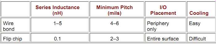
Table 1: Comparison of Wire Bond and Flip-Chip Technology: Series
Inductance (nH); Minimum Pitch (mils); I/O Placement Cooling; Wire bond;
Flip chip
Routing of the Signals on the Package.
The routing of the signals inside the package typically fall into two categories; controlled impedance and noncontrolled impedance. High-speed digital designs generally require the use of controlled-impedance packaging. A controlled-impedance package typically resembles a miniature PCB board with different layers and power and ground planes with a centered cavity used for die placement. The chip is usually attached with flip-chip bonding, although short wire bonds are often used. Small-dimensioned transmission lines are used to route the signals from the bond pad on the package to the board attachment. Controlled packages are significantly more costly than noncontrolled packages; however, they also provide for much higher system speeds. Noncontrolled-impedance packages usually wire bond the die directly to a lead frame, which is then soldered to the board. As one can imagine, this creates a series inductance that can wreak havoc on the signal integrity. FIG. 9 depicts some generic examples of controlled- and noncontrolled-impedance packages.
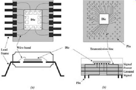
FIG. 9: Comparison of (a) a noncontrolled and (b) a controlled impedance
package.
Attachment of the Package to the Board.
Attachment of the package to the PCB is achieved in a large variety of ways. FIG. 9 depicts two popular methods, a lead frame (shown in the noncontrolled-impedance example) and a pin-grid array (shown in the controlled-impedance example). A lead frame is simply a metal frame that is integral to the package, which provides an electrical connection between the wire bonds and the PCB. It’s either attached with a through-hole mount or a surface mount. A through-hole mount is achieved by drilling a hole through the PCB, inserting the lead frame pins through the hole, and re-flowing solder. A surface-mount attachment is achieved by soldering the lead frame pins onto pads on the surface layer of the PCB. A pin-grid array (PGA) consists of an array of pins that stick out of the bottom part of the package. A good example of this is the familiar ceramic Pentium chip packages. Pin-grid arrays are often used with a socket because to allow the package to be removable.
There are other types of attachment techniques, such as a ball-grid array (BGA), which is attached to the PCB with an array of solder balls (a large version of flip-chip), and a land-grid array (LGA). Often there are two die mounted in a single package. The specific categories of packages are not covered in this guide. A good overview of chip packages can be found in Section 2 of Printed Circuits Handbook.
Creating a Package Model
Now that each basic part of a package is understood, let's explore the process of creating a package model. For the time being, we focus on the signals. The issue of modeling the power supply path to the die is discussed in Section 6. As mentioned before, the most accurate way to model a package is to use field simulators. Depending on the geometry, it may or may not require full three-dimensional analysis. If the design is largely planar, a two dimensional simulator will usually suffice. It’s important for the reader to remember that all the modeling lessons learned in previous Sections apply.
__ Examine each stage of the package and determine the fundamental components of the model.
__ Perform simulations with field solvers to determine the parasitics of each section.
Concentrate on groups of three to five lines so that the full effects of crosstalk can be accounted for.
__ Create distributed models of each section so that the model will behave correctly at the highest system frequency and at the highest system edge rate. If possible, use custom simulator elements such as HSPICE's W-Element to simplify the model and increase accuracy.
Example 2: Creating an Equivalent Circuit Model of a Controlled-Impedance Package.
Let's create an equivalent model of the controlled-impedance package in FIG. 10. This particular package has short bond wires to connect the die to the package electrically, and the connection to the board is a ball-grid array. Tracing the signal path from the driver to the PCB allows us to determine the various parts of the package that need to be modeled. In this particular example, it’s convenient to chop the problem into six sections: the silicon, the bond wires, the package routing, the via and ball pads, and the PCB traces. Usually, the capacitance of the on-die bond pads is provided by the I/O circuit designers. It’s largely a function of the transistor gate sizes at the last stage of the output buffer and by the capacitance of the ESD (electrostatic discharge) protection diodes.
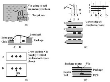
FIG. 10: Components of a package: (a) modeling a BGA package; (b) attachment
of die to package; (c) on-package routing; (d) connection to PCB.
Attachment of the die to the package. Tracing the signal path from the silicon, the first section to model is the bond wire array. To model the bond wires correctly, they are split into two sections because the beginning portion is roughly vertical and the second portion is roughly parallel to the reference plane (see FIG. 10b). The bond wire inductance can be estimated with the equations presented earlier, however, it’s more accurate to use a two- dimensional simulator to calculate the parasitics of each section. The cross sections of each section are shown in FIG. 10b. Once the mutual parasitics are known, the coupling factor, K, is calculated with equation. Coupling between bond wires should not be ignored because it can have significant impact. As a general rule of thumb, the inductance of a typical bond wire will be approximately 1 nH for each 50 mils of length. The capacitive parasitics of the bond wires have been ignored at this stage because they are extremely small and can usually be ignored. Although the power and ground bond wires are not included in this model, they can be dealt with in the same manner as power and ground pins in a connector array, as described earlier in this Section. This is explored in more detail in Section 6. The equivalent circuit is depicted on the left-hand side of FIG. 11, where C_pad chip is the I/O capacitance of the die, LA and LB are the bond wire inductance, and C_pad pack represents the bonding pad on the package (where the bond wire attaches to the package). Routing of the signals on the package. It’s usually adequate to consider either three or five coupled signals on a package because coupling effects tend to reduce very quickly with distance. It should be noted, however, that densely routed traces tend to couple to multiple traces as they wind their way from driver to receiver. Subsequently, it’s important to observe the package routing and determine which signals must be considered to achieve the nearest-neighbor coupling. In this particular example, trace 2 would be considered the target net, and lines 1 and 3 will be excited to account for crosstalk effects. The traces are separated into four sections represented by cross section A through D in FIG. 10c. In section A, all three lines are coupled; in section B, only lines 2 and 3 are coupled; in section C, lines 1 and 2 are coupled; and finally, in section D, only line 1 continues because it’s the longest. The package routing should entail all of the applicable effects outlined in Sections 2 through 4, including losses. Losses are often ignored in package designs, which is a mistake because small dimensions tend to make them significantly more lossy than typical PCB traces. The models of the package routes are shown in the middle of FIG. 11.
Attachment of the package to the PCB. This example is a BGA attachment. Subsequently, the major contributor to the performance will simply be the pad capacitance on the package and on the PCB. The via parasitics and the ball inductance will usually be small. The via parasitics can be estimated with equations (1) and (2). The ball inductance will usually be on the order of 0.5 nH. The only way to model the effect of the ball inductance rigorously is to use a three-dimensional simulator or to measure it. This section is shown on the right hand side of FIG. 11. Cvia and Lvia are the parasitics of the via that connects the package trace to the ball pad, Cball pad and Lball are the parasitics of the solder ball and pad, and Cball pad PCB is the capacitance of the attachment pad on the PCB.
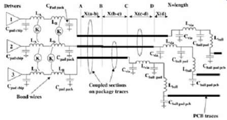
FIG. 11: Equivalent circuit developed for example.
Example 3: Modeling a Pin-Grid-Array Attachment.
A pin-grid array is a little easier to model but will still require the use of a full three-dimensional simulator to get the most accurate results. A good approximation of the pin inductance can be achieved with equations (3) and (5). To use these equations properly, the path of the current should be observed in detail. The total distance that the current travels in the pin should be used for the length. For an example, refer to FIG. 12. The inductance L_pin 1 is approximated using length X1 and the radius of the pin. The inductance L_pin 2 is approximated using length X2 and the radius of the plated through-hole. The entire radius of the plated hole is used because solder is re-flowed into the hole, making it a solid conductor.
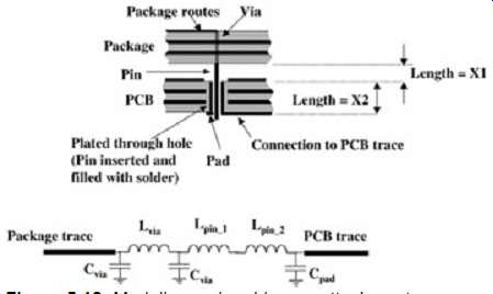
FIG. 12: Modeling a pin grid array attachment.
Effects of a Package
The effect that a package has on system performance dependent on both the electrical attributes of the package and the type of bus in which it’s used. In this section we explore the fundamental effects that a package will have on both a point-to-point and a multidrop bus.
It should be noted that other effects, such as simultaneous switching noise, are covered in Section 6.
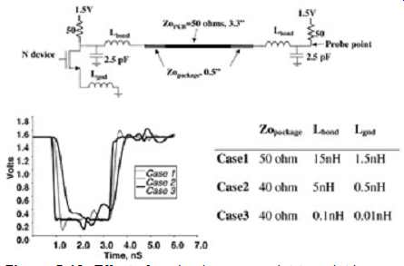
FIG. 13: Effect of packaging on a point-to-point bus.
Point-to-Point Bus Topology.
To demonstrate the effect of a package on a point-to-point topology, consider the following three cases depicted in the circuit in FIG. 13.
-- Case 1: noncontrolled-impedance package with a total bond length (bond wire plus lead frame) of 0.75 in.
-- Case 2: controlled-impedance package with 0.25-in. bond wires and a 40-? transmission line on the package
-- Case 3: controlled-impedance package with die flip-chip attached to the package and 40-? package routing
The test cases were chosen to be a simplified representation of a noncontrolled-impedance package, a controlled-impedance package with short bond wires, and a controlled impedance package with flip-chip attachment on a basic GTL bus. Notice that the cleanest waveform is achieved with the flip-chip attachment (case 3). Since chip package routing is often lower in impedance than the motherboard (due to the manufacturable aspect ratios in many package designs), the package impedance was chosen to be 40 ohm. Case 2 is identical to case 3 except that the flip-chip attachment was replaced with 250-mil bond wires represented by the 5-nH inductors. Notice that the edge rate has been slowed significantly due to the extra inductance. This is because the inductance will act as a low-pass filter, which will attenuate the high-frequency components. Also note the decrease in the general signal quality due to the inductive noise. Finally, case 1 represents the noncontrolled impedance by eliminating the 40-ohm package section and replacing it with a 15-nH inductance.
The 15 nH of inductance comprises the total inductance of a lead frame and a bond wire.
Note that the edge rate has decayed even more significantly, and there is considerably more inductive noise to contend with. In a full system simulation, the package inductance can wreak havoc on signal integrity and timing budgets. Crosstalk between bond wires and leads cause significant pattern-dependent inductance values (due to the mutual inductance), which will cause edge-rate differences and degrade timing margins. Furthermore, crosstalk and inductive ground and power paths will cause simultaneous switching noise, as detailed in Section 6.
Multidrop or Daisy Chain Topologies
Multidrop bus topologies are very common. Two common examples are the front-side bus on a computer system connecting a chipset with multiple processors and RIMM memory modules. A block diagram of a multidrop bus is shown in FIG. 14. The effect of packaging on such bus topologies is largely dependent on the package stub length. If the package stub is long, it will induce transmission line reflections that degrade the signal quality. If the package length is short, it will produce significant filtering effects that degrade the edge rate and change the effective characteristics of the transmission line.
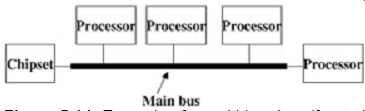
FIG. 14: Example of a multidrop bus (front-side bus). Processors are
tapped off the main bus.
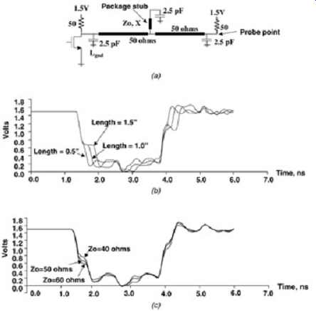
FIG. 15: (a) Circuit; (b) effect of package stub length, X; (c) effect
of package stub impedance.
Long Package Stub Effect.
A package stub is considered to be long if it meets the following conditions: ...
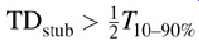
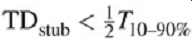
...where TD_stub is the electrical delay of the unloaded package stub and T_10-90% is the rise or fall time of the signal edge.
FIG. 15 shows a three-load topology driven from one end. Each capacitor represents the capacitance to the input stage of a receiver. The effect of package stub length and impedance is shown. Note that as the package stub length is increased, a ledge begins to form in the edge of the signal and increases the effective delay of the net (sometimes referred to as a timing push-out). The length of the ledge depends on the electrical delay of the stub. It should be noted that the capacitive loading at the end of the stub will increase the effective electrical delay of the stub by approximately 1 time constant (ZoC). It should also be noted that the package stub does not induce a timing push-out in the form of a ledge if its delay is significantly smaller than the rise or fall times. This leads to a good rule of thumb which says that the electrical delay of the package stub, including the receiver capacitance, should be small compared to the rise or fall time.
Example 4: Calculating the Effect of a Long Package Stub.
The response of a system with a long stub is easy to calculate using simple techniques explored in Section 2. If the system has more than one stub, however, it’s advisable to use a computer simulation. FIG. 16 shows a simple system with one stub. The first reflection is calculated below. The entire response can be calculated using a lattice diagram. The reflection coefficient looking into the stub junction is calculated as.
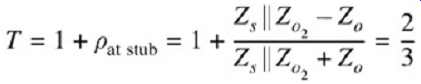
The impedance looking into the junction will be a parallel combination of the stub impedance Zs and the trunk impedance.
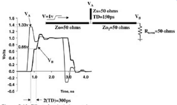
FIG. 16: Effect of a single long stub.
The transmission coefficient down the stub and the second half of the trunk is shown as.
Remember that current must be conserved; voltage does not. Subsequently, if the sum of the voltage transmitted down the stub and the second half of the trunk exceeds the input step voltage, don't be alarmed. Subsequently, the voltage from the first reflection at node B of FIG. 16 is
The voltage from the first reflection at node A is ...
...which is doubled because there is no termination on the stub.
As shown in FIG. 16, the timing push-out caused by the stub at node B depends on twice the total delay of the stub (the time for the signal to travel down the stub and for the reflection to come back).
Widely Spaced Short Package Stub Effect.
A package stub is considered to be short if it meets the following conditions: ...
...where TDstub is the electrical delay of the unloaded package stub and T10-90% is the rise or fall time of the signal edge. When a package stub is sufficiently short, the load will look like a capacitor. The total capacitance will be the sum total of the I/O capacitance of the silicon and the capacitance of the stub. For a single capacitive load in the middle of a transmission line, such as that shown in FIG. 17, the response can be calculated by plugging the parallel equivalent impedance of a capacitor, as calculated in equation (18), and inserted into equation (9).
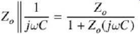
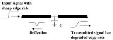
FIG. 17: Effect of a short capacitive stub.
The reflection and transmission coefficients are ...
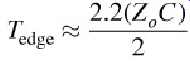
Note the form of equation. As the capacitance increases, the transmission coefficient decreases for a given frequency. This causes a low-pass filtering effect that will remove high-frequency components from the input signal. Subsequently, the signal transmitted through the shunt capacitor will have a degraded edge rate. Assuming a very fast input edge rate, the transmitted edge will have an edge rate approximately equal to 2.2 time constants (assuming 10 to 90% rise or fall times) between half the transmission line impedance and the value of the capacitance:
As described in Section C, equation (21a) assumes that the input edge is a step function.
To estimate the rise or fall time of the signal after it passes though the capacitive load, the equation ... (21b) ...should be used, where Tinput is the edge rate transmitted into the capacitive load.
Distributed Capacitive Loading on a Bus (Narrow Spacing).
When the package stub length is short compared to the edge rates [so they look capacitive and conform to equation (17)] and loads are uniformly distributed so that the electrical delay between the loads is smaller that the signals rising or falling edges, the effect becomes distributed instead of lumped. A good example of this is a RIMM memory module. The loading essentially changes the characteristic impedance and the propagation velocity of the transmission line. FIG. 18 depicts a distributed capacitive load due to several taps on a transmission line. The following equations are the equivalent impedance and delay parameters for a uniformly capacitive loaded
FIG. 18: Effect of distributed short capacitive stubs.
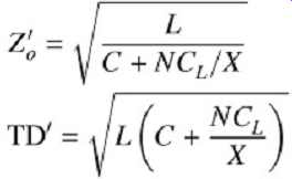
....where L and C are the distributed transmission line parasitics as described in Section 2, CL the total load capacitance (package stub + I/O), N the number of loads, and X the line length over which the loads are distributed. It should be noted that the capacitive loading will also have a significant low-pass filtering effect on the edge, as depicted in FIG. 18. Several conditions other than packaging will cause this effect, such as narrowly spaced vias and 90° bends.
Optimal Pin-Outs
Optimal package pin-outs are chosen in largely the same manner as connector
pin-outs, as described in Sect. 2. However, before a package pin-out
is finalized, it’s extremely important to perform a layout study to ensure
that the pin-out chosen is routable. In some applications, pin-to-pin
parasitic matching is more important than minimizing total pin parasitics.
For instance, in applications in which pin-to-pin skew is a critical
concern, a square package with pins on all four edges might be a better
choice then a rectangular package with pins on only the two longest edges.
This may be true even if some or all of the pins in the rectangular package
may have smaller parasitic values. This is because the square package
can be designed to take advantage of fact that its shape will allow less
difference in lead frame length to the pins. This might lead to better
performance even if the total parasitic per pin is greater for the square
package then for several of the pins on the rectangular package, which
is likely to have a larger relative difference in parasitics between
the corner pin and a pin in the middle. This is illustrated in FIG. 19.
Similarly, when choosing pin-outs in a rectangular package, the pins closer
to the middle of the package should be used for the highest-frequency
or most critical signals, as these pins will have the least parasitic
values.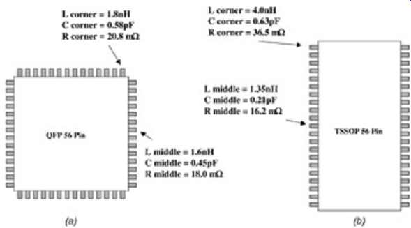
FIG. 19: Package examples: (a) good pin-to-pin match; (b) low parasitics on best pins.
RULES OF THUMB: Package Design
-- Avoid the use of noncontrolled packaging for a high-speed design.
-- Minimize inductance by using flip-chip or the shortest possible bond wire lengths for die attachment.
-- Follow all the same pin-out rules of thumb as described for connector design when choosing power and ground pin ratios.
-- Use the shortest possible package interconnect lengths to minimize impedance discontinuities and stub effects.
-- On a multidrop bus, stub length is often the primary system performance inhibitor.
-- In a multidrop bus design, never use long stubs that are narrowly spaced.
-- Pin-to-pin package parasitic mismatch, which is strongly affected by the physical aspect ratio of the package, should be considered.