AMAZON multi-meters discounts AMAZON oscilloscope discounts
1. ARITHMETIC CIRCUITS
We are all familiar with the rules of simple addition regarding the 'carry'. Here is an example of an addition sum an 8-year-old might do at school:
1 9 7 7 5 +
7 4 2
2 0 5 1 7
1 1 1
The child puts in the 'carries' below the answer line (so do I!) as a reminder that there is a figure to be carried from the previous column. Actually, even the child is doing the calculation in short-hand. The long way is to do the sum as two half-additions, like this:
1 9 7 7 5
+
7 4 2
1 9 4 1 7 PARTIAL SUM NUMBER ONE
1 1 CARRIES FROM FIRST HALF-ADDITION
1 0 5 1 7 PARTIAL SUM NUMBER TWO
1 CARRIES FROM SECOND HALF-ADDITION
2 0 5 1 7 SUM
The operation to add the first lot of carries is performed to provide the second partial sum; but this produces its own 'carries', which are added in to provide the answer. The same principle, that of using two half-addition operations, can work equally well with binary arithmetic, and is the method used in digital systems to add two binary numbers together.
Here is the calculation to add two binary numbers, the binary equivalents of(denary) 103 and 18: 1 1 0 0 1 1 1 1 0 0 1 0 + 1 1 0 1 0 1 1
PARTIAL SUM NUMBER ONE CARRIES FROM FIRST HALF-ADDITION
1110001 PARTIAL SUM NUMBER TWO CARRIES FROM SECOND HALF-ADDITION 1 1 1 0 0 1 SUM
The sum is the binary equivalent of (denary) 121.
If you look at the first three lines of the sum, you can detect a simple set of rules at work for binary addition:
0 + 0 gives 0
0 + 1 gives 1 1 + 1 gives 0 plus a 1 in the next column as a carry
This kind of rule can easily be applied with logic gates, and the function can be implemented with an AND gate with an EX-OR gate (see Fig. 1).
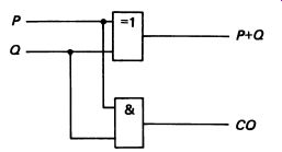
FIG. 1 a half-adder
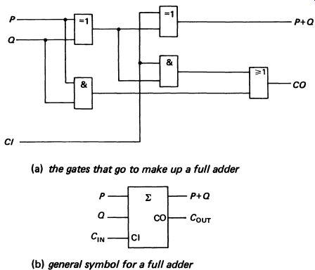
FIG. 2 (a) the gates that go to make up a full adder (b) general symbol
for a full adder
In the diagram, P and Q are the inputs, P+Q is the sum, and CO is the carry to the next column. Two half-adders can be combined to produce a full adder, which carries out the two operations, adding the two numbers and also the carry from the half addition. The circuit will, of course, accept a carry from a preceding stage, if there is one. To implement this, two half adders and another OR gate are required (see Fig. 2a). In the diagram P and Q are the inputs, CJ1 N is the carry from the pre ceding stage, P+Q is the output, and CO is the carry to the next stage.
The full adder is given a simplified symbol, shown in Fig. 2b. In a real system, such as a computer, 8-bit or 16-bit numbers will have to be added together, so full-adder stages are connected as shown in Fig. 3; this illustrates a 4-bit adder, for simplicity.
The two 4-bit binary numbers to be added together are gated (i.e. applied via logic gates) on to the adder inputs P0 -P3 and Q0-Q3 . The sum of the two numbers appears at the outputs P+Qo-P+Q3 , and if there is a carry out of the 4-bit sum, the carry appears as a logic 1 on C:OuT
Note that CIN is connected to 0 (no carry) if there is no preceding stage. This type of adder is called a parallel adder, because all the bits in the number are added together simultaneously. It is a fast method of adding binary numbers, and is the method used in computers. There are certain modifications that can be made to increase the speed even further, but such systems are well beyond the scope of this guide.
The other sort of adder is a serial adder. The same full adder is used, but the two binary numbers are pushed through, one digit at a time, out of shift registers (rather like a sausage-machine). Each pair of digits is added, and any carry is delayed until the next pair of digits is processed.
The shift registers are all controlled by the same clock pulse (as we saw in Section 21), and a single D-type flip-flop (see Figure 21.12) operated from the clock pulses will operate as a suitable delay.
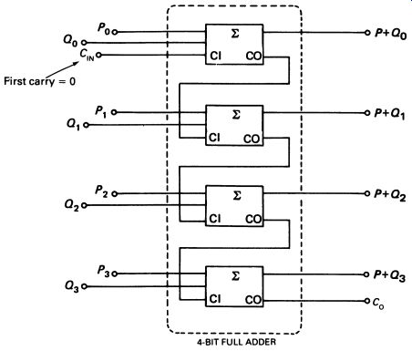
FIG. 3 a 4-bit parallel full adder.
Binary subtraction is accomplished by a process of first converting the number to be subtracted into its negative form, and then adding them together. To convert a denary number into a negative value, we have to subtract it from zero. Thus the negative form of 42 is:
0-42 = -42
Converting a binary number into a negative form is done by producing what is called the 2's complement (two's complement). This is done in two stages:
1. All the bits in the number are reversed, 0 for 1 and 1 for 0.
2. 1 is added to the lowest bit.
As an example, we can subtract 18 from 103 (they were added above, so it is possible to compare the calculations). The binary equivalent of 18 is 10010, but, when taking the 2's complement, we must consider all the values stored in the computer's register. Assuming that it is an 8-bit register, the contents will actually be 00010010, the first three 'leading zeros' being just as important as the rest of the number. In the same way, the binary equivalent of 103 is stored as 01100111, with a leading zero to complete the eight bits (which must, of course, be either zero or one). Using the rules above, the 2's complement of the equivalent of 18 is:
0 0 0 1 0 0 1 0 BINARY EQUIVALENT OF 18 11101101 REVERSE BITS 1 ADD 1 1 1 1 0 1 1 0 0 PARTIAL SUM NUMBER ONE 1 CARRY FROM FIRST HALF-ADDITION 1 1 0 1 1 1 0 PARTIAL SUM NUMBER TWO (NO) CARRY FROM SECOND HALF-ADDITION 1 1 1 0 1 1 1 0 2'S COMPLEMENT Now we can add the 2's complement of 18 to 103:
0 1 1 0 0 1 1 1 BINARYEQUIVALENTOF103 1 1 1 0 1 1 1 0 2's COMPLEMENT OF BINARY EQUIVALENT OF 18 1 0 0 0 1 0 0 1 PARTIAL SUM NUMBER ONE 1 1 1 1
0 1 0 0 0 1 0 1]010:0101
CARRIES FROM FIRST HALF-ADDITION PARTIAL SUM NUMBER TWO CARRIES FROM SECOND HALF-ADDITION SUM
The final carry has nowhere to go in the 8-bit register, and so is lost.
Binary 01010101 is (denary) 85, which is the correct answer to the original subtraction calculation, 103 -18 = 85.
In implementing the system in digital logic, NOT gates (inverters) are used to reverse the bits. Adding the 1 to the lowest bit is carried out equally simply, by feeding a carry into the first carry input-held, you will recall, at logic 0 (applied to CIN) during addition.
A 4-bit binary parallel subtracter is shown in Fig. 5.
It is straightforward to design a logic system that will add or subtract.
Serial subtracters are available, but are of course slower than parallel subtracters.
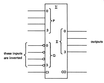
FIG. 5 a 4-bit parallel subtracter
It is possible to design systems for binary multiplication and division, and such systems are sometimes used in digital devices. However, the implementation is rather complicated and, at least in computers, the process of repeated addition is used instead of multiplication, and the process of repeated subtraction for division.
This part of Mastering Electronics is not intended to be a comprehensive description of arithmetic circuits, but rather to illustrate the way that binary numbers can be manipulated arithmetically by relatively simple logic systems. The operation of calculators and computers depends on this type of circuit. For a fuller description of logic circuits of all types, including arithmetic circuits, see Digital Electronic circuits and Systems by N. M. Morris (Macmillan, 1974).
2. ALGEBRA FOR LOGIC
Before leaving the topic of logic gates, mention should be made of techniques that are available for the minimization of networks. Systems consisting of a relatively few logic gates can be designed without too much trouble, and where the system can be simplified it is usually obvious.
Where large numbers of gates are involved, it is often far from obvious, and formal methods have been developed to help.
Often writing down the truth table for the system is enough, but an algebraic method, using a system known as Boolean algebra, provides a better method.
An alternative procedure in which all the conditions possible in the truth table are mapped visually can lead to a more rapid solution. The technique is called Karnaugh mapping.
Both systems are discussed in detail in more specialized books than this one, including Digital Electronic Circuits and Systems by Noel Morris.
3. COMPUTER MEMORY CIRCUITS
One of the requirements of a computer system is circuits that will store very large amounts of binary data. The computer memory has to hold many 8-bit or 16-bit binary numbers, available for instant recall by the computer. Even a small personal computer could have a memory system capable of holding at least 390 000 binary digits (bits), so clearly the circuits used have to be economic.
Early computers used a system called core storage in which each bit was stored in a ferrite ring, which could be magnetized (1) or not magnetized (0). Core storage was bulky and expensive, each ferrite ring having to be threaded on to a system of wires by hand, rather like weaving. Inside the computer's arithmetic unit, numbers were held in bi-stables.
With the coming of microelectronics it became possible to use bi-stables for all the computer's memory, and ferrite cores are now found only in museums-just a couple of decades after they were introduced.
The main memory of a computer is called the random access memory (RAM). An array of bi-stables is organized so that any one bistable can be separately accessed, or addressed. A standard small RAM chip would hold 1024 bits, organized in a two-dimensional array 32 x 32. This is shown in Fig. 6.
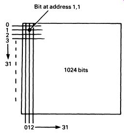
FIG. 6 a two-dimensional array that can access 1024 bits
A 10-bit binary number is sufficient to define any one of the 1024 bits.
There are 32 possible combinations of Os and 1 s in a 5-bit binary number (25 ) and two 5-bit binary to 32-line decoder systems can be used to obtain the required two-dimensional co-ordinates (see Fig. 7).
Fig. 7 two 5-to-32/ine decoders are used to address the 32 x 32 array by means of binary numbers
Additional logic is used to (i) set or unset (1 or 0) the bistable, according to the state of an input line (one for the whole array); or (ii) read the state of the bistable and apply it to the data line. The 'set/unset' or 'read the state of the bistable' selection is controlled by the state of an input to the system called the READ/WRITE input. The data input/output is called the DATA line. There is also a third control line called CHIP SELECT, which can disable the entire read/write system. A block diagram of the whole system is shown in Fig. 8.
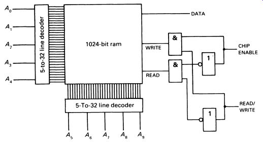
FIG. 8 system diagram for a 1024 x 1 bit RAM.
The system is intended to provide a memory of 1024 bits for a single position in an 8-bit (or 16-bit) binary register. There is only one data input/output, but according to the address that appears on A 0 to A7 (Fig. 8) that data line can be directed to any of the 1024 bi-stables.
A complete memory for a computer with an 8-bit binary input/output can be produced by using eight identical circuits like the one in Fig. 8, known as a 1024 x 1 bit RAM. All the address lines for the eight systems are simply paralleled so that corresponding elements in the eight memories are addressed at the same time. The data input/output lines of the RAMs are connected to different positions in the 8-bit computer data input/ output to provide 1024 8-bit binary numbers. The READ/WRITE lines are paralleled as well, so the computer can either read the memory, one 8-bit number at a time, or write data into it.
The 1024 x 1 bit RAM is rather small these days. Most computers use chips that have more memory on them. For example, the 6116 CMOS RAM provides 2048 x 8 bits (16 384 bistab1es) on a single chip. RAM chips containing 8192 x 8 bits (65 536 bistables) or 65 536 x 1 are used in modern designs.
The usual type of RAM is the static RAM, available in TTL or CMOS form. Both types are widely used; the CMOS scores, as usual, in having very low power consumption, but the TTL has a faster access time, the time it takes to read or write information into the memory. The access times vary, but are in the region of 100-500ns, with the TTL at the fast end of the scale_ A second type of RAM, dynamic RAM, is also used. Instead of using bistable elements, dynamic RAM stores its 1 s and Os in the capacitance that appears as a byproduct of an IGFET's construction, between the gate and source. Unfortunately, the charge in this capacitor gradually leaks away, and the memory cell must be refreshed by inputting the data again, every millisecond or so. Special refresh circuits are needed for this, and if the memory is used with a computer, care must be taken to ensure that the refresh cycle is continuous, and does not clash with the computer using the memory.
Despite these disadvantages, dynamic RAM is used in many systems. The advantages are that it is quite a lot cheaper than static RAM, has a short access time (better than 150ns) and, being simpler, can pack a lot on to a chip.
Addressing and data input/output lines are the same on static and dynamic RAM chips, and the computer cannot 'see' any difference in a properly designed system.
If the memory is to be extended beyond the capacity of the individual chips (i.e. more than 1024 x 8 using the chip in Fig. 8), then the CHIP SELECT lines are used. The ten address lines can be added to, and the extra lines used to select groups of memory circuits. Using a 16-bit addressing system, a computer has a further six address lines that can be decoded, giving a further 26 , or 64, possible combinations that can be decoded. With a 16-bit address, the maximum number of addresses is 216 , or 65 536. A computer with a 16-bit address system could therefore select, in random order and at less than 200 ns notice, any one of 65 536 8-bit or 16-bit binary numbers from its RAM. For reasons that will become clear in Section 24, it is necessary to have a memory system that will not lose its contents when power is removed from the circuit. This is needed to hold a set of permanent instructions for the computer. Clearly, both static and dynamic RAM will lose the contents of the memory when the power is interrupted.
A memory in which data are fixed is called a read-only memory (or ROM). The simplest-and cheapest-kind of ROM is the fusible-link ROM. This is a system that is addressed in exactly the same way as the RAM in Fig. 8, but the bistable elements are replaced with diodes, connected across the array as shown in Fig. 9 overleaf.
Each diode is connected by way of a very thin metal link. As manufactured, every memory location is read as a 1. the ROM can be 'programmed' by applying a pulse of current to the relevant data lines-the current burns through the thin link (like blowing a fuse) and permanently open circuits that particular cell, which, for ever after, will be read as a 0. Purpose-built instruments are available for 'blowing' ROMs at high speed.
Once the required pattern has been impressed on the ROM, it is fitted in the required location in the computer memory addressing system. The read and write currents available from the computer system are insufficient to affect the ROM. Data can be read out of it, but attempts to write data into it have no effect.
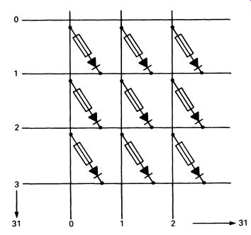
FIG. 9 an array inside a fusible-link EPROM
Where very large numbers of components are required, a manufacturer may specify a special mask to produce the ROM with the program 'built in' at the design stage.
A compromise between the immutable ROM and the volatile RAM has been produced, in the form of the erasable programmable read-only memory (EPROM). The EPROM uses MOSFET technology, and during programming-by the repeated application of pulses of moderate voltage (a few tens of volts)-charges are built up in the insulation below the gate. This layer has an extremely high resistance, and the charge cannot leak away.
The presence of the charge causes the MOSFET to conduct, and the charged cell is read as a 1. EPROMs can retain their data for many years.
It is, however, possible to discharge the cells in the EPROM by exposing it to intense ultraviolet light. The light causes a photoelectric current to flow, conducting the charge away. EPROMs of this type have a transparent window in the encapsulation above the chip, to allow the chip to be illuminated while protecting it from mechanical damage.
QUESTIONS
1. Add the following two binary numbers: 100011 1001
2. What is meant by (i) RAM, (ii) ROM, (iii) EPROM?
3. Convert the following binary number into 2's complement form: 10010101
4. What is the maximum number of addresses possible using twelve address lines?
5. Dynamic RAM is often preferred in personal computer systems; compare dynamic RAM with static RAM. How do the differences affect the user of the computer?