AMAZON multi-meters discounts AMAZON oscilloscope discounts
In digital computers the semiconductor diode has effected dramatic reductions in size, power consumption, failure rate, and temperature rise. In a machine containing 1,500 diodes, for example, the filaments of diode tubes would require a total of 225 watts. The extent of the size reduction may be grasped from the fact that a modern microminiature computer diode takes 1/18,000 or less of the space occupied by a miniature diode tube.
Considerable effort has been exerted to improve diodes for computer use. Some of their electrical parameters which have been refined include switching time, front-to-back resistance ratio, internal capacitance, forward conductance, and maximum operating voltage. This section describes several of the principal applications of diodes in digital computers.
REQUIREMENTS FOR COMPUTER DIODES
The signals in a digital computer are fast pulses which do the counting. Semiconductor diodes used in these machines must have certain closely-held characteristics, otherwise pulses will be lost or extra ones generator-both of which will lead to inaccuracies in computation. Principal among these characteristics are low forward resistance, high back resistance, low self-capacitance, low self-inductance, short reverse recovery time, and extended high-frequency response.
Satisfaction of these requirements has led to the computer diode, a component manufactured especially for digital applications. Computer diodes are available in both germanium and silicon varieties over a wide range of electrical ratings.
Their reliability ratings are superior. Aside from stringent electrical requirements, size also is an important consideration in the computer diode. The reason for this is that a digital computer uses only a very few basic circuits, but these are repeated great numbers of times in the machine. Therefore, components used in these iterative circuits must be as small as practicable if the machine is to be kept reasonable in size.
OR CIRCUIT
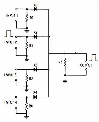
Fig. 7-1. OR circuit.
The OR circuit is the simplest diode logic circuit employed in the digital computer. Fig. 7-1 shows this type of circuit with four inputs against a single output. But the arrangement is not limited to four--the scheme may be repeated endlessly by adding one diode and one resistor for each new input.
The circuit has the property that it will produce a positive output pulse, across common-load resistor R5, if there is a positive pulse at any one of the inputs ; that is, if 1 or 2 or 3 or 4 is energized. The reason for this is that the input pulse forward-biases the diode, and the resulting pulse current develops a pulse voltage drop across R5.
The resistance of input resistors R1-R4 and output resistor R5 will depend on the diode characteristics, output resistance of pulse source, and input resistance of the circuit to be driven by the OR circuit.
AND CIRCUIT
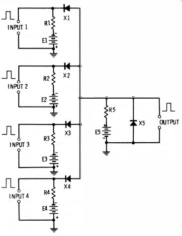
Fig. 7-2. AND circuit.
Fig. 7-2 shows a second type of logic circuit-the AND circuit. Unlike the previous circuit, this one delivers an output pulse only if input 1 and input 2 and input 3 and input 4 are all energized simultaneously. Although four inputs are shown, the scheme may be repeated as required by adding one diode, one resistor, and one DC source for each input, provided the total current can be safely handled by diode X5.
In this circuit, current flows from each DC bias source and the common bias (E5) through the corresponding input resistor and R5 (thus, in section 1, from E1 and E5 in series through R1 and R5). This results from the fact that the diode is forward-biased by the DC voltage. All diodes, input bias voltages (E1-E4) , and input resistors (R1-R4) are identical.
In the absence of simultaneous input signals, diode X5 clamps the output below ground (Fig. 1-12, Section 1) . When a positive pulse of sufficient amplitude is applied to an input, the corresponding diode is cut off ; but this does not produce an output pulse, since current through the other diodes and X5 maintains the clamp. When equal-amplitude pulses are applied to all inputs simultaneously, however, clamping diode X5 is cut off (since X1, X2, X3, and X4 now are cut off, and the X5 current is interrupted), and an output pulse is delivered. Thus, all inputs must be energized at the same time for output to occur.
The values of the input resistances and voltages depend on diode characteristics, input-pulse amplitude, desired output pulse amplitude, and required E5 voltage. Diode X5 must be rated to pass safely the total pulse current of all input sections.
DIODE MATRIX
Information in the form of electrical pulses may be electronically switched rapidly (at rates up to several million per second) from one to another of a large number of paths by means of a diode matrix. Such a matrix is a lattice of conductors (Fig. 7-3) insulated from each other, and in which diodes are connected to form one-way paths between the horizontal and vertical conductors at certain of their intersections.
There are many matrix configurations and many ways of using each of them. In Fig. 7-3, eight horizontal and six vertical paths are shown, but this number may be extended indefinitely in each direction. In this example, the matrix is supplied with DC, and positive-pulse signals are applied to one or all of six pairs of signal-input terminals. There are eight separate outputs, and only one combination of input signals will switch the DC voltage to a given output terminal for the duration of the pulse. The other output terminals will be low-voltage or zero at this time.
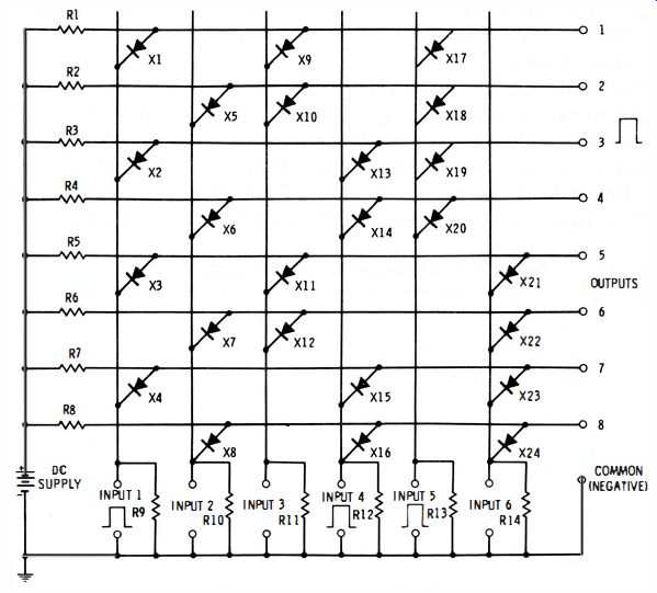
Fig. 7-3. Diode matrix.
This action is accomplished in the following manner : If there were no diodes in the circuit, the DC voltage would appear at all eight output terminals. But the diodes, being forward-connected, ground all the horizontal lines through all the vertical lines to which the diodes are connected. (Thus, horizontal line 4 is grounded to vertical lines 2, 4, and 5 by diodes X6, X14, and X20, respectively. The only voltage that can appear at the output, therefore, is the small voltage drop produced by diode forward current flow through R4-X6-R10 and R4-X20-R13 in parallel, and this can be made nearly zero by selecting R10, R12, or R13 small with respect to R4.) In the initial condition, therefore, all diodes are conducting.
In order for full output voltage to appear at a given output terminal, all diodes connected to the line running to that terminal must be cut off. This is accomplished by applying positive pulses of sufficient amplitude simultaneously at the proper input terminals. Thus, when pulses are applied simultaneously at inputs 1, 4, and 5, as shown in Fig. 7-3, the output pulse appears at terminal 3. Table 7-1 shows the inputs which must be simultaneously energized to produce an output pulse at the terminal shown.
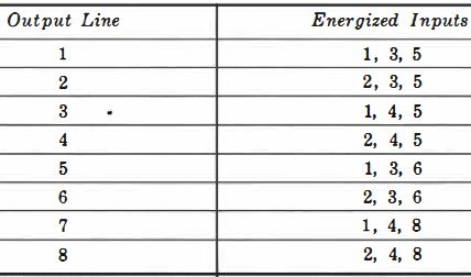
Table 7-1. Diode Matrix Switching Data.
For low-voltage circuitry, such as that employed with transistors, R1-R8 each may be 20,000 ohms, R9-R14 each 500 ohms, all diodes Type 1N800 silicon computer units, supply voltage +9 volts and pulse-signal voltage + 1 volt peak. If the minimum load connected to any of the output terminals is 5,000 ohms, the output signal amplitude will be 1 volt peak.
One use of a diode matrix is to sense the On and Off condition of tubes or transistors in the flip-flops of a counter.
The output pulses activate neon lamp circuitry which indicates the count. In this way, the convenient ten counts of the decimal system may be obtained from a cascade of four flip-flops which are by nature binary (base-2 ) counters.
COUPLING DIODES IN FLIP-FLOPS
Fig. 7-4 shows the use of coupling diodes in flip-flops. Function and action of these diodes is the same in each circuit. Fig. 7-4A shows a tube circuit, and Fig. 7-4B an equivalent transistor circuit.
Coupling diodes serve to transmit the triggering pulse automatically to the tube which is cut off, rather than applying it simultaneously to both tubes and possibly causing missed switching. When VI is On, its plate voltage is reduced by plate current flow through R1. V2 is nonconducting at this time, and its plate voltage is high. When the negative trigger pulse is applied, it passes readily through diode X2 to the plate of V2 and switches that tube on.
In Fig. 7-4B, action is the same except for the use of NPN transistors. For PNP transistors, reverse the polarity of all diodes and the DC supply.
(A) Tube circuit. (B) Transistor circuit.
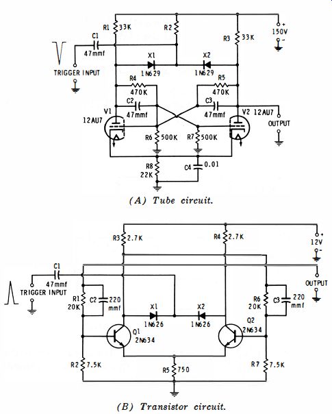
Fig. 7-4. Coupling diodes in flip-flop.
Since the diodes are connected between two plates (or two collectors ), their reverse resistance must be high in order to prevent an extraneous DC path between the tubes or transistors. Silicon diodes possess a natural high reverse resistance.
High-back-voltage germanium computer diodes, such as those shown in Fig. 7-4, also have sufficiently high back resistance when rated at three to four times the plate or collector voltage.
CLAMPING DIODES IN FLIP-FLOPS
As in other circuits, clamping diodes are used in flip-flops to limit the swing of a voltage (in the flip-flop, usually the output-signal voltage). Fig. 7-5 shows the use of clamping diode pairs (X1-X2 and X3-X4) to limit the excursion of the two outputs of a tube-type flip-flop. The same arrangement would be used with a transistor circuit.
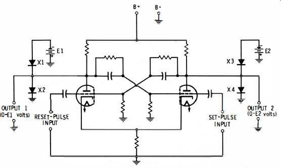
Fig. 7-5. Clamping diodes in flip-flop.
The swing is limited to the voltage established by E1 for output 1 and E2 for output 2 (Fig. 1-12, Section 1).
TUNNEL DIODE FLIP-FLOP
Fig. 7-6 shows a simple bistable (flip-flop ) circuit employing one 1N3712 tunnel diode (X) . This circuit operates with a DC supply of 3 volts at 1.1 ma.
The tunnel diode has two stable states in this circuit ; low voltage high-current, and high-voltage low-current. These correspond respectively to about 55 mv at 0.9 ma, and 250 mv at 0.5 ma.
Initially, the circuit is quiescent in its first state, and approximately 55 mv appear at the output terminals. A 1.5-volt peak positive trigger pulse will switch the circuit to its second state, and approximately 250 mv will appear at the output.
A subsequent lo5-volt peak negative pulse will switch the circuit back to its first (low-output-voltage) state.
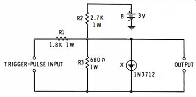
Fig. 7-6. Tunnel diode flip-flop.
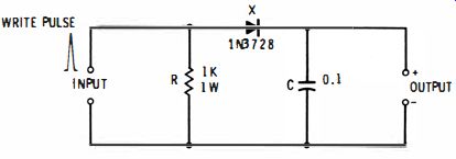
Fig. 7-7. Diode-capacitor memory cell.
DIODE-CAPAC ITOR MEMORY CELL
At slow counting speeds, a charged high-quality capacitor may be used as a memory cell in a computer in which only a few storage elements are required. A silicon diode prevents capacitor discharge back through the writing source.
Fig. 7-7 shows the circuit. A positive Write pulse applied to the Input terminals charges the 0.1-mfd capacitor (C) through the low forward resistance of the 1N3728 silicon diode (X) . The charged voltage of the capacitor will be equal to the peak pulse amplitude less the small forward voltage drop across the diode. This capacitor must have low leakage. When the pulse ceases, the capacitor holds the charge, since it cannot discharge back into the pulse source, because of the extremely high reverse resistance of the diode. This charged voltage may be detected (read ) at the Output terminals as the stored information. The Read circuit should have low resistance, in order to discharge the capacitor.
TUNNEL-DIODE MEMORY CELL
The bistable tunnel-diode circuit shown in Fig. 7-6 may be used as a nondestructive memory cell, in addition to its intended function as a flip-flop.
The positive input pulse is the Write signal, and it switches the output to its high-voltage stable state. This state, representing storage in the memory cell, may then be read repeatedly with a high-resistance circuit (1,000 ohms or more) without destroying the storage. A subsequent negative input pulse acts as an Erase signal, "emptying" the cell by switching the circuit to its low-voltage stable state.
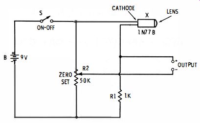
Fig. 7-8 Photodiode card or tape reader.
PHOTODIODE TAPE OR PUNCHED CARD READER
Fig. 7-8 shows a fast-acting photoelectric circuit which may be used for reading punched cards or punched tape. The light-sensitive element is a 1N77B germanium photo diode (X) . This is a tiny unit (0.006-inch in diameter) with a built-in lens in one end.
The diode is connected in a bridge circuit for balancing out its dark current (about 10 microamperes). Adjustment is simple; close switch S, darken the cell, and set potentiometer R2 for zero DC, as read with a DC VTVM connected to the OUTPUT terminals. After the circuit has been zeroed, light intensity of 70 foot-candles will produce an output of 6 volts across a 1-megohm load. The output may be applied to a suitable DC amplifier for boosting in power.
Maximum current drain from the 9-volt supply (B) is 200 microamperes.