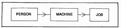
Fig. 3-1. Block diagram of a simple microprocessor operation.
| Home | Audio mag. | Stereo Review mag. | High Fidelity mag. | AE/AA mag. |
For a simple explanation of what is a microprocessor, we can use Fig. 3-1, which shows a person who has a machine that is needed for a task of some sort. If the task is as simple as turning on a light, the person must control the machine (flip a switch). Please note that the control information is all in one direction-from left to right. Also, if the task contains many steps or procedures, the person must remember the entire sequence to perform the operation completely.
Figure 3-2 shows the process of information flow in a micro processor system. Again the microprocessor receives a command from an input device which may or may not be controlled by a person. However, for sequenced operations we take the memory requirement away from the person and transfer it to the memory, which is part of the system. The input command may be only a signal, a pulse, caused by pushing a start button, whereas the output could be a complete series of actions whose codes are stored in memory. These codes are referred to as the program. Determining or setting up these codes is referred to as programming.
What does the microprocessor chip actually do? In reality, it can do anything that the input device or memory tells it to do. To keep this easy to understand, we can divide all the microprocessor activities into two categories:
It routes data output from input or memory to output or memory. This is simply a movement of data from one place to another, somewhat like a large multipole, multiposition switch.
It performs operations on data, operations such as algebraic addition and subtraction, comparison of two numbers, and even some simple logical decision making, such as branching in a flow chart. We can see a micro chip has two sections of circuitry: a control section, which takes care of housekeeping details of data routing; and an arithmetic logic-unit (ALU) to perform the various operations.
Fig. 3-1. Block diagram of a simple microprocessor operation.
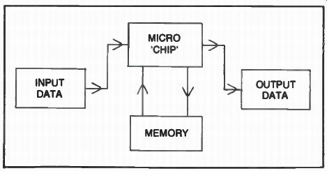
Fig. 3-2. Block diagram of a micro system.
BUSSES
To get information to and from the microprocessor brain or CPU, a system of address, control and data busses are required.
These busses, as they are referred to in computer jargon, are a group of conductors over which bits of data are transferred to and from various points in the system. Some are bidirectional busses, which means that information can be transferred in both directions.
Generally, only one transfer of data can occur at one time for each bus. Some of the more sophisticated systems use a time-sharing or bit-slicing technique which enables more than one data transfer at a time. In addition to microprocessors, many logic designed devices use time-sharing on a single lead wire.
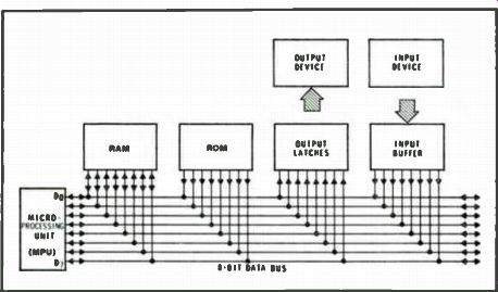
Fig. 3-3. Typical data bus arrangement.
Running the Bus Lines
A digital bus is a path over which digital information is transfer red from any of several sources to any of several destinations. Only one transfer of information can take place at any one time. While such a transfer is taking place, all other sources that are tied to the bus must be disabled. The verb, to bus, means to interconnect several digital devices, which either receive or transmit digital information, by a common set of conducting paths, called a bus, over which all information between such devices is transferred.
The basic purpose of a bus is to minimize the number of interconnections required to transfer information between digital devices. Busses are present within IC chips, such as the 8080A microprocessor; between IC chips as with the address, control, and bidirectional data busses present in the 8080A; and between digital systems and instruments.
The concept of a bus is probably one of the most important concepts in digital electronics. Without the ability to share information paths, most digital devices would require three or four times the number of wire connectors that are now needed. Printed circuit boards for microcomputers would be considerably more complex... and expensive.
Figure 3-3 shows a simple data bus setup for a microcomputer.
In this system all data transfers are via the MPU. Note that data can be moved in either direction between the RAM and the MPU. All other data moves in one direction only. Data can be moved from the ROM or input buffer to the MPU. And data can be sent from the MPU via latches to the outside world.
To fetch and retrieve data transfers properly (in this case, only one at a time) an address bus must be added to the system. Each data source is then assigned a different address. As an example, the RAM, ROM, input buffers, and output latches all have chip enable pins. The correct logic pulse at these pins will activate or enable the circuit. With a different address for each circuit, then only one circuit will function at any given point in time. The address bus is shown in Fig. 3-4, a block diagram of a micro system.
In this micro system, inputs to the address decoders come from the MPU via the address bus. And the outputs go to the chip enable lines of these various circuits. Only one address can appear on the address bus at any one point in time, thereby enabling only one external circuit at a time.
Just as each home has its mailing address, so must each byte have its assigned address. When any one of these addresses appear on the address bus, the RAM is selected via its chip enable line.
Note that part of the address bus connects directly to the RAM, which selects the individual byte within the RAM chip.
ROM is also assigned a range of addresses that must he enabled when any of these addresses appear on the address bus.
The output latch and input buffers are also assigned specific addresses. In this way, the MPU can "talk to" any of the external circuits just by putting the correct address on the address bus.
Fig. 3-4. Addition of the address bus.
There is another problem because of the nature of two-state digital logic circuits. Regardless of which of the two states they are in, the circuits interfere with output of the enable circuit. For example, if the output of the disabled circuits assumes a high state, this will then interfere with a low output of an enabled circuit. Thus, you will have a condition where one circuit tries to pull the bus high while the other one is trying to go low. A tri-state device is usually used in microprocessors to overcome this problem.
TRI-STATE LOGIC
A tri-state logic device has a third state in addition to the logic 1 and logic 0 states. Figure 3-5 illustrates the common noninverting buffer along with the tri-state, noninverting buffer.
The noninverting buffer increases the current drive of the input signal without altering the logic levels. For this reason, the output could drive 10 times as many gates as the input. The common buffer has one input and one output. The output always has the same logic levels as the input. Thus, the input must be either 1 or 0. And the output must follow the same logic.
However, the tri-state buffer has two inputs. Along with the normal data input, the buffer has an enable/disable input. The input can be either a logic 1 or logic 0, depending on whether the buffer is to be enabled or disabled. The tri-state buffer in Fig. 3-5B is enabled by applying logic 1 to the enable/disable input.
This unique tri-state concept allows outputs to be tied together and then connected to a common bus line. Normal TTL outputs cannot be connected because of the low-impedance logical "1" output current which one device would have to sink from the other.
If, however, both the upper and lower output transistors are turned off on all but one of the connected devices, then the one remaining device in the normal low-impedance state will have only a small amount of leakage current to supply to, or sink from, the other devices.
It is true that in a TTL system, open-collector gates could be used to perform the logic functions of these tri-state elements, but neither waveform integrity nor optimum speed would be obtained.
The low-output impedance of tri-state devices provides good capacitance drive capability and rapid transition from the logical "0" to logical "1" level, thus assuring both speed and waveform integrity. It is possible to connect as many as 128 devices to a common bus line and still have adequate drive capability to allow fan-out from the bus.
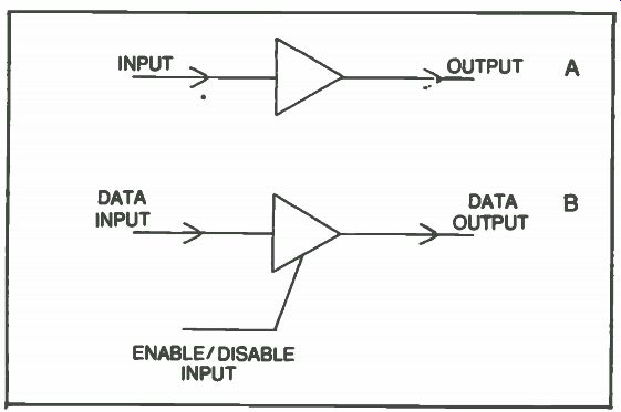
Fig. 3-5. Common noninverting buffer at (A) and tri -state noninverting buffer
at (B).
Another advantage of tri-state buffers is that in the high impedance state, their inputs do not present the normal loading to the driving device. This is significant when it is desirable to transmit in both directions over a common line. In summation, a tri-state device has three possible output states:
A logical "0" state.
A logical "1" state.
A high-impedance output state that is, in effect, disconnected from the bus line.
All three-state devices have an input pin called an enable/ disable input, which permits the logic devices either to behave normally or to exist in the high-impedance state. When enabled, a tri-state device behaves as a normal TTL device. When disabled, a tri-state device behaves as if it is, in effect, disconnected from the circuit.
SIMPLE BUS SYSTEM EXAMPLES
As we look at Fig. 3-6, you will see a simple four-device one-fine bus system that is based upon the use of a single 74126 three-state buffer chip. You can tell this is a bus system since the outputs of gates A through D are connected together. With standard 7400-series TTL chips, you could not use this is a bus system unless the chips have special output circuits-either three-state or open collector-that permit bussing.
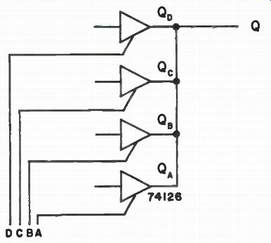
Fig. 3-6. A simple four-device one-line bus based upon the use of four 74126
tri-state buffers.
If we assume that gates A through D in Fig. 3-6 are enabled by a logic "1" input, the operation of the circuit should be clear. Only one buffer gate may be enabled at any instant of time, and the remaining buffer gates must be disabled. Thus, digital information from only one of the four buffers appears on the single-line bus at any given time. Information from the remaining three buffers is blocked because the corresponding buffers are disabled.
Typical bus systems consist of multiline busses, as shown in Fig. 3-7, rather than just single-line busses. Other than the fact that the gating inputs enable or disable four buffer gates at a time, this circuit is identical to that shown in Fig. 3-6 for a one-line bus.
DATA STORAGE
In order to operate and function, a microprocessor or computer must have a program. And this program must be stored in a memory device. Stored in these memory devices are data and complete instruction steps for each of the microprocessors that function. These are addressable memories that send out and receive bit patterns to store and retrieve data in these memory banks.
These instructions are seen by the microprocessor as binary codes in memory and are fetched out in eight-bit (a byte) chunks.
Some types of memories are read-only memory (ROM), read-write memory (RWM) and random-access memory (RAM).
ROM is used to store program steps in dedicated micro systems.
Read-write memory is used to store data that changes during program operations. Random-access memory lets the microprocessor read and write from it and allows data to be stored while the program is in progress. Let's take a more detailed look at these various memory families.
The Read-Only Memory System
In order to run their programs, all micro systems must have read-only memory devices. And usually, dedicated micros will use only ROMs. To refresh your memory, ROM is an acronym for read-only memory. ROM is then a permanent memory and is nonvolatile. Its contents will therefore be unaltered with power loss or system operation error. In most cases ROMs have a random access feature. The micro cannot change the contents in the ROM, but can only read what has been stored.
A typical memory IC contains over 4,000 flip-flops, stored charges, or diodes programmed in an array of 512 x 8 bits. Refer to Fig. 3-8. Each memory cell (a bit) is programmed to yield a logic "1" or "0" output. Each row of 8 bits is called a byte, or can be referred to as a word. When a particular byte is addressed by the micro chip, the memory IC provides eight outputs stored in that byte on eight parallel data lines that are called the data bus.
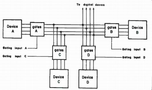
Fig. 3-7. A simple multiline bus arrangement. In this case, there are four
devices and four-line busses.
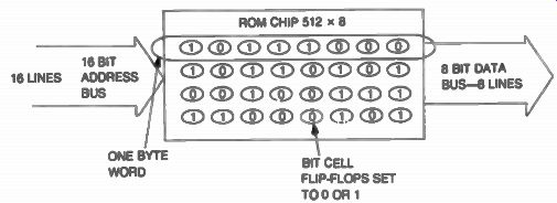
Fig. 3-8. A typical ROM IC. The data information addressed from the ROM IC
chip is fed into the microprocessor to perform a specific task.
The ROM is usually programmed by changing the mask when the IC is fabricated. A PROM (programmable read-only memory) can be programmed by the user before it is inserted into the system. Generally, this type of ROM uses fusible links which can be modified by the user. Then there is the EPROM (erasable PROM), which is also programmed by the user, but can be erased by subjecting it to an ultraviolet light. After erasure, the EPROM can be reprogrammed with a new program if it is removed from the system.
A new INTEL 8355 ROM device with I/O is shown in Fig. 3-9.
The ROM portion is organized as 2048 x 8, or 16,384 bits of memory. It has a maximum access time of 400 microseconds.
The Random-Access Memory System (RAM)
The RAM (random-access memory) is a device into which the micro can write data and from which the micro can read data while it is in the system. This is also referred to as read-write memory.
The RAM is a semiconductor memory into which a logic "0" or logic "1" state can be written (stored) and then read out again or retrieved. Random means that we can access any one of the memory locations by applying the proper logic states to the memory select inputs. Thus, we don't have to sequence through the memory in order to access a memory location. Simply stated, RAM differs from ROM in that the micro can read from and write into it, storing data while the program is operating. Most micro systems will have both ROM and RAM devices. Technically speaking, ROMs can also be called RAMs.
RAMs are divided into two types: static and dynamic. The static RAM stores each bit in a flip-flop stage. The dynamic RAM stores the data as capacitive charges. However, for dynamic RAMs an operator must periodically access these word bits in order to refresh the charges, lest the memory would fade away like an old soldier.
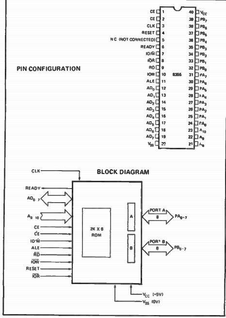
Fig. 3-9. The INTEL 8355, a 16,384-bit ROM with I/O (courtesy of INTEL).
The dynamic RAM can store a lot more data in a given space as compared to a static memory. The dynamic RAM is much faster than the static one and consumes less power for each state change.
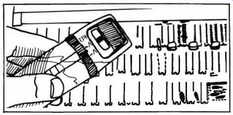
Fig. 3-10. A technician checking a RAM board with a digital voltmeter.
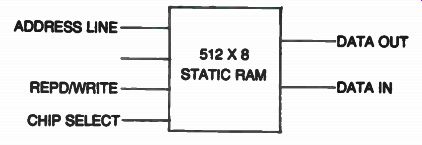
Fig. 3-11. Static RAM input and output lines.
However, additional refresh circuitry is required for a dynamic RAM, and for many chips this is out-boarded. The term refresh, or renew, means to sequence among several states so rapidly that the digital circuit memory cannot detect that the states are being sequenced. Refresh implies that the same information is applied to each state, respectively, on every sequence cycle. Refresh is required so that data stored in the RAM will not be lost.
Figure 3-10 shows a technician checking a RAM board with a digital voltmeter. This is a 16K RAM memory board that plugs into a S-100 bus that is used in a SOL-20 microcomputer system built by Processor Technology Corp.
Static RAM Control Lines. Refer to Fig. 3-11. Several control lines are required for a static RAM, and they include:
• Data out--This is a single line to output a certain bit to be addressed.
• Data in--A single line is used to input the particular bit to be placed in memory.
• Address lines--The number of address lines depends on the size of the RAM. A 1024-bit RAM needs 10 address lines.
• Read-write--This is a single line with which the command to read (output) or write (input) is fed to the microprocessors.
• Chip select or enable--Again a single line is used to disconnect the memory from the output data bus, to inhibit the WRITE circuitry in the chip and to control accessing of the chip.
Dynamic RAM Control Lines. Refer to Fig. 3-12. The control lines required for a dynamic RAM chip are the following:
--Data out lines--The number of these lines required depends on RAM chip storage word size.
-- Data lines in--The number of these lines required depends on word size in the RAM chip.
-- Address lines--The number of address lines required depends on the number of words the RAM can store.
-- Chip selects or enable--This line is used to control input and output from the memory. One pulse on this line is required for each READ or WRITE cycle.
-- Read-Write--The command to READ (output) or WRITE (input) is given over this line. The line is usually held in the READ state.
--Precharge-This line must be pulsed before the output line is read so as to charge the output capacitors. This pulse timing in relation to chip select pulse is critical.
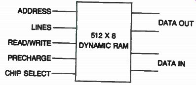
Fig. 3-12. Dynamic RAM input and output lines.
Static MOS RAM
One of the storage units for a MOS-type static RAM is shown in Fig. 3-13. Many of these units are in a typical MOS RAM, along with bus drivers and address decoders. The storage unit contains six MOS transistors. These N-channel devices can be made to conduct by feeding a positive voltage to the gate terminal: there fore, when the gate is close to ground potential, the transistor is off and has a very high impedance. Now, when the gate goes high the transistor conducts and has a good bit lower impedance. By this action "1" and "0" are stored in these units.
INTEL's 5101 family of static CMOS RAMs is shown in Fig. 3-14. These RAMs use fully DC stable (static) circuitry, and it is not necessary to pulse the chip select for each address transition. The data is read out nondestructively and has the same polarity as the input data. The 5101 has separate data input and data output terminals. An output disable function is provided so that the data inputs and outputs may be WIRE-OR-ed for use in common data I/O systems.
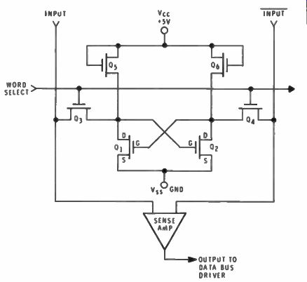
Fig. 3-13. MOS static RAM storage unit.
Fig. 3-14. INTEL's 5101 IC is a 256 x 4-bit static RAM (courtesy of INTEL).
Fig. 3-15. A pulse train generated by the clock.
THE CLOCK AND ITS OPERATION
The clock is the heart of most logic devices, because it moves the system in an orderly fashion and keeps all logic pulses in step or synchronized. This is referred to as step-by-step or sequential logic systems. These sequential operations are controlled with a pulse signal from the clock. The clock device generates a precise pattern of 0's and 1's (pulse train), as illustrated in Fig. 3-15. The time of one complete clock cycle is called a period. The frequency of the clock is the reciprocal of the period. Astable multivibrators, such as the 555 IC timer shown in Fig. 3-16, operate at several megahertz are used to produce these clocking pulses. A crystal-controlled astable circuit is desired for microprocessor applications.
With the clocked-logic system, when an input condition changes, the output will not respond immediately, but waits until the arrival of the clock command. When this occurs, the output logic then responds. For this reason, then, clocked logic does not run wild, but steps through all program changes in an orderly manner.
With logic step action counters, latches, shift registers, printers and various memory devices can now be utilized. Thus, every change occurs in steps with clocked logic which greatly reduces glitches and timing sequence mix-ups. The prime logic devices used with the clocked system are latches and various flip-flops.
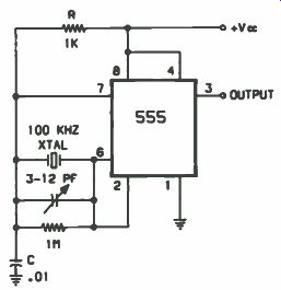
Fig. 3-16. An astable multivibrator clock circuit. This one is crystal controlled.
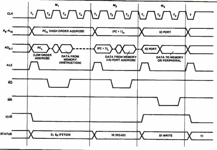
Fig. 3-17 Complex digital pulse waveforms tor the INTEL 8085 microprocessor
(courtesy of INTEL).
A bistable device is just another name for a flip-flop. This is a circuit in which the output has two stable states (output states 0 and 1) and can be caused to go into either of these states by an input signal. The circuit remains in that state permanently after the input signal is removed. Thus, a flip-flop is a device having two stable states with the capability of changing from one state to another with the application of a control signal, and remaining in that state after the signal has passed.
POSITIVE AND NEGATIVE EDGES
A digital scope waveform is a graphical representation of digital pulses that shows the variations in logic states as a function of time.
This is usually referred to as the systems timing diagram.
The digital waveforms make it possible to show the logic conditions that exist at a certain point in time of a complex digital circuit. The digital circuit need not be complex, but the use of digital waveforms is essential for complex circuits. For simple logic circuits, the digital waveforms might need to show only one or two points in the logic circuit. For complex circuits, 10 or more digital waveforms may be needed to help you understand the various functions. An example of a complex train of pulses is shown in Fig. 3-17, this one for the basic timing of INTEL's 8085 microprocessor.
For any digital waveform, the time progresses from left to right.
The lower state, or baseline, of a digital waveform is usually considered to be the logic 0 state. The top portion of the pulse is the logic 1 state, or greater than +2.5 volts. You may assume that the change from a logic 0 state to a logic 1 state, which is called a positive edge, occurs almost instantaneously (in several nanoseconds or less). This change is represented by the vertical "step-up-line" in Fig. 3-18.
The old adage of "what goes up must come down" also applies to pulses. The drawing in Fig. 3-19 illustrates the change from a logic 1 to logic 0 by the vertical step-down line that is called the negative pulse edge.
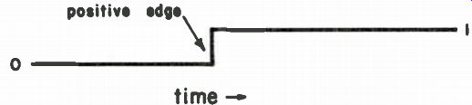
Fig. 3-18. A positive pulse edge.
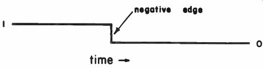
Fig. 3-19. A negative pulse edge.
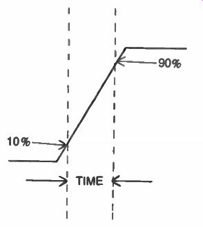
Fig. 3-20. Pulse rise time.
RISE AND FALL TIME
It does appear-even on a fast scope--that the change occurs instantaneously, but it does not. With these state changes, there is both a rise time and a fall time.
The rise time is the time required for the positive leading edge of a pulse to rise from 10 percent to 90 percent of its final value. You will find that it is proportional to the time constant and is a measure of the steepness of the pulse wavefront. In digital electronics, rise time is the measured length of time required for an output voltage of a digital circuit to change from a low voltage level (logic 0) to a high voltage level (logic 1). The pulse rise-time phenomenon, shown in Fig. 3-20, should illustrate this to you more clearly.
Fall time is the time required for the trailing edge of a logic signal pulse to decrease from 90 percent to 10 percent of its initial value. In digital electronics, fall time is the measured length of time required for an output voltage of a digital circuit to change from a high voltage level (logic 1) to a low voltage level (logic 0).
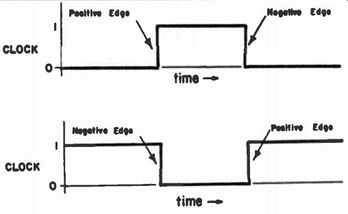
Fig. 3-21. Positive and negative clock pulse edges.
PROPAGATION DELAY
While thinking of rise and fall time, it would now be appropriate to discuss propagation delay as it pertains to pulse signal travel throughout digital/logic systems. Propagation delay is a measure of the time required for a logic pulse signal to travel through a logic device or series of logic devices forming a logic string. This delay also includes all of the interconnecting signal pulse lead paths between IC chips on the PC boards. It occurs as the result of four types of circuit delays: storage, rise, fall and turn-delay. This is the time between when the input signal crosses the threshold-voltage point and when the responding output voltage crosses the same voltage point. The propagation time varies from different types of TTL gates. A low-power TTL gate chip has a propagation delay of as much as 33 ns, whereas a Schottky TTL chip has a propagation delay of only 3 ns. When you are working with very high digital frequencies and complex logic circuits, the concept of propagation delay can be quite important. Always keep this in mind, then, when troubleshooting these logic devices. Even when you may be bread boarding digital chips and testing them at low frequencies, the concept of propagation delay could be important and cannot be disregarded.
CLOCK AND TRIGGER PULSES
The 7490 decade counter is one type of many various digital electronic devices that contain flip-flops and change state upon the application of a clock pulse. When working with these flip-flops it is important to keep in mind which edge of a clock pulse the logic transition state occurs. Thus, whether it is a positive or negative edge transition must be considered when troubleshooting these devices. Figure 3-21 illustrates these positive- and negative-going clock pulses with the designated positive and negative pulse edges.
An edge-triggered flip-flop is one type of flip-flop in which some minimum clock signal rate of change, in volts/second, is a necessary condition for an output change to occur. And a trigger pulse is a pulse that starts the action in a flip-flop or other digital device. It may well be the positive or negative edges of the trigger pulses that start this action.
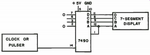
Fig. 3-22. Block diagram of the 7490 decade counter.
DIGITAL WAVEFORMS AND TIMING
A digital waveform is a graphical representation of a digital signal, showing the variations in logic state as a function of time. In a complex digital circuit, you need many different waveforms, corresponding to different points in the digital circuit, in order to understand the behavior of the circuit as a function of time.
To better understand this logic operation, we will start with the 7490 decade counter shown in Fig. 3-22. Note that the clock input is fed in at pin 14. A series of digital waveforms for the 7490 decade counter is shown in Fig. 3-23. The specific waveform points in the circuit and figure are as follows:
• The A clock input is at pin 14 of the 7490 chip.
• The A output is at pin 12 on the 7490 chip.
• The B output is at pin 9 on the 7490 chip.
• The C output is at pin 8 on the 7490 chip.
• The D output is at pin 11 on the 7490 chip.
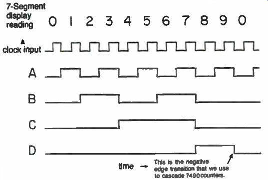
Fig. 3-23. Series of digital waveforms for the 7490 decade counter.
Let's now consider the transition from 3 to 4 on the seven segment display. When the display is at 3, the four outputs of the 7490 counter have the following logic states:
A = 1
B = 1
C = 0
D = 0
These logic states correspond to the 4-bit binary-coded decimal (BCD) word 0011, which corresponds to 3 on the display. Now observe what happens on the negative edge of the clock pulse between 3 and 4. We see that both A and B return to logic 0 and C goes to logic 1. The new BCD output from the counter is 0100, which corresponds to 4 on the display.
Another important transition is from 9 to 0 on the seven segment display. This transition occurs at the negative edge of the single clock pulse at output D. For every 10 full clock pulses input at the A clock input pin, there is a single output clock pulse at output D. This is the reason for calling the 7490 decade counter a divide-by ten counter.
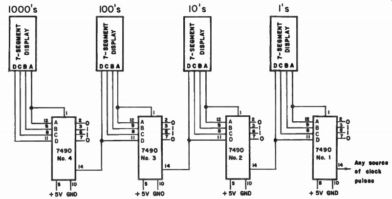
Fig. 3-24. Four cascaded 7490 decade counters, each of which is connected
to its own seven-segment LED display. This circuit can count from 0000 to 9999.
THE 7490 DECADE COUNTERS
To cascade means to arrange two or more similar digital circuits or integrated circuit chips in a way that the output of one circuit or chip provides the input of the next one. This cascading process can continue for as many decades as required. Note the four cascaded decade counters shown in Fig. 3-24. The diagram is arranged so that the most significant digit-the 1000's digit-is on the far left, and the least significant digit, the 1's digit is on the far right. Such a circuit permits you to count clock pulses from 0000 to 9999. Tapping off the four D outputs from the counters will provide divide-by ten, divide-by-hundred, divide-by-thousand and divide-by-ten thousand outputs.