Fig. 4-1. Waveforms found in a divide-by-two circuit.
| Home | Audio mag. | Stereo Review mag. | High Fidelity mag. | AE/AA mag. |
A very obvious and yet most useful feature of two or more trace oscilloscope is they have the capability for viewing two or more waveforms simultaneously that are frequency or phase related, or that have a common synchronizing voltage, such as in digital/logic circuitry. Simultaneous viewing of cause-and-effect waveforms is an invaluable aid to the circuit designer or technician.
FREQUENCY DIVIDER WAVEFORMS
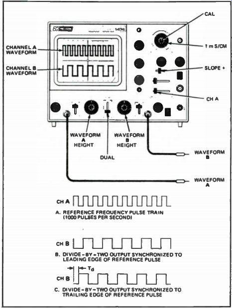
The waveform illustrated in Fig. 4-1 is found in a basic divide by-two circuit. The channel A waveform is the clock pulse train reference. References B and C indicate the possible outputs of the divide-by-two circuitry. Also indicated in Fig. 4- 1 are the settings of specific oscilloscope controls for viewing these waveforms. In addition to these basic control settings, the TRIGGER LEVEL control, as well as the channel A and channel B VERTICAL POSITION controls should be set as required to produce viewable patterns.
Figure 4-1 indicates waveform levels of 2 cm. If the exact voltage amplitude of the channel A and B waveforms are desired, the channel A and B VARIABLE controls must be placed in the CAL position. The control adjustments are for a B&K model 1471B dual-trace scope, such as the one shown in Fig. 4-2. The channel B waveform may be either of the ones indicated in B or C. In C, the divide-by-two output waveform is shown for the case where the output circuitry responds to a negative-going waveform. In this case, the output waveform is shifted with respect to the leading edge of the reference pulse by a time interval corresponding to the pulse width.
Fig. 4-1. Waveforms found in a divide-by-two circuit.
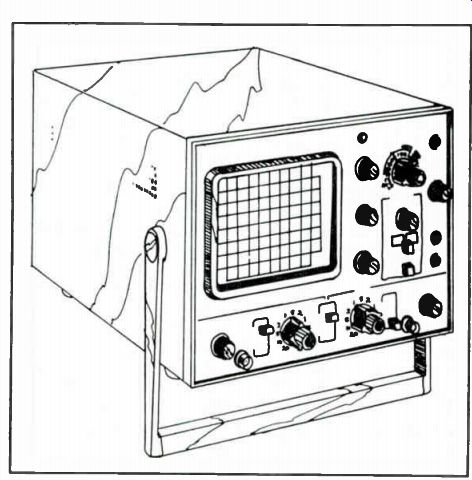
Fig. 4-2. B & K model 1471 B dual-trace oscilloscope.
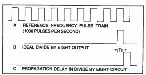
Fig. 4-3. Waveforms found in a divide-by-eight circuit.
DIVIDE-BY-EIGHT CIRCUIT WAVEFORM
The waveform of Fig. 4-3 indicates the relationship for a basic divide-by-eight circuit. You need only to use the basic oscilloscope settings to view these waveforms. The reference frequency of Fig. 4-3A is fed to the channel A input, and the divide-by-eight output is fed to the channel B input. The B waveform reference indicates the ideal time relationship between the input pulse and the output pulse.
In an application where the logic circuitry is operating at or near its maximum design frequency, the accumulated rise time effects of the consecutive stages produce a built-in time propagation delay which can be significant in a critical circuit and must be compensated for. Figure 4-3 indicates the possible time delay that can be introduced into a frequency divider circuit. By using a dual-trace oscilloscope, the input and output waveforms can be superimposed to determine the exact amount of propagation delay that occurs.
PROPAGATION TIME MEASUREMENT
In the preceding paragraph we looked at propagation delay in a divide-by-eight circuit. Significant propagation delay may occur in any circuit with several consecutive stages. A scope, such as the B&K model 1474, has features which allow for simplified measurements of propagation delay. Figure 4-4 shows the resultant waveforms when the dual-trace presentation is combined into a single-trace presentation by selecting the ADD position of the MODE switch. With the channel B polarity switch in the NORM position, the two inputs are algebraically added in a single-trace display. Similarly, in the invert position the two inputs are algebraically subtracted. Either position provides a precise display of the propagation time (Tp). By using the calibrated time measurement, propagation time can be calculated. A more precise measurement can be obtained if the T 9 portion of the waveform is expanded horizontally. Use the HORIZONTAL SWEEP (5x) EXPANSION control for this purpose. It might also be possible to view the desired portion of the waveform at a faster time base speed.
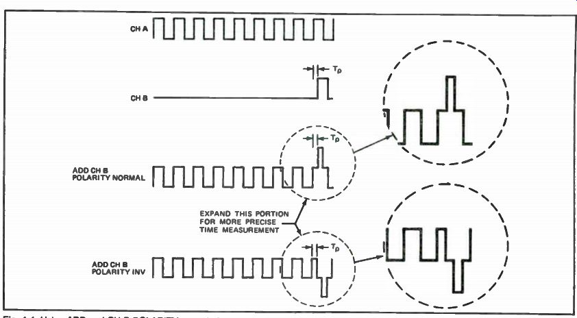
Fig. 4-4. Using ADD and CH B POLARITY controls for propagation time measurement.
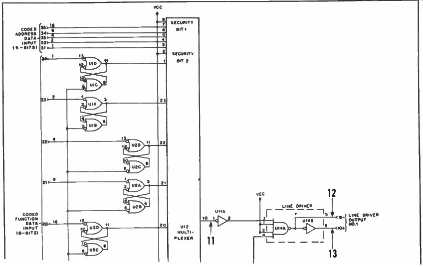
Fig. 4-5. Typical digital circuit using several time-related waveforms.
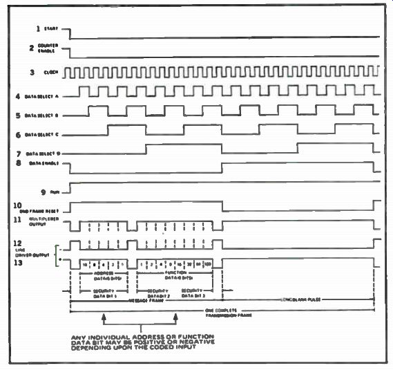
Fig. 4-6. A family of time-related digital waveforms.
DIGITAL CIRCUIT TIME RELATIONSHIP
A dual-trace oscilloscope is a necessity in designing, building and troubleshooting digital equipment. A dual-trace scope permits easy comparison of time relationships between two waveforms.
In digital devices it is common for a large number of circuits to be synchronized, or to have a specific time relationship to each other. Many of the circuits are frequency dividers that have just been described, but many waveforms are often time-related in many other combinations. In the dynamic state, some of the waveforms change, depending upon the input or mode of operation.
Figure 4-5 shows a typical digital circuit and identifies several of the points at which waveform measurements are appropriate. Figure 4-6 shows the normal waveforms to be expected at each of these points. Their timing relationships to one or more of the other waveforms are known to be correct. The dual-trace oscilloscope allows this comparison to be made. For scoping this system, waveform 3 would be displayed on channel A and waveforms 4 through 8, and 10, would be successively displayed on channel B, although other timing comparisons might be desired. Waveforms 11 through 13 would probably be viewed on channel B, and waveforms 8 or 4 would be viewed on channel A of the oscilloscope.
In the family of time-related waveforms shown in Fig. 4-6, waveform 8 or 10 may be used as the sync source for viewing all of the waveforms, because there is only one triggering pulse per frame. You can also switch the scope to external sync by using waveform 8 or 10 as the sync source. With external sync, any of the waveforms are viewable without readjustment of the sync controls.
Waveforms 4 through 7 should not be used as the sync source because they do not contain a triggering pulse at the start of the frame. In most cases, it would not be necessary to view the entire waveforms as shown in Fig. 4-6. In fact, there are many times when a clear examination of a portion of the waveforms is appropriate. In such cases, it is recommended that the sync remain unchanged while time-base speed or x 5 magnification be used to expand the pulse waveform display. A four-channel scope, such as the Philips PM 3214 shown in Fig. 4-7, will let you view a family of time-related waveforms found in microprocessor circuits more accurately and easily.
CLOCK OR PULSE GENERATION
Microprocessor systems and most all digital/logic devices re quire some type of clock pulse in order to perform and time the various functions. The clock generates accurately timed pulses and may be crystal controlled. The logic systems are gated or enabled by these clock pulses. The faster the clock frequency, the more functions that can be performed, but this speed is limited by response time of the ICs used in the system. Clocks vary from simple local devices to the very diverse and complex systems.
The simple clock puts out equally spaced pulses and should be as narrow as possible and still enable the gates. The reason for the narrow clock pulses is to discriminate against noise pulses or glitches. Some systems require a two-phase clock, such as the 8080A microprocessor IC that we will look at shortly.
Thus, the clock is the very heart of most digital/logic systems.
For this reason then, the clock pulses should be one of the first items to be checked with the scope when troubleshooting these systems.
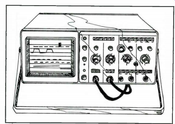
Fig. 4-7. Philips model 3214 four-channel oscilloscope used for digital troubleshooting.
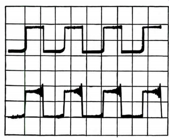
Fig 4-8. Pulse distortion when the probe shield is not grounded.
One note of caution when using a scope probe for observing these clock pulses. If the shielded probe case of the oscilloscope is not properly grounded, erroneous clock pulse waveforms on the scope might trick you into seeing a distorted pulse when there is none. Not only should the ground lead from the scope case be connected to the chassis ground of the equipment under test, but the ground shield of the probe must be connected to the ground pin of the clock IC you are testing. This caution is readily illustrated for a clock pulse shown in the bottom trace of Fig. 4-8 where the probe shield was not grounded. Note the ringing distortion on the pulse waveforms. A clean clock pulse is shown in the top trace of the figure with the probe shield properly grounded. Always use an x10 attenuation scope probe for checking clock and logic pulses. These clock pulses can radiate, or transmit, very potent radio frequency signals (if the complete unit is not properly shielded and I/O lines filtered) and can cause interference in other nearby electronic devices. Thus, if you have some strange acting equipment problems, be on the alert for this type of rf spectrum pollution.
Clock Inputs for the 8080A
An 8080A microprocessor chip requires a two-phase clock pulse input. A clock in digital/logic jargon is a device that generates at least one clock pulse, or a timing device that provides a continuous series of timing pulses. A two-phase clock is a two input timing device that provides two continuous series of timing pulses that are synchronized together with a single clock pulse from the second series always following a single clock pulse from the first series. Figure 4-9 shows the timing of these two clock pulses. The top trace is the phase 1, and the bottom trace is the phase 2 clock pulse.
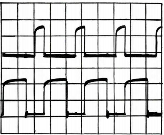
Fig. 4-9. Timing of the 8080A two-phase clock pulses.
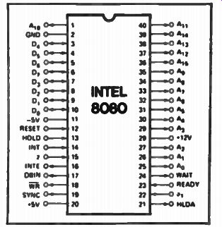
Fig. 4-10. 8080A pinout diagram.
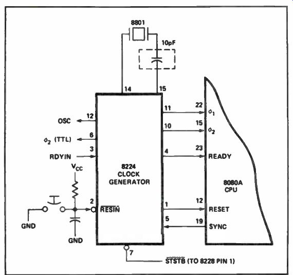
Fig. 4-11. 8224 clock block diagram.
It is stated in the 8080A specifications that the minimum pulse width for clock phase 1 is 60 ns, and the phase 2 clock pulse width is 220 ns. Refer to Fig. 4-10 for the pinouts of the INTEL 8080A chip.
This is a two-phase non-overlapping clock system. These clock pulses can be generated with an INTEL 8224 clock generator chip.
Clock Frequency Check with a Counter
A frequency counter is now an essential instrument for checking out digital/logic, microprocessor, PLL and other divider systems now found in almost all electronic devices encountered by the electronics service technician. Your first step for isolating problems in a nonoperational logic system is to check for clock operation and correct clock frequency. The frequency counter is used to check the output from the clock generator chip. If you were troubleshooting a system that uses the popular 8080A microprocessor, these two check points would be pins 10 and 11 of the 8224 clock generator chip shown in pinout and block diagram of Fig. 4-11. The 8080A requires two phase clock signals at pins 15 and 22. This clock generator IC also requires a crystal for accurate frequency generation and control.
Loop Pickup Counter Measurements
There may be cases where you cannot make direct connections to the clock input signal or do not want to because of circuit loading. The probe capacitance of the frequency counter could cause the frequency of the oscillator to change, or stop the clock oscillator from running in a worst-case condition. The pickup loop (shown near the clock crystal in Fig. 4-12) allows signals to be picked up without a direct probe connection. For this application, the inductive loop is used to pick off the frequency pulses quickly, without any direct connections. This action eliminates any interference with the measured circuit. You may not obtain an accurate count of the clock pulses because the input signal to the frequency counter from the pickup loop will be a sawtooth or sinewave shape because of coil induction. The pickup loop can also be connected to the input of the scope to take a quick look at various oscillator signals.
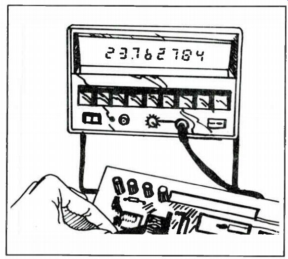
Fig. 4-12. Frequency counter with a pick-up loop being used.
Inductive Pickup Loop Applications
For these tests we are using the Sencore model FC51 1-GHz frequency counter and rf pickup loop. Select the desired input, read rate and frequency range. Place the pickup loop near a capacitor or coil in the oscillator circuit to be tested. If an unstable count is obtained, reposition the pickup loop in order to stabilize the count. If no count is obtained, turn over the pickup loop (which reverses the polarity of the pickup loops coil), or select a different component in the circuit.
The pick-up loop will work best when placed next to or around a coil. However, a high-sensitivity counter will let you pickup signals from capacitors, transistors, ICs or crystals in most circuits.
Most clocks in digital/logic systems use a clock to keep the frequency pulses stable and accurate. Should the clock not operate or be off frequency, the crystal would be the prime component suspect. To check this crystal is an easy task to perform if you have a Sencore FC51 frequency counter. The crystal check feature on this instrument allows any crystal with a fundamental frequency of 1 to 20 MHz to be checked. Note in Fig. 4-13 that a crystal is inserted in the front panel universal crystal socket to check for crystal activity. The crystal will be made to resonate at its fundamental operating frequency.
CRYSTAL CHECK PROCEDURE
Use the following procedure to check a crystal with the Sencore FC51 frequency counter. First, insert the crystal to be tested into the front panel crystal check socket. Select the desired READ RATE button. Depress the 20-kHz to 100-kHz FREQUENCY RANGE button. Depress the CRYSTAL CHECK button. Read the fundamental crystal frequency on the digital LED readout of the counter.
The crystal check reads the approximate fundamental frequency of the crystal under test. Defective or inoperative crystals will be indicated by an intermittent or zero counter readout.
Fig. 4-13. Crystal check on a Sencore FC51 frequency counter.
POWER SUPPLIES FOR LOGIC SYSTEMS
A proper DC voltage power source is required for operation of the microprocessor and logic systems that have been discussed in this guide. In fact, all digital/logic systems must have very precise regulated DC power supplies that are well filtered. Use your scope to check for a smooth DC output voltage from the power supply and check for correct regulated DC voltage levels to all logic circuits with a DVM. Most of these voltage supplies are electronically regulated and filtered.
The scope can be used to monitor the DC supply lines in order to catch spikes in TTL (transistor-transistor logic) systems as the gates function and filters or bypass capacitors may have opened up.
Thus, a very fast, wide-band triggered-sweep scope is required to detect these transient pulses.
When a TTL circuit is switched from a low to a high state, transients occur on the supply voltage line because of the TTL totem pole output action. Note the typical TTL gate circuit shown in Fig. 4-14. When the logic level goes high, it is actually short circuiting the supply voltage during a brief period.
If several gates switch on simultaneously, the current spike on the supply line is increased linearly with the number of gates. These spikes or glitches, which are caused by insufficient DC supply line filtering, can trigger on fast TTL gates and be quite fatal. By fatal we mean to destroy information stored in memory systems (PROMs, ROMs, RAMs, etc.). So use your scope to check those DC voltage power-supply lines for open filter or bypass capacitors.
To track down these spikes or glitches in a microprocessor system, you not only need to check at the DC power-supply voltage output terminals, but at various filter or bypass points throughout the system. You will notice that there are many filter and bypass capacitors located throughout any logic device that contains many gates. The logic pulse scope trace shown in Fig. 4-15 is of a properly operating gate. Should a filter capacitor become open in this stage, a scope pulse like that shown in Fig. 4-16 may well develop. Note the small spikes as the pulse goes from a high to a low transition. The amplitude of these spikes will vary as to which filter capacitor C1 or C2, is faulty, in the case of the TTL gate circuit shown in Fig. 4-14.
If you use the scope to check the DC-regulated voltage coming out of the logic system power supply, you should see a smooth, clean trace, such as shown in the top trace of Fig. 4-17. This is true even with a very high vertical scope AMPLIFIER GAIN setting.
Should trouble occur in the electronically regulated DC circuit or filter capacitors, some hash or pulses that are shown in the bottom scope trace of Fig. 4-17 will show up.
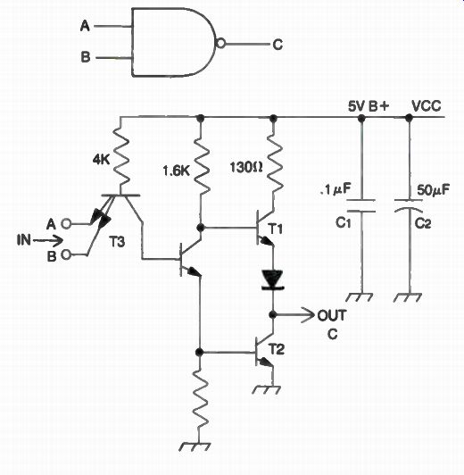
Fig. 4-14. Typical TTL gate circuit.
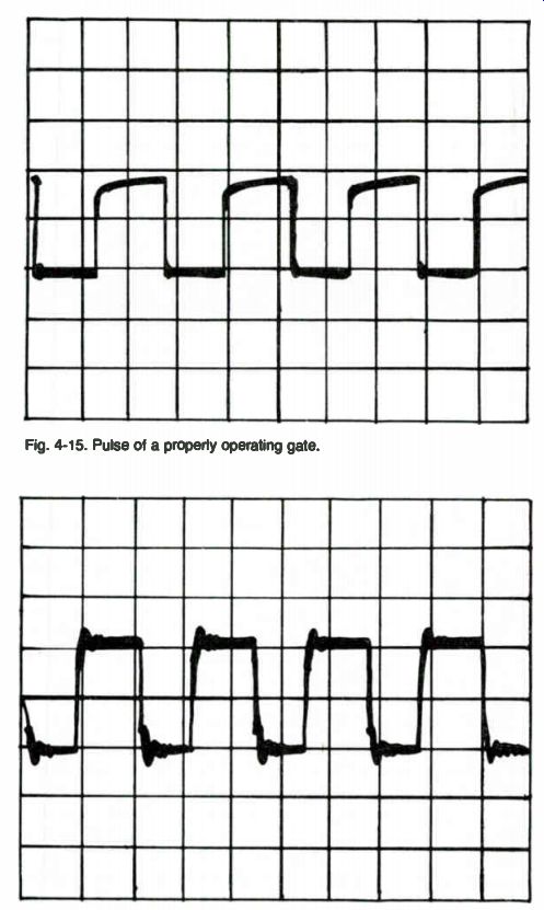
Fig. 4-15. Pulse of a properly operating gate.
Fig. 4-16. Distorted pulse caused by an open filter capacitor.
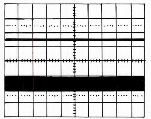
Fig. 4-17. The top trace indicates proper filtering, and the bottom trace
hash shows a poor filtering system.
MICROCOMPUTER POWER SUPPLY
A well .regulated power supply for a microcomputer system is shown in the block diagram of Fig. 4-18. Note that it produces a regulated +5 volts at 3 amps and a +12 volts and -12 volts at .5 amp which supplies all computer operations. This power supply is found in the Processor Technology model SOL-20 minicomputer system. To accurately measure these critical DC voltages that must be supplied to logic devices, a digital voltmeter is an ideal instrument for troubleshooting logic circuits of all types.
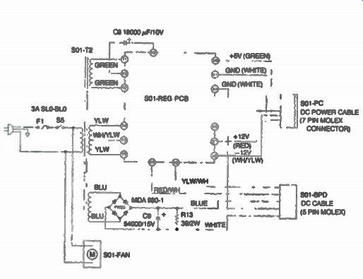
Fig. 4-18. Block diagram of the SOL-20 power supply.
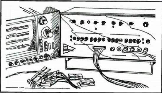
Fig. 4-19. Lab Science VLA-1000 setup.
LAB SCIENCE VLA-1000 LOGIC ANALYZER
The Lab Science VLA-1000 shown in Fig. 4-19 is a general purpose logic analyzer designed for logic designers and troubleshooters. The VLA-1000 probes, selects and records up to 16 parallel digital inputs simultaneously. It stores and arranges this data in one of four possible output formats, and then displays this data on an ordinary X-Y oscilloscope.
The VLA-1000 analyzer has been specifically designed to operate with most scopes that have a horizontal input. Even AC coupled scopes, if their bandwidth is at least from 10 Hz to 100 kHz, will present an excellent display in all modes. The oscilloscope should be capable of full-screen deflection for ±2 volts DC input to both horizontal and vertical amplifiers, and should have input impedances of 100K ohm or greater. Even the lowest price, general purpose scopes can meet these specs. The dual-trace DIA output mode requires a dual-trace scope, but you can observe each byte separately on a single-trace scope and obtain the same information.
Fig. 4-20. DATA domain.
Procedure and Operation
To prepare the VLA-1000 logic analyzer for operation, connect the VLA-1000 to the oscilloscope and set up the VLA-1000 front panel switches as follows:
• Set all PATTERN RECOGNITION WORD switches to X.
• Set DELAY: EVENTS/CLOCKS to CLOCKS.
• Set NORM/DELAY/LOAD DELAY to NORM.
• Set REPETITIVE/SINGLE to SINGLE.
• Set POS/MID/NEG to POS.
• Set DATA DOMAIN/WAVESHAPE/MAP MODE to DATA DOMAIN.
Switch the ON/POWER AC line switch to ON. Now you should see presented on the scope 256 1's and 0's, as in Fig. 4-20. Adjust the intensity, focus, vertical and horizontal gain and positioning of the scope to give a viewable display. To check WAVESHAPE mode, set the DATA DOMAIN/WAVESHAPE/MAP MODE switch to WAVESHAPE. This should give a display similar to that in Fig. 4-21. To check MAP MODE, set the DATA DOMAIN/ WAVESHAPE/MAP MODE switch to MAP MODE. This display will probably not look like the MAP MODE shown in Fig. 4-22, but will most likely be just a few dots near either the upper left or upper right of the scope screen (location 0000 16). This is because the VLA-1000 memory has come up loaded with mostly zeros. If the cluster of dots is in the upper left corner, change to the opposite polarity HORIZ + jack on the VLA-1000 panel, and use only that polarity for this scope.
Fig. 4-21. Waveshape mode.
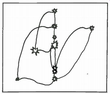
Fig. 4-22. Map mode.
Fig. 4-23. Dual-trace D/A upper and lower bytes.
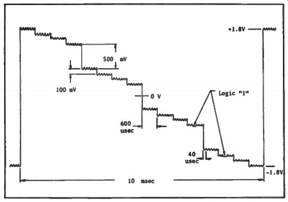
Fig. 4-24. Horizontal output with data domain.
Fig. 4-25. Vertical output with data domain.
To check the DUAL-TRACE D, A mode, set up the scope for externally triggered horizontal sweep operation. Now set the horizontal sweep speed to 1 ms/division, connect the VLA-1000 DISPLAY SYNC output jack to the external trigger input of the oscilloscope, and connect the selected (from the previous step) + HORIZ output jack to the second vertical input channel of the scope. Set both VERTICAL CHANNEL SENSITIVITIES to 2 V/division.
This display will probably not look much like the one shown in Fig. 4-23, because the memory is loaded with mostly zeros. It does, however, represent the same data as the other three display modes.
To illustrate a more common use of the EVENTS DELAY capability, set the REPETITIVE/SINGLE switch to SINGLE. Disconnect the clock from the test circuit so it will stop counting. Next, momentarily depress the RESET switch to the VLA-1000. Reconnect the clock to the test circuit allowing it to resume counting. The VLA-1000 will pass over the first three occurrences of the all-zero pattern recognition word and then record and display the data desired indefinitely until restarted by either depressing the RESET switch or switching the REPETITIVE/SINGLE switch back to REPETITIVE. This feature allows the logic designer or troubleshooter to examine data at practically any time slot window of its sequential states. The VLA-1000 has no provision for delaying on both clocks and events in the same operation, but the POS/MID/ NEG control does provide the user the capability to observe data 15 clocks either before or after the desired delay number of events.
Output Waveforms
Figures 4-24 through 4-27 show the waveforms of the VLA 1000 for the VERT and HORIZ outputs indicated, in data domain and waveshape modes, with voltage levels and timing indicated. For individual units, these may vary - ± - 20 percent from those shown.
Theory of Operation
The VLA-1000 block diagram, shown in Fig. 4-28, illustrates the functional groups of the instrument. For clarity, all details have not been shown.
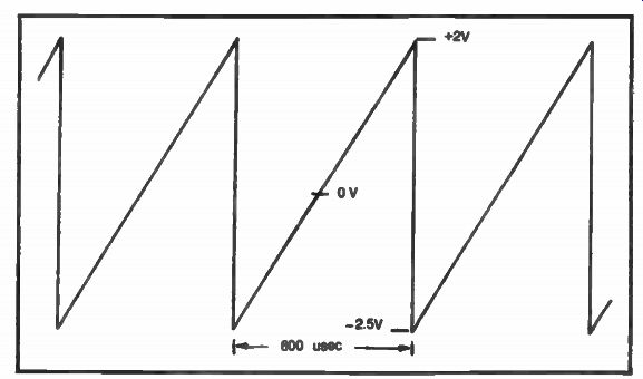
Fig. 4-26. Horizontal output with waveshape mode.
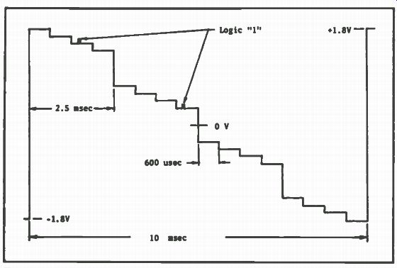
Fig. 4-27. Vertical output with waveshape mode.
Theory of Operation
The purpose of a logic analyzer is to selectively record and display data from a complex digital electronic circuit and present it on the screen of an oscilloscope in an easily recognizable format.
The VLA-1000 accomplishes this task by recording 16 data inputs, strobed by an externally supplied synchronous clock, until a selected pattern recognition word is recognized, and then presenting this digital word along with 15 adjacent words in one of four possible display formats: data domain, waveshape, map mode, or dual trace D/A. At the upper left of the block diagram, 16 data lines enter the instrument, are buffered, inverted and conditioned to TTL levels and then clocked into a 16-bit, 1-word storage register to produce 32 terms for input to the PATTERN RECOGNITION switches as well as to the 16-bit x 16-word static RAM memory.
The address lines of this memory are driven by a four-stage real word binary counter. An identical four-stage pseudo-word binary counter shares a common clock but is preset by the timing and control logic to accommodate the POS/MID/NEG display arrangement selected by the user. This operation can be seen in the VLA-1000 control logic flow chart shown in Fig. 4-29.
The carry bit from the pseudo-word counter clocks a four-stage bit counter, which drives the address lines of a one-of-six data selector, which produces the 256 bits of stored memory serially, one bit per 40 U sec. This serial data bit line drives an analog gate to produce 1's and 0's as required in the data domain mode, and the LSB of a vertical D/A converter in waveshape mode. Two 8-bit data selectors steer data and position information into the two D/A converters (vertical and horizontal) to present data, as required, for the selected output mode. A ramp generator provides horizontal sweeps for waveshape mode, and a quadrature oscillator provides sine and cosine waveforms for data domain mode. The D/A converters are driven directly by the memory MS byte and LS byte, respectively, in map mode and dual-trace D/A mode.
A 16-bit DELAY COUNT STORAGE REGISTER is loaded by depressing the LOAD switch on the panel. This stored word controls the count down of the 16-bit bcd counter for events or clocks delay (up to 9999) from the selected pattern recognition word.
MICROPROCESSOR APPLICATIONS
In the following diagrams, Figs. 4-30 through 4-33, you will find timing and CPU pinout data and selective store clock-qualifying in formation for some microprocessors in use today. This information is intended as only a guide to the user and should be used as such.
Most microprocessors have different timing characteristics depending upon the instruction being executed: fetch, execute, I/O, DMA, etc. Therefore, the timing diagram and clock-qualifying circuit shown might not display the desired address bus or data information. In general, address information is available during longer portions of an instruction cycle than is valid data. For this reason, it is best to first locate the sequential address information "window" desired, and then refine the choice of a data clock to present the controlling address bits, substituting data bus inputs for the un changing or "don't care" address bits, up to the maximum capacity of 16 input data lines of the VLA-1000. Another point to remember is that tri-stated or floated inputs can only be represented in the display as 1's or 0's (usually 1's). This display can sometimes be confusing, especially when the user insists on explaining every bit in a truth table or map mode display.
Also, although the CPU pinout is given for each microprocessor, it is far better to trace each signal through the circuit to find a buffered equivalent signal, in order to improve noise immunity and isolation from the processor. Another caution: Many second-source suppliers do not use the exact timing relationships that the particular, original manufacturer does. For this reason, it is best to use the specific CPU manufacturer's data sheets.
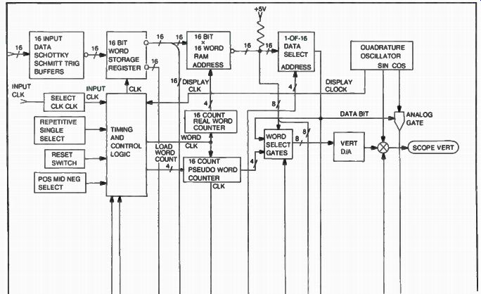
Fig. 4-28. VLA-1000 block diagram.
The selective store clock-qualification schematics shown for some of the microprocessors provide a means to observe only qualified data. This is necessary when address and data buses are time-multiplexed to provide clocking-in of only valid data. Continuous use of the VLA-1000 tied to a microprocessor development system should yield a much broader understanding of the detailed system operation and an insight into design optimization.
SPIKE OR GLITCH LOCATOR
Here is a trick with the triggered-sweep scope that may help you locate an intermittent spike or pulse that at times may be found riding on the regulated DC voltage supplies in digital/logic systems.
For this testing technique, you will need a scope that has a single sweep mode or a one-shot sweep mode. This feature will usually be found on a scope with a delaying time base or an A-delayed-by-B time base generator.
The reason for using this technique is that these spikes are very narrow-usually only 10 or 20 ns long-which makes them difficult to see even on a wide-band (30- to 50-MHz) scope. Also, they are usually random in nature. With this setup, you can use the ready light, which shows the one-shot has been armed, for indicating when a spike has occurred, even if you are not looking at the scope screen. Thus, the scope becomes an automatic glitch monitor.
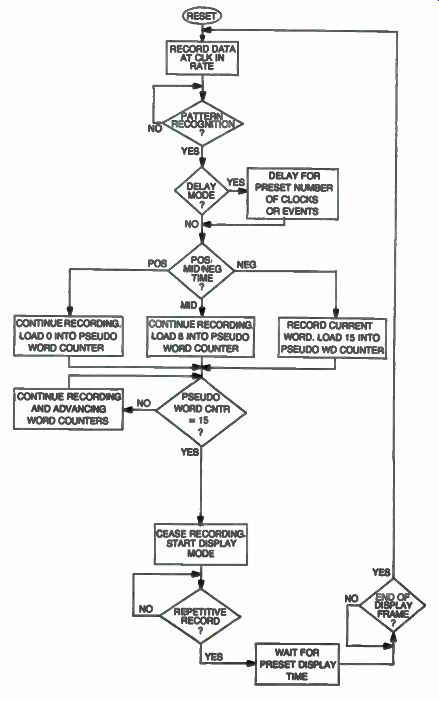
Fig. 4-29. VLA-1000 control logic flowchart.
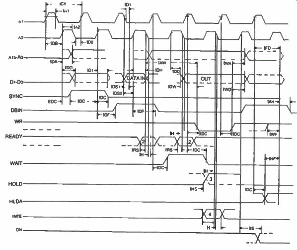
Fig. 4-30. The INTEL 8080A microprocessor (courtesy of INTEL).
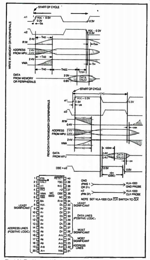

Fig. 4-31. The Motorola MC 6800 microprocessor (courtesy of Motorola).
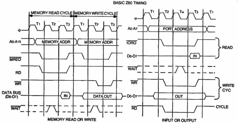
Fig. 4-32. The ZIGLO Z-80 microprocessor.
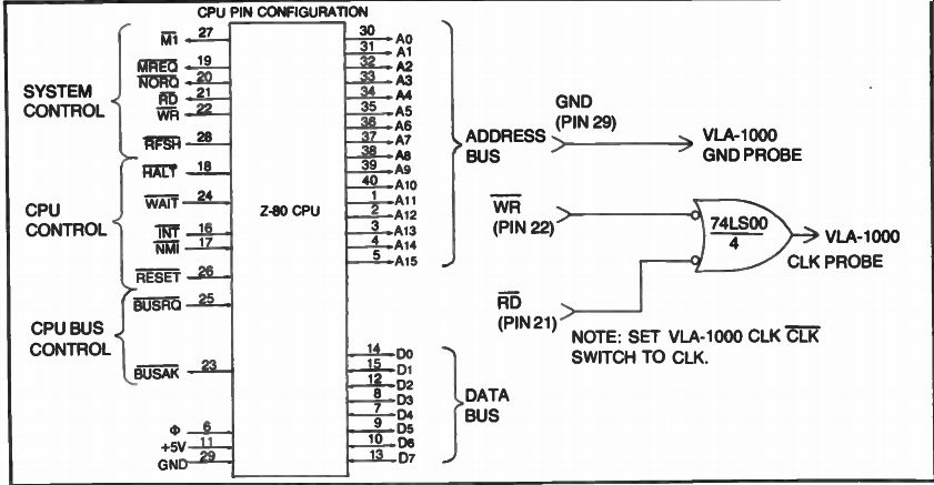
Fig. 4-32. The ZIGLO Z-80 microprocessor (continued).
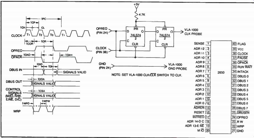
Fig. 4-33. The Signetics 2650 microprocessor.
Fig. 4-34. Oscilloscope panel showing locations of the SINGLE-SWEEP button
and ready light.
Fig. 4-35. Oscilloscope panel showing DELAYED-SWEEP and TIME BASE GENERATOR
controls.
Set up the scope as follows to catch or see an intermittent spike that may occur on the regulated DC voltage power-supply lines.
Obviously, this technique cannot be used on circuit lines that normally carry pulse signals. To activate the one-shot mode, depress the SINGLE SWEEP button as shown in Fig. 4-34. When a spike is detected in the vertical amplifier, the sweep will be triggered on for one single trace, and the ready light will go off. Punch the SINGLE SWEEP button again and the ready light will come back on, indicating that the sweep has been armed again. What we are doing is using the ready light as a visual monitor indicator to determine when a spike has occurred in the circuit under test. Consequently, you do not have to watch constantly the scope screen and can do other service work on the bench. Also, although the spike may be so narrow that you cannot see it on the scope, there be an indication of some action when the single-sweep mode has been fired.
You may have to try various time base generator settings- negative or positive slope (sync) and vertical amplifier gain levels- in order to obtain the spike that will trigger on the single-sweep trace. Some scopes will have a TRIGGER LEVEL control that may need to be varied. The CRT INTENSITY control level should also be adjusted for a bright trace, because there will only be one sweep across the screen. Thus, the one shot sweep enables you to know a spike has occurred that you might not normally be able to see on the scope trace.
Fig. 4-36 Pulses seen with normal scope operation.
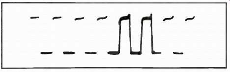
Fig. 4-37. Brighter pulses are A intensified.
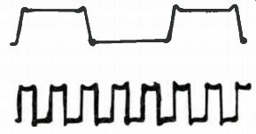
Fig. 4-38. The top trace is produced when the B DELAYED SWEEP button is depressed.
DELAYED-SWEEP SCOPE TRACE
Most triggered-sweep oscilloscopes that have a single-sweep feature (one shot) also have delayed-sweep functions. The controls, shown in Fig. 4-35, include A and B TIME BASE GENERATOR, A MAIN SWEEP, A-INTENSIFIED-BY-B, B DELAYED-SWEEP and DELAY TIME controls. The A and B delayed-sweep modes can be used to look at digital logic pulses and any other complex waveforms that you must observe in greater detail. This delayed sweep will stretch out digital pulses and VIT signals located in the TV video vertical interval blanking bar much better than a X10 expander mode.
We will now use some square wave pulses to see how the delayed-sweep control setting operate. The scope trace in Fig. 4-36 is a normal pulse as you would see it using the "A" time base generator. Now the trace in Fig. 4-37 was obtained by pushing the A-INTENSIFIED-BY-B TIME BASE GENERATOR button. Note that the two pulses are much brighter than the other pulses. These, of course, are the ones that are intensified. You may now rotate the DELAY TIME control and the brightened portion will move smoothly across the display screen. The brightened portion represents the delayed sweep and occurs according to the SEC/DIV. switch setting. The delayed-sweep speed is independent of the main sweep speed, and may be set to any speed equal to or faster than the main A time base sweep generator.
Now press the B DELAYED-SWEEP button and make sure that the intensified portion of the triggered waveform is now displayed across the entire scope screen as in Fig. 4-38. When using the delayed-sweep mode, another feature is that the trace does not have any jitter that usually occurs when you use the x10 magnification mode on single time base oscilloscopes.