Using Logic Probes for Digital Circuit Troubleshooting [Troubleshooting Microprocessors & Digital
Logic (1980)]
When troubleshooting circuits with analog devices, you need only test resistance,
capacitance, or the turn-on voltages of components with two or three states.
The total circuit may be quite complex, but each component in the circuit performs
a simple task and its operation can be easily checked out. As shown in Fig.
5-1, each resistor, capacitor, diode and transistor can be tested by using
a signal generator, VTVM, diode checker, or scope by performing the conventional
troubleshooting techniques. With integrated circuits, however, these various
components cannot be tested. Instead, it is necessary to troubleshoot the total
circuit system.
The difference between discrete circuitry and today's digital ICs is the complexity
of functions performed by these sophisticated devices. Unlike discrete devices,
modern digital ICs perform complete and complex functions. Instead of observing
simple characteristics, it is necessary to observe complex digital signals
and decide if these signals are correct.
Verifying proper component operation now requires observing many inputs-note
the 10 inputs of Fig. 5-1-while simultaneously observing 2 or more outputs.
Thus, another difference between circuitry built from discrete components and
digital IC's is the number of inputs and outputs for each component and the
need to check each one simultaneously.
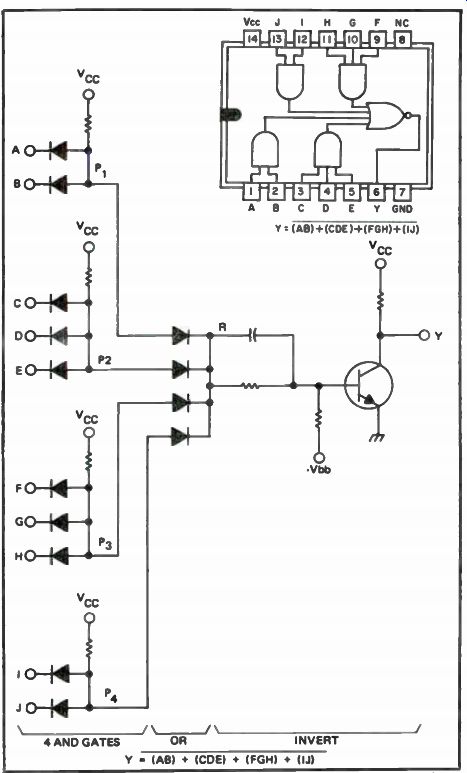
Fig. 5-1. Discrete versus integrated circuits. Troubleshooting circuits built
from discrete components requires verifying relatively simple characteristics
such as resistance, capacitance, or turn-on voltages. Today's circuits built
from digital ICs require the verification of complex digital waveforms defined
by the truth table of the IC.
In addition to simulating test signals and complexity of functions at the
component level, these ICs have caused a new degree of complexity at the circuit
level. If you have enough time, these circuits can be studied and their operations
understood, but the technician just cannot spend that much time. Without going
into all of the intricate operations of the circuit, it becomes necessary to
have a technique for quickly testing each component rather than trying to isolate
a failure to a particular circuit and testing for the expected signals.
In order to solve these problems and to make troubleshooting of digital circuits
more efficient, it is necessary to take advantage of the digital nature of
the signals involved. Tests and techniques designed to troubleshoot analog
circuits do not take advantage of the digital signal and is less effective
when used to troubleshoot digital circuits.
TTL LOGIC SIGNAL
A typical TTL pulse signal is shown in Fig. 5-2. This could well be any analog
signal when viewed on an oscilloscope. The scope displays absolute voltage
with respect to time. For digital pulses, however, absolute values are not
important. A digital signal exists in one of two or three states-high, low,
and an undefined or in between level-each determined by a threshold voltage.
It is the relative value of the signal voltage with respect to these thresholds
that determines the state of the digital signal. And this digital state determines
IC gate operation, not absolute levels. Note in Fig. 5-3 that if the signal
is more than 2.4 volts, it is a high state. For a low state, the voltage must
be below 0.8 volts. It is not important what the absolute level is as long
as it is below this threshold. Therefore, when using the scope, you must always
determine if the signal meets the threshold requirement for the desired digital
state.
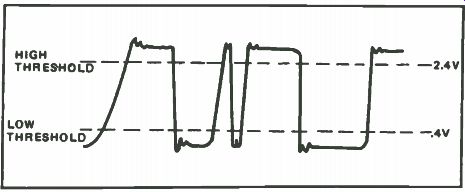
Fig. 5-2. Typical TTL pulse signal. In the digital world, the relative value
of a signal voltage with respect to the threshold determines the operation
of the circuit. A signal above the high threshold is in the high state. Whether
the signal is 2.8V or 3.0V is unimportant to the operation of the circuit.
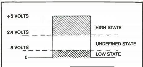
Fig. 5-3. TTL logic levels. 0 to 0.8 VDC is considered to be TTL low state.
2.4 to 5 VDC is considered to be TTL high state.
Each gate in a TTL logic family has a certain propagation delay time, rise
time and fall time. The effects of these timing circuit operations are taken
into account by the design engineer. Timing parameters rarely degrade or become
marginal, so scope checks of these timing parameters contribute very little
to the troubleshooting process.
The circuit in Fig. 5-4 illustrates a problem created by the TTL logic family.
This is a TTL transistor totem pole device. In either the high or low state,
it has a low impedance. In the low state, it appears as about 5 or 10 ohms
to ground. This presents a problem for in-circuit stimulation. A device used
to inject a pulse at a node that is driven by a TTL output must have sufficient
power to override the low-impedance output state. Many pulsers used for troubleshooting
do not have this capability, and the troubleshooter either has to cut the printed
circuit runs or pull IC leads to pulse the circuit under test. These techniques
are time-consuming and can damage other circuits.
A scope and traditional signal sources are inefficient for this reason. Since
the diodes and transistors are packaged in the IC, use of diode checkers are
also marginal. With the complexity of today's electronic circuits, it makes
sense to find the most efficient solution to this problem. The oscilloscope,
diode checkers and voltmeters should be used on analog circuits where they
really shine and use instruments that take advantage of the digital nature
of signals when checking digital circuitry.
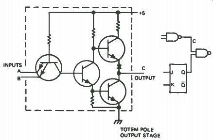
Fig. 5-4. To "jog" this gate, you must override the low-impedance
totem pole output stage.
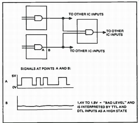
Fig. 5-5. The effect of an open output bond upon circuit operation. An open
output bond allows all inputs driven by that output to float to a bad level.
This level is usually interpreted as a logic high state by the inputs. Thus
the inputs driven by an open output bond will respond as though a static logic
high signal was applied.
WAYS THAT ICs MAY FAIL
To troubleshoot ICs, it is important to know what types of faults are found
in these digital circuits. They can be placed into two main classes-those caused
by internal IC faults and those caused by a circuit failure external to the
IC chip.
There are four types of failures that can occur internally to an IC:
• an open bond on either an input or output
• a short between an input or output and Vcc or ground
• a short between two pins
• a failure in the internal circuitry (often called the steering circuitry)
of the IC.
In addition to these four failures inside an IC, there are four faults that
can occur in the circuit external to the IC:
• a short between a node and a Vcc or ground
• a short between two nodes
• an open signal path
• a failure of an analog component.
Let's now look at the effects these IC faults will have upon circuit operation.
First, the failure for an open bond on either the input or output. In the case
of an open output bond (Fig. 5-5), the inputs driven by that output are left
to float. In TTL and DTL (diode transistor logic) circuits, a floating input
rises to about 1.4 to 1.5 volts and usually has the same effect on circuit
operation as a high logic level. Thus, an open output bond will cause all inputs
driven by that output to float to a bad level since 1.5 volts is less than
the high threshold level of 2.0 volts and greater than the low threshold level
of 0.4 volts. In TTL and DTL, a floating input is seen as a high level.
The effect will be that these inputs will respond to this bad level as though
it were a static high signal.
With an open input bond (Fig. 5-6), you will find that the open circuit blocks
the signal that drives the input from entering the IC chip. The input on the
chip is thus allowed to float and will respond as though it were a static high
signal. It is important to realize that because the open occurs on the input
inside the IC, the digital signal driving this input will be unaffected by
the open and will be detect able when looking at the input pin, such as at
point A in Fig. 5-7. The effect will be to block this signal inside the IC
and the resulting IC operation will be as though the input were a static high.
A short between an input or output and Vcc or ground holds all signal lines
connected to that input output either high (in the case of a short to Vcc)
or low (if shorted to ground), as shown in Fig. 5-8. In many cases, this will
cause expected signal activity at points beyond the short to disappear, which
is catastrophic in terms of circuit operation.
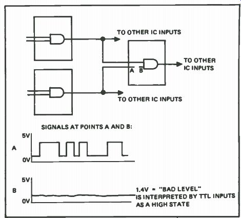
Fig. 5-6. The effect of an open input bond upon circuit operation. An open
bond on an input has the effect of blocking the input signal from reaching
the chip and allows the input of the chip to float to a bad level. Thus even
though the signal can be viewed at an external point such as point A, the input
of the chip responds to the bad level as though it were a static high level.
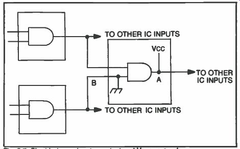
Fig. 5-7. Short between input or output and Vcc or ground.
A short between two pins is not as easy to analyze as a short to Vc, or ground.
When two pins are shorted, the outputs driving those pins oppose each other
when one attempts to pull the pins high while the other wants to pull them
low as shown in Fig. 5-9. In this situation, the output that is attempting
to go high will feed through the upper saturated transistor of its totem pole
output stage while the output trying to go low will sink this current through
the saturated lower transistor of its totem pole output stage. The net effect
is that the short will be pulled to a low state by the saturated transistor
to ground. Whenever both outputs attempt to go high or go low simultaneously,
the shorted pins will respond properly.
Whenever one output attempts to go low, though, the short will be constrained
to be low.
The fourth internal failure of an IC is the steering circuitry within the
IC, as shown in Fig. 5-9. This always causes the upper transistor of the output
totem pole to turn on-locking the output in the high state-or the lower transistor
of the totem pole to turn on-locking the output to the low state. This failure
blocks the signal flow and has a catastrophic effect upon circuit operation.
A short between a node and a Vcc or ground external to the IC or a short internal
to the IC will appear the same. Both will cause the signal lines connected
to the node to be either always high (for shorts to Vcc) or always low (for
shorts to ground). When this type of failure is encountered only a very close "eye
ball" examination of the circuit will reveal if the short is external
to the IC. An open signal path in the circuit has an effect similar to an open
output bond driving the node, as shown in Fig. 5-10. All outputs to the right
of the open will be allowed to float to a bad level and will appear as a static
high level in circuit operation. Those inputs to the left of the open will
be unaffected by the open and will respond as expected.
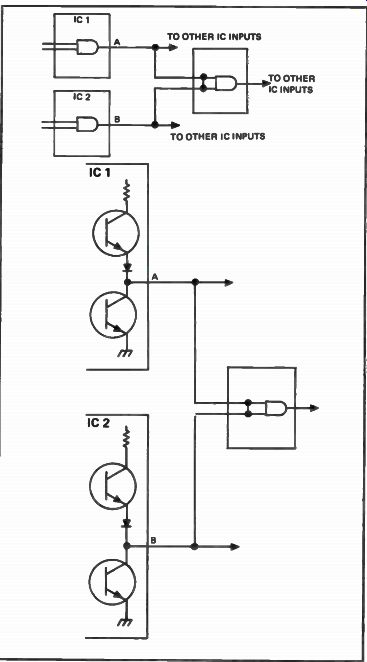
Fig. 5-8. Effect of a short between two pins of an IC.
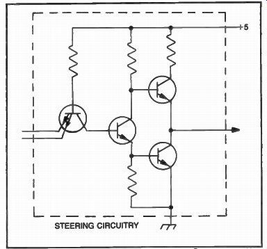
Fig. 5-9. Failure of an internal steering circuit within an IC.
THE MODEL DP-50 B & K LOGIC PROBE
The B & K digital probe is designed for fast analysis of digital circuits
and is compatible with TTL, DTL, RTL, CMOS, MOS and other solid-state circuitry.
Three LED indicators at the probe tip display pulse presence high and high
1 and low 0 logic states. An incorrect logic level or an open pin is indicated
by the absence of a lighted pulse LED. Two switches allow you to select TTL
or CMOS logic thresholds and pulse stretch mode or memory modes. In the pulse
stretch mode, short duration pulses are stretched for a clear visual indication.
In the memory mode, a single digital pulse causes a LED to remain lighted until
reset. This permits you to freeze the display of digital action. The B & K
DP-50 is shown in Fig. 5-11.
Threshold Level Operation
Set the THRESHOLD switch to the TTL position to
select the correct threshold level for TTL, DTL, etc. Use the CMOS position
for MOS and CMOS digital circuits.
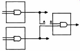
Fig. 5-10. Effect of an open circuit external to an IC.
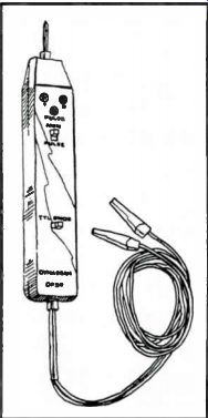
Fig. 5-11. B & K model DP-50 logic probe.
Mode Selection
The MODE switch provides pulse detection in either pulse stretch (PULSE position)
or memory (MEM position) modes. In the pulse stretch mode the PULSE indicator
lights a minimum of 200 milliseconds in response to each single pulse of 20
nanoseconds or greater duration. If the input pulse is short, it is stretched
to 200 milliseconds to assure a high-visibility flash on the LED. In the memory
mode, the PULSE indicator remains lighted after the first pulse or logic transition
until it is reset by moving the mode switch to the PULSE position. To use the
memory mode, set the MODE switch to the PULSE position and then connect the
probe tip to the point being checked. This initial contact will cause the pulse
indicator to flash. Following the initial flash, move the MODE switch to the
MEM position. The probe is now ready to operate in the memory mode.
Using the Probe
The 1 indicator will remain lighted only during the time period when logic
level 1 is present at the probe tip. Similarly, the 0 indicator will remain
lighted only during the time period when the logic level 0 is present at the
probe tip. The PULSE indicator will light as the result of a transition in
logic levels. Thus, typical operating situations may be encountered as follows:
• With the probe tip touching symmetrical pulses, the 0 and 1 indicators
will both be lighted at one-half brilliance, and the PULSE indicator will be
lighted at full brilliance.
• With the probe tip touching a positive-going, high-speed pulse of a short
duty cycle, the 0 and PULSE indicators will be lighted, and the 1 indicator
will be partially lighted on duty cycles greater than 10 percent.
• With the probe tip touching negative-going, high-speed pulses of a short
duty cycle, the 1 and PULSE indicators will be lighted. The 0 indicator will
be partially lighted on duty cycles that are greater than 10 percent.
• When only the PULSE indicator is illuminated, system noise or pulses above
50 MHz are indicated.
• With the probe touching an open pin or an incorrect logic level (a voltage
within the deadband), indicator will light.
LOGIC PROBES BY CONTINENTAL SPECIALTIES
The logic probe, like the Continental Specialties (now Global Specialties
Corporation) LP-1 shown in Fig. 5-12, detects, memorizes and displays logic
levels, pulses and voltage transients in mixed and single logic family systems.
It detects out-of-tolerance logic signals, open-circuit nodes, as well as transient
events down to 50 nanoseconds while providing the user with an instant easily
interpreted high-intensity LED readout.
The probe tip of the LP-1 is connected to a dual-threshold window comparator
and bipolar edge detector. The window comparator bias network sets the LOGIC "1" and
LOGIC "0" threshold levels. The levels are fixed in the DTL/TTL mode
(2.25 volts and 0.8 volts) in the CMOS/HTL mode.
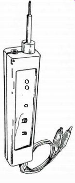
Fig. 5-12. Continental Specialties LP-1 logic probe.
The bipolar edge detector responds to both positive and negative transitions
and drives a pulse stretcher circuit. The pulse stretcher converts level transitions
as well as narrow pulses to one-third of a second in length that drive one
of the three readout LEDs. In the memory mode, the output of the edge detector
is fed to a latching flip-flop.
Using The Logic Probe
Connect the clip leads of the logic probe to the power
supply of the circuit under test. Then set the LOGIC FAMILY switch to DTL/TTL
or CMOS/HTL and the MEMORY/PULSE switch to the PULSE position. Touch the
probe tip to the circuit node to be analyzed. The three display LEDs on the
probe body will instantly provide a reading of the signal activity at the node.
The memory mode of the LP-1 is used to detect, store and display low-repetition
rate or single-shot pulses as well as transient events, even when an observer
is not around when they occur.
A chart for interpreting the action of the logic probe LEDs is shown in Fig.
5-13. The relation of probe tip voltage to probe power supply voltage is shown
in the Fig. 5-14.
---------------
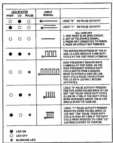
Fig. 5-13. Chart for interpreting the LED readouts of the probes.
LOGIC "0" NO PULSE ACTIVITY LOGIC "1" NO PULSE ACTIVITY
ALL LEOS OFF
1. TEST POINT IS AN OPEN CIRCUIT.
2. OUT OF TOLERANCE SIGNAL.
3. PROBE NOT CONNECTED TO POWER.
4. NODE OR CIRCUIT NOT POWERED.
THE SHARED BRIGHTNESS OF THE HI AND LO LEDS INDICATE A 50% DUTY CYCLE AT THE
TEST POINT.K1OOKHz1 HIGH FREQUENCY SQUARE WAVE 1> 100KHz 1 AT TEST NODE.
AS THE HIGH FREQUENCY SIGNALS DUTY SHIFTS FROM A SQUARE AVE TO EITHER A HIGH
OR LOW WAVE DUTY CYCLE PULSE TRAIN EITHER THE LO OR HI LED WILL BECOME ACTIVATED.
LOGIC "0" PULSE ACTIVITY PRESENT POSITIVE GOING PULSES SINCE HI LED
NOT "ON" PULSE TRAIN DUTY CYCLE IS LOW RE <15%. IF THE DUTY CYCLE
WERE INCREASED ABOVE 15% HI LED WOULD START TO TURN ON. LOGIC "1" PULSE
ACTIVITY PRESENT NEGATIVE GOING PULSES, SINCE LO LED NOT "ON" PULSE
TRAIN DUTY CYCLE IS HIGH RE >85% IF THE DUTY CYCLE WERE REDUCED TO <85% "LO" LEO
WOULD START TO TURN ON.
------------
Powering Up The Probe
The LP-1 is protected against excessive voltage and reverse voltage on its
power leads. Connect the black lead to the common (-) and the red clip lead
to plus (+) Vcc. In order to minimize the possibility of power supply spikes
or other spurious signals from affecting the operation of the probe, connect
the power leads as close to the node to be tested as possible.
Memory/Pulse Switch - Pulse Position
Each time the input signal changes state, the pulse LED is activated for 0.3
seconds. When observing low-frequency, low duty cycle signals, the pulse LED
provides a quick indication of the pulse activity at the node under test. By
observing the HI and LO LEDs, the phase of the pulse train can be determined.
If the HI LED is on, the signal is normally high and pulsing low, and so on.
High-frequency signals cause the pulse LED to flash at a 3-Hz rate.
Memory/Pulse Switch - Memory Position
The LP-1 probe contains a pulse memory flip-flop that catches and holds (memorizes)
level transitions or pulses as narrow as 50 nanoseconds. The memory is activated
by either positive or negative level transitions.
To set the probe for catching and memorizing an event, just touch the probe
tip to the node under test with the switch in the MEMORY position. The next
event that occurs will activate the pulse LED and latch it on. To reset and
rearm the memory, move the MEM/PULSE switch to the PULSE position and then
return it to the MEM position.
NOTE: When arming the memory, the probe tip must be in contact with the test
point in question. If the memory is armed with the tip floating (not connected),
the memory will be activated when the tip makes contact, thus yielding a false
readout.
Fig. 5-14. Voltage relation chart for the LP-1 logic probe.
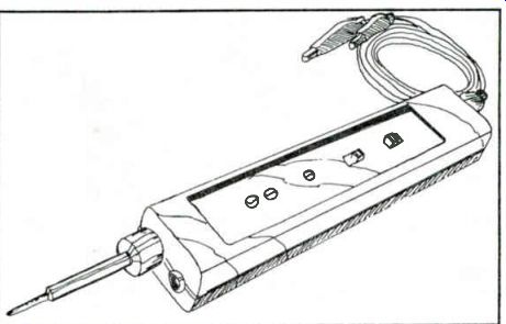
Fig. 5-15. Continental Specialties LP-3 logic probe.
Fast Pulse Catcher
The LP-3 model probe shown in Fig. 5-15 contains a unique and highly sensitive
pulse detecting system capable of catching pulses faster than 10 nanoseconds.
This insures capture of glitches and spikes for all logic families: TTL, DTL,
RTL and CMOS. The pulse detector circuit consists of a level sensitive broad
band amplifier coupled to a high-speed pulse stretching monostable multivibrator.
This circuit is capable of firing on both positive and negative transitions.
The pulse stretcher enables a 100-millisecond oscillator and LED driver circuit
that produces a visual indication of the pulse catch. The oscillator can also
be switched into a bistable mode in order to catch a pulse for memory. This
technology allows you to catch and display hidden spikes and glitches that
many scopes and logic probes will not detect. Basic rf troubleshooting techniques
are required as you try to locate these fast spikes and pulses.
The ground lead of the LP-3 must be used. Ground lines must be as short as
possible. Connect the ground lead of the probe as close to the test point as
possible. In the case of an IC, clip the ground lead directly to the IC ground
pin. The ground lead can supply the signal return and negative power line path
for the logic probe, and will help prevent ground loops.
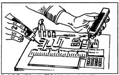
Fig. 5-16. The LP-2 and the DP-2 digital pulser probe in action.
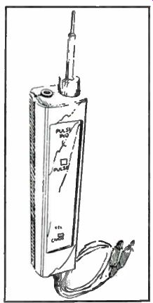
Fig. 5-17. The DP-1 digital pulser probe.
DP-1 PULSE GENERATOR PROBE
Figure 5-16 shows the E & L Instruments model MMD-1 microprocessor trainer
in the process of being checked by using Continental Specialties LP-2 logic
test probe and the DP-1 pulse generator IC probe tester. This completely automatic
pulse generator may be used for troubleshooting the more sophisticated microprocessor
and other family of digital/logic circuits. Figure 5-17 shows the DP-1.
By obtaining its power from the circuit under test, the DP-1 self-adjusts
the amplitude of its output pulse to the input requirements of the circuit
to be tested. When the pulser tip is connected to the circuit node to be tested,
the auto polarity sensing system of the probe selects the sink or power source
pulse required to activate the test point. Simply depress the push button once
to produce a clean, bounce-free pulse. When the pushbutton is held down for
more than one second, the unit produces a pulse train at a 100 pulses-per-second
rate.
The pulser has a fail-safe feature, which permits an overvoltage condition
up to 25 volts. Other built-in protection will withstand a reverse voltage
to 50 volts and allows the unit to pulse continuously into a short circuit.
The DP-1 allows the service technician all the versatility of a laboratory
quality pulse generator without the need to set pulse levels or switch to complement
the output pulses.
Auto-polarity Sensing
The pulser contains a circuit that automatically selects the sink or source
pulse needed by the circuit under test. By comparing the test point voltage
between pulses to the center of the dead zone voltage for the IC under test,
the DP-1 senses whether a "0" level is present and outputs a "1" pulse,
or if a "1" level is present it outputs a "0" pulse.
The auto-polarity sensing level is checked after each pulse to allow for changes
of state after a trigger pulse. This permits the DP-1 to trigger on RS flip-flops
supplying alternate, sink and source pulses to cross-coupled junctions to keep
the flip-flop toggled. See Fig. 5-18. This function allows you to jump from
point to point on a circuit board without regard to the logic state of the
test point.
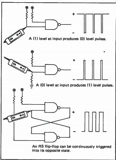
Fig. 5-18. Autosensing setup.
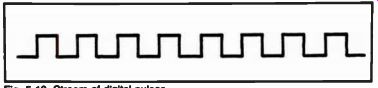
Fig. 5-19. Stream of digital pulses.
Tri-state Output
The DP-1 is a tri-state output device with a minimum of 300K ohm loading when
not being pulsed. This allows all logic ICs, including CMOS, to be unaffected
by pulse loading between pulses.
Single-Shot Mode
By depressing and releasing the push button, a single, de bounced pulse is
produced at the output. The pushbutton may be depressed as rapidly as needed
to produce a controlled stream of single pulses. Note Fig. 5-19.
The pushbutton must be released within one second in order to remain in the
single-shot mode. The LED flashes once for each single shot pulse that is produced.
Continuous Mode
When the pushbutton is depressed, a single pulse is instantly produced. If
the button is held down for more than one second, the output switches from
single-shot to continuous mode, which produces a train of pulses at 100 pulses
per second rate. The LED stays lit for continuous mode operation.
TTL Mode When the slide switch is in the TTL position, the output pulse width
is 1.5 microseconds. The pulse rise time is less than 10 nanoseconds with a
maximum 500-nanosecond storage and fall time for one TTL load. Storage and
fall time decreases as TTL loading increases. In the TTL mode, the output pulse
can sink or source 100 mA or 60 TTL loads.
CMOS Mode
When the slide switch is in the CMOS position, the output pulse
is 10 microseconds. This allows ample time for the slowest CMOS devices to
be activated. The pulse rise time is less than 100 nanoseconds, with an 8 nanosecond
storage and fall time for 100K ohm load resistance. In the CMOS mode, the output
pulse can sink or source 50 mA to a logic "1" or a logic "0" level
for any Vcc from 4 to 18 volts.
Hooking Up and Using the DP-1
The power cable of the DP-1 not only feeds power to the unit, but acts as
the return path for the output pulse. In order to decrease common moding and
ground loops, clip the power cable lead as close to the pulsing point as possible.
When power is first applied to the pulser, the LED will light and stay on for
about one second. After the LED has gone off, the pulser is ready to use.
In most cases there is no need to use the ground clip, as the unit produces
a crisp pulse under normal conditions. However, the ground lead does help the
pulser sink larger currents and can reduce pulse storage time.
If the ground lead is to be used, do not hook up the black power lead. Both
ground returns can cause common moding and ground loops which may produce false
triggering in the circuit under test.
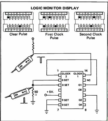
Fig. 5-20. Setup for using pulser and logic monitor.
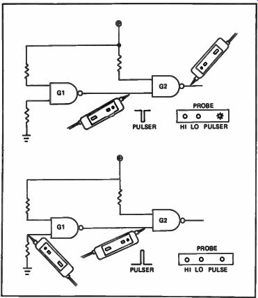
Fig. 5-21. Using the pulser to troubleshoot logic gates.
The DP-1 is an extremely effective tool to help troubleshoot digital/logic
circuits. In many cases, it is much more useful than using an oscilloscope.
Figure 5-20 shows the hookup for checking out a 7490 decade counter using
a pulser and a logic monitor. The pulser CMOS/TTL switch is set to TTL, and
the pulser tip is connected to the zero set input of the 7490. The logic monitor
is clamped onto the 7490 to display all the logic states of the counter simultaneously.
Depressing the pushbutton once puts a zero pulse into the 7490 and clears
all the outputs to zero. The pulser can now be applied to the clock input and
single step or jog the 7490 through its decade cycle.
When the counter is pulsed, all four outputs can be seen changing state, while
simultaneously monitoring the power supply input, clock inputs and clear lines.
This is one advantage of the logic monitor pulser approach over the scope,
which at best can only monitor one or two points at a time.
TROUBLESHOOTING GATES
Although logic monitors work very well on counter latches and flip-flops,
they are basically static devices and cannot display the pulsers narrow output
pulse. When troubleshooting gating and decoding systems, a logic probe is needed
for its pulse stretching abilities. The narrowest pulse of the DP-1 can be
caught and held for one-third of a second, while the HI/Lo LEDs indicate that
the node under test is high pulsing low or low pulsing high.
In Fig. 5-21A, a two-gate circuit is under test. The output of G1 is held
high, causing the output of G2 to be low. By applying the pulser to the output
of G1, the pulser overrides the output state of G1 and puts a train of zero
pulses into the gate of G2. The logic probe connected to the output of G2 has
its low LED on, but then the pulse LED starts flashing. This shows the gate
is passing the input pulses in proper polarity. In Fig. 5-21B, the probe is
moved to the output of G1, and the pulser is applied to the low gate input.
The pulser now produces a series of one pulses when the pushbutton is held
down; however, the pulse LED of the probe does not respond, indicating a defective
gate.
Logic Probe Jogging Test Technique
With the high fanout of the pulser, it has the ability of overriding the output
level set by a gate by applying the needed input pulse to the circuitry under
test. This sets the stage for system troubleshooting by using the jogging method.
A digital system can be deactivated by disconnecting the clock of the system
and replacing its pulses with those of the pulser. The complete system may
now be jogged through its cycle while different points of interest in the system
may be displayed with logic probes, logic monitors or even an oscilloscope.
Several logic monitors may be used simultaneously to display the movement
of a pulse from IC to IC, or show the response of several gates to the same
stimuli. The distinct advantages of this method become quite evident once you
have put this method into operation. You will probably find that the pulser
and logic probes are an extremely effective way to troubleshoot digital/logic
circuits and gates. With this technique, you are able to jog a logic pulse
through various gates for a FRAME-FREEZE-TIME or a slow-motion look at gate
action.
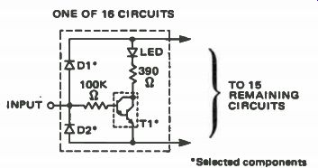
Fig. 5-22. Circuit found in logic monitor.
Logic Troubleshooting Tips
• Make sure you understand how the logic device is sup posed to operate.
• IC logic gates will very often become overheated when they are defective.
Check the temperature of these logic ICs.
• Try not to replace any components until you have zeroed in on the trouble.
• I Use the logic test probe for signal tracing and the logic pulser probe
for signal injection.
Have it well established in your mind what the circuit signal flow and
the logic levels should be.
• When troubleshooting with the logic probe, always touch the probe tip to
the IC terminal leads. Avoid the probe tip test at the IC socket.
• Use a DVM to measure the very critical voltages found in all logic circuits.
• Remove and install MOS microprocessor chips and all logic devices very
carefully. Be on the alert for any static buildup.
LOGIC MONITORS
A logic monitor test clip can be used to simultaneously display the static
and dynamic logic states of DTL, TTL or CMOS 14-pin and 16-pin digital dual-in-line
ICs. With the logic monitor, each IC lead is measured by 1 of 16 independent
binary/optical sensors.
When one of the input voltages exceeds the 2V threshold, the LED corresponding
to the activated input pin is turned on. Inputs below the threshold or uncommitted
(floating) do not activate their corresponding LEDs. A built-in power seeking
gating network locates the most positive and negative voltages applied to the
IC under test.
This network then feeds them to the internal buffered amplifiers and LED drivers.
Logic Monitor Circuit Operation
All of the 16 circuits for Continental Specialties
LM-1 logic monitor are
identical and act as buffer amplifiers, comparators and LED drivers. Selected
diodes and Darlington transistors assure the device threshold level and LED
drive capacity. Figure 5-22 shows the circuit.
When any of the remaining 14 input points is connected to a signal source
that exceeds 2V, the Darlington transistors conduct and turn on the LED in
its collector. The 100K ohm resistor in series with the base of each transistor
prevents loading of the circuit under test. The 390-ohm collector resistor
limits the LED and LM-1 current drain from the power supply system of the IC
that is being tested.
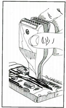
Fig. 5-23. How a logic monitor clamps on the IC.
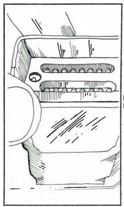
Fig. 5-24. Hewlett-Packard HP-548A logic clip probe.
Using the Clip-on Test Monitor
The logic monitor can be clamped onto any digital IC with up to 16 pins, as
shown in Fig. 5-23. Grooved pin guides ensure positive connections between
test monitor contacts and the IC leads. Static and dynamic logic levels appear
on the test LEDs for optical read out. Once clamped in place on the IC, the
logic monitor test is automatic. The Vcc or the most positive IC terminal will
be indicated by a continuously lighted LED. The least positive or uncommitted
and logic 0 IC terminals will appear as unlighted LEDs.
By reducing the system or IC input signal rate to 10 Hz or less, you will
be able to see each logic state of the IC under investigation.
Troubleshooting with the logic monitor requires a knowledge of the IC logic
pin outs. For example, consider a quad and its gate configuration. If the output
pin of one of the gates is constantly low (LED off) and gate inputs are not
simultaneously high, either the gate outputs are not simultaneously high, either
the gate output is shorted to ground internally or a short exists on the lines
fed by the gate output.
Other Logic Monitor Applications
During the design, layout and testing phases
of a new logic system, the designer has control of the variables of the system
(clock, power supplies, I/O interfaces, etc.) and can easily isolate ICs
for detailed investigation with the logic monitor. When a logic block needs
an additional gate, inverter, flip-flop, register, etc., the logic monitor
can quickly show you where unused logic gates are located within the system.
Nonfunctioning components can easily be located and replaced. Long-term testing
of individual modules can be implemented by clipping the logic monitor onto
the question able IC. This is a good check for locating intermittent troubles.
Because the entire IC can be monitored simultaneously, direct and fast visual
correlation of IC inputs and outputs simplifies and expedites signal tracing
data transfer and system fault-finding operations. System and IC reactions
to power supply changes and noise testing are other application areas that
make the logic monitor an almost indispensable troubleshooting and design instrument.
Mixed logic design DTL, TTL and CMOS, where designers take advantage of each
logic family, and also TTL or HTL outputs, are naturals for the logic monitors.
Use the logic clip when dealing with multiple PC board systems. Placing one
logic clip on the inputs or outputs of the driving/ receiving board and one
on the board under test enables you to observe the results of any modification
or stimulation on one board while making other circuit adjustments.
HEWLETT-PACKARD MODEL 548A LOGIC CLIP
The H-P Model 548A logic clip shown in Fig. 5-24 has internal self-seeking
logic circuitry so that it can be placed on a device upside-down or right side-up.
The clip locates the supply and ground pins and then starts indicating the
state of all pins. The buffered inputs of the clip draw less than 15 microamps
from signal pins, ensuring that circuit loading will not usually occur.
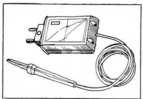
Fig. 5-25. B & K model TP-28 temperature probe.
Table 5-1. Voltmeter Conversions for the TP-28 Temperature Probe.
TEMPERATURE PROBE APPLICATIONS
The B & K model TP-28 temperature probe shown in the Fig. 5-25 is a temperature-sensitive
voltage generator that can be used with most digital or analog voltmeters as
an electronic thermometer. The voltmeter must have an input impedance of 10K
ohms or more. The meter should offer good accuracy and resolution in the 0
to 3-volt ranges. The 3½-digit B & K model 2830
digital multimeter is an ideal companion for this temperature probe. With an
autopolarity digital multimeter, the negative sign is automatically displayed
for temperature below zero degrees. Refer to Table 5-1 for the conversion of
the voltmeter voltage readings to temperature.
The TP-28 measures the temperature at the tip of the probe. It can thus be
used to measure atmospheric temperature, can be immersed to measure the temperature
of liquids, or held against a part for surface temperature measurements. The
TP-28 probe also has several non-electronic applications, such as measuring
the temperature of walls, floors and ceilings to determine where additional
insulation is needed; locating cold air leaks; and measuring the temperature
of liquids, such as water and solutions used in photo processing.
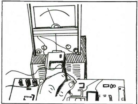
Fig. 5-26. B & K temperature probe in operation.
---------------
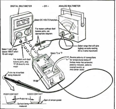
Fig. 5-27. Temperature probe connections and operations.
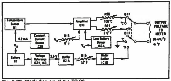
Fig. 5-28. Block diagram of the TP-28.
----------------
Using the Temperature Probe
You will find that the temperature probe has many applications in electronics.
Use it to monitor the ambient temperature at various points within a cabinet
of operating equipment and within tempera ture chambers during environmental
tests. In the design lab, it can be used to verify temperature difference between
a transistor and its heat sink to check on the amount of heat transfer. Case
temperatures can be used to evaluate biasing. The probe can be used to quickly
check out the banks of ICs found on RAM boards. A shorted RAM would be very
hot, while a cold one would indicate an inoperative one. Figure 5-26 shows
the TP-28 probe being used with a B&K model 277 FET-VOM to check temperature
of a micro processor chip.
Heat dissipation qualities of heat sinks and components can be evaluated as
conservative or marginal. The probe can be used to determine oscillator temperature/frequency
drift and measure temperature compensation parameters. The temperature probe
provides a voltage proportional to temperature which may be applied to a chart
recorder for long-term temperature measurements.
The TP-28 probe can be a very valuable test instrument for digital electronics
troubleshooting. Figure 5-27 shows the connections of the probe to the various
voltmeters and the proper operating techniques. The probe can locate hot spots
caused by shorts or partial shorts. Lack of heat indicates inoperative components.
It can also test thermal devices. An incoming inspection department could use
the probe to test temperature-related specifications of components. The circuit
block diagram of the model TP-28 temperature probe is shown in Fig. 5-28.
HANDLING MOS DEVICES
Service technicians must use caution while testing and installing MOS IC devices
that may cause damage with static electricity arcs. Some of the solid-state
devices now used in many minicomputers and color TV chassis can be damaged
with a static discharge.
You will now find the MOS IC used in a large number of consumer products.
MOS transistors are small and use little power, thus thousands of them can
be placed into an IC package that only use milliwatts of total power.
Most technicians are familiar with the single MOS transistor used for RF amplification
in TV and FM receivers. MOS ICs are now being used in complete electronic tuning
systems. They provide on-screen display of channel numbers plus time, and can
remember user-programmed channels. TV games and minicomputers use MOS circuits
extensively.
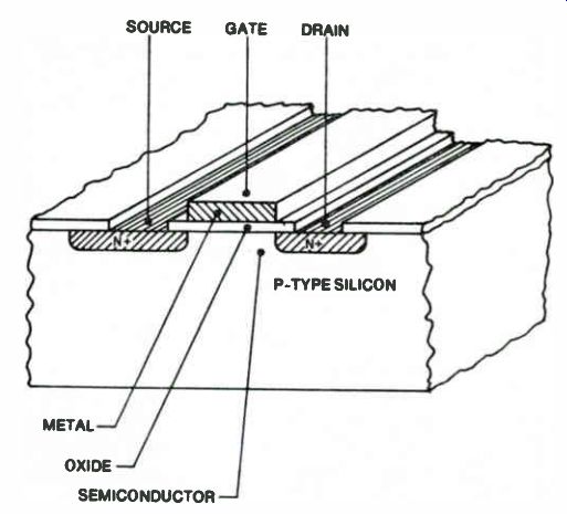
Fig. 5-29. Cross section of an MOS device.
The low-power feature of MOS circuits can cause problems when you have to
replace them. They are very sensitive to voltage spikes and static electricity.
MOS transistors are made with a thin insulating layer (oxide) sandwiched between
a gate electrode (met al) and a silicon substrate (semiconductor). Because
the oxide layer is so thin, voltages applied to the gate can influence the
properties of the underlying silicon, thus controlling current between the
source and drain. Part of the low-power feature arises because there is almost
no DC current flow required at the gate electrode.
Some engineers claim that the major cause of failures in MOS ICs is due to
breakdown of the gate oxide. Because some static electricity sparks are near
10, 000 volts, this will most certainly destroy the device when discharged
through a gate electrode of an MOS transistor. Even though static electricity
currents are small, the only discharge path is through the gate oxide, and
even small currents that pass through the oxide will cause a failure. Note
the cross-section of a MOS device in Fig. 5-29.
Inside the MOS IC, most transistors have a gate electrode driven by other
MOS devices and are protected to some degree from external static electricity.
The transistors at the input and output connections are the most susceptible
to static damage. To protect input/output devices, protection networks are
built inside the IC. These networks usually consist of diodes which bleed off
static charges to ground or power supply pins and series resistors which protect
the gate during the bleed-off process. These internal devices improve resistance
to static damage but are limited by their small size. Some static shocks are
sufficient to burn out the protection networks as well as the MOS gate oxide.
Some special techniques have been developed to protect ICs from static shock.
ICs can be shipped in metal or conductive plastic coated tubes or trays. Often
ICs will have their leads inserted into a black conductive foam or into aluminum
foil. Conductive foam and plastic envelopes or metal-lined trays are used to
transport circuit boards containing static-sensitive ICs.

Fig. 5-30. Workbench setup for servicing equipment that has MOS devices.
MOS Handling Procedures
So as not to blow out MOS devices, keep in mind that you should avoid using
any static-producing accessories. The following procedures are effective in
reducing static shock: II Just before touching any component or module, touch
the metal chassis to make sure your body is not statically charged.
• While removing circuit boards or modules from the chassis, place them on
a conductive surface, such as aluminum foil, and not on the bench.
• Touch the metal chassis just before picking up a module or component for
installation. A MOS conductive work bench is shown in Fig. 5-30.
• When removing or replacing ICs, soldering irons with grounded tips must
be used.
• Some solder suckers generate static charges when triggered on and should
not be used. Even while the IC being removed is defective, a solder sucker
can generate enough static to damage other components on the board.
Antistatic solder suckers are essential for IC removal.
• Replacement MOS ICs are packaged in conductive foam or with aluminum foil.
Do not remove the IC from its protective package until it is ready for use.
Before removing the IC, touch the conductive foam to the chassis or circuit
board in which it is to be inserted. This can be done by touching the board
with one hand and the conductive package with the other.
• Try to minimize motion when handling ICs out of the package. Clothes will
even generate static electricity when brushed against other objects.
• Do not use freon-propelled sprays on circuit boards or chassis. Freon spray
will generate static electricity. Even when an IC is in a protective package
or installed in a circuit board, freon spray can generate static electricity
which may damage internal components not directly connected to the IC pins.
--Defective components should be returned in a conductive package, not in
plastic boxes or plastic envelopes.
--Aluminum foil is an effective packaging material.
Although these tips are for MOS ICs, all IC types can be damaged by static
arcs and sparks. The more complex ICs tend to make integrated circuits even
more sensitive to static damage, although they promise a fantastic future of
improved performance and additional features in consumer products. The effectiveness
of ICs depends a lot on the ever increasing skill and knowledge of those who
troubleshoot these devices.
| Prev. | Next | Index |
Home |
This page was last updated: Friday, 2007-07-20 17:18,Tuesday, 2023-12-19 17:40
PST