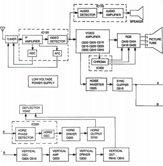

Fig. 6-1. Block diagram of a General Electric AA chassis.
| Home | Audio mag. | Stereo Review mag. | High Fidelity mag. | AE/AA mag. |
Some of the ICs found in the modern color TV chassis are almost as sophisticated as a microprocessor chip. In the first portion of this section you will see what some of the functions of these ICs are in a General Electric AA color chassis. These integrated circuits are found in the i-f and video section, synchronous demodulator, sound system, chroma chip and horizontal processor. Tips on video signal troubleshooting will then be covered.
The next section will give details on chips found in the Zenith triple-plus color chassis. This will include the master scan oscillator and vertical countdown circuits. Coverage then continues to stereo multiplex ICs and ceramic filters. The section concludes with some tips for signal tracing and troubleshooting analog IC chips.
GE COLOR TV AA CHASSIS
The functional block diagram for the GE AA chassis, shown in Fig. 6-1, illustrates the conventional solid-state design. The chassis has four ICs and we will look at some of these unique circuits in more detail.
IC 120 - I-F and Video Chip
The IC 120 chip contains not only the i-f amplifier, but the agc, afc and video detector functions as well. Two of these IC functions are not a common TV design. The agc circuit is not keyed, and the video is a synchronous demodulator.
Fig. 6-1. Block diagram of a General Electric AA chassis.
AGC Operation. The principle components in the agc system are contained in IC 120, shown in the Fig. 6-2. This is not a keyed agc system, so horizontal keying pulses are not required. Connections to the video detector and the i-f amplifier are made internally.
The only peripheral components are the rf agc network, connected to pins 3 and 4, and the agc filter components, which are connected to pin 14. The voltage on pin 14 is a good check point to measure i-f-agc. A value of 10 volts indicates maximum i-f gain, and 5 volts corresponds to minimum signal gain.
A diode keeps the voltage from going below about 4 volts. This prevents a condition called agc lock out in which RF gain is at a maximum, i-f gain is at a minimum, and there is no recognizable video output.
When the RF agc output is near 9 volts, the gain of the tuner is at maximum. As the voltage is reduced toward zero, the gain of the tuner is decreased.
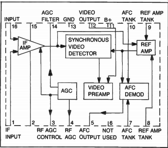
Fig. 6-2. Block diagram of an IC 120.
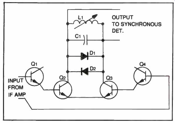
Fig. 6-3. IC 120 reference amplifier.
Reference Amplifier. The function of the reference amplifier is to filter and to limit the amplitude of the 45.75-MHz modulated signal to provide an almost pure fundamental 45.75-MHz signal as a carrier reference for the synchronous demodulator. The i-f signal is fed to the differential amplifier Q2 and Q3 through Q1 and Q4. The IC 120 reference amplifier circuit is shown in Fig. 6-3. The collector load of the differential amplifier is formed by the high-Q tuned filter L1 and C1. Because of the high Q, the filter tends to respond only to the 45.75-MHz frequency and not the sideband frequencies. Diodes D1 and D2 are connected across the filters to limit the amplitude of the reference signal. As a result, the output is a nearly constant amplitude 45.75-MHz signal.
Synchronous Demodulator. In Fig. 6-4, Q7 is a constant current source. Q1 and Q2 form a differential amplifier, and Q3 through Q6 are carrier-operated switches. The differential amplifier is fed by the i-f amplifier, and the carrier-operated switches are fed by the reference amplifier.
When the positive half cycles of the amplitude-modulated carrier appear at the base of Q1, it increases conduction. At the same time the in-phase, clipped carrier signal at the base of Q3 switches this transistor on, causing current flow through RT to increase. No current will flow through Q4; it is turned off by the reverse-phase, clipped carrier.
When the negative half cycle appears at the base of Q1, it decreases conduction, causing Q2 to increase conduction. The reverse-phase carrier turns Q4 on, causing the current through R1 to increase. No current will flow through Q3 since the in-phase carrier pulse is negative at this time.
The current flow through R1 increases for both negative and positive half cycles of the carrier, producing a waveform, as shown in Fig. 6-4D. This waveform represents the amplitude modulation which we desired to recover from the incoming signal.
170 Sound Chip
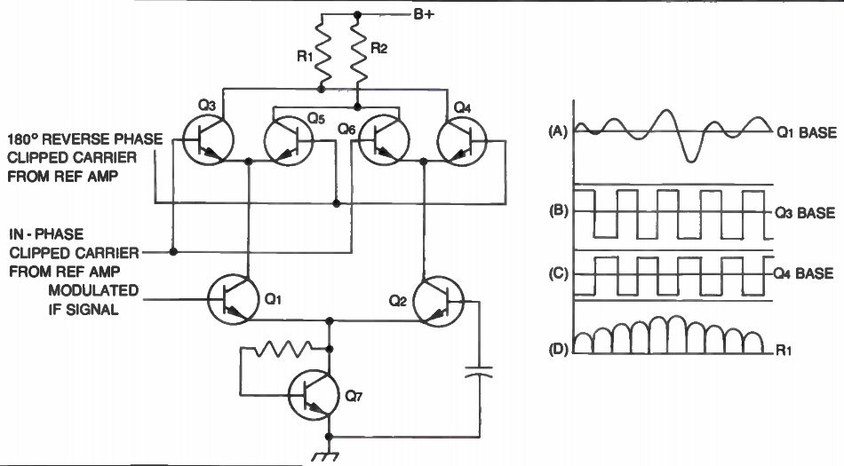
Fig. 6-4. Simplified synchronous detector circuit.
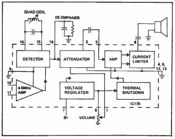
Fig. 6-5. IC 170 audio circuitry.
The IC 170 chip is a complete audio system for the GE AA chassis. It contains a 4.5-MHz amplifier, quadrature detector, electronic attenuator and audio amplifier. In addition, it contains voltage regulating, current limiting and thermal overload circuitry, as shown in the Fig. 6-5 block diagram.
The input to the 4.5-MHz amplifier is at pin 10. The amplifier is connected internally to the quadrature detector. The qual coil is connected to pins 14 and 15. The de-emphasis/tone control net work is connected to pin 16. The electronic attenuator is controlled by the voltage from the VOLUME control, which is connected to pin 1. Pin 2 is the output terminal of the attenuator. This output is capacitively coupled to pin 3, the amplifier input. The amplifier output is pin 6, and this is capacitively coupled to the speaker.
The B+ voltage for IC 170 is connected to pin 7, the input of the voltage regulator. The voltage regulator output is connected to the internal circuits and pin 8. This provides a stabilized voltage source for the VOLUME control.
Overdissipation protection is provided by the current limiting and thermal shutdown circuitry. Power dissipation of IC 170 is largely governed by the impedance of the speaker, which is 32 ohms. A lower impedance speaker would increase power dissipation.
IC 300 Chroma Chip
The chroma integrated circuit, IC 300, contains the band-pass amplifier, burst gate, 3.58-MHz oscillator, color control, color killer, APC (automatic phase control) detector and chroma demodulator functions. Refer to Fig. 6-6 for a block diagram of IC 300. The band-pass amplifier input is at pin 15. The amplifier output is connected internally to the burst gate. Horizontal keying pulses are fed to the burst gate via pin 13. The burst gate has two outputs.
One output is the chroma sideband signal, which is fed internally to the color section. The other is the gated signal that is fed from pin 17 to pin 11, the input of the APC detector. The APC ADJUSTMENT control, R324, is connected to pins 9 and 10. The 3.58-MHz crystal is connected to pins 8 and 6, and a phase-shift network connects pin 7 to pin 6. The oscillator is connected internally to the demodulator and the color killer. The color killer has no external adjustments.
The color control section is DC-controlled and has two control inputs, pins 18 and 20. Pin 18 is permanently connected for maximum gain. Pin 20 is connected to the COLOR control. The output of the COLOR control section will be found at chip pin 19.
This output signal at pin 19 goes via phase-shift networks to the demodulator inputs at pins 2, 3 and 4. The phase-shift networks provide signals of the correct phase and amplitude for the demodulator inputs. Pins 2, 3 and 4 are DC-coupled to a source voltage from pin 5 so that the demodulator DC output voltages will track each other, preventing undesirable gray scale shifts.
The TINT control circuit is connected between the outputs of the burst gate and the input of the APC detector. This is in the path of the gated burst signal. The circuit acts as a tuned RLC network, providing variable delay to the signal.
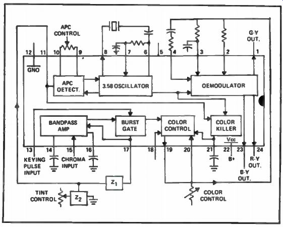
Fig. 6-6. Chroma IC block diagram.
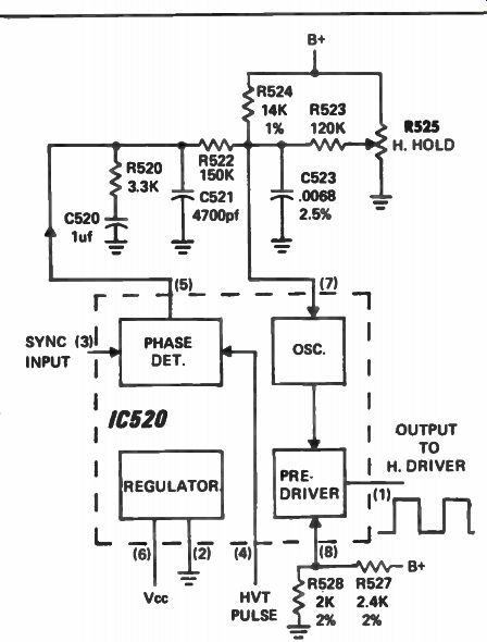
Fig. 6-7. IC 520 horizontal processor.
Because the burst signal controls the phase of the 3.58-MHz oscillator, it changes the phase angle between the 3.58-MHz reference signal and the chroma sideband signal. The variable element in the TINT control impedance network acts as a variable resistance.
As the current through it changes, its apparent resistance changes.
As a result, the impedance of that leg of the network changes, varying the delay of the color burst signal.
IC 520 Horizontal Processor
Referring to the circuit shown in Fig. 6-7, you will note that IC 520 contains the horizontal phase detector, horizontal oscillator and horizontal predriver. The sync pulse input to the phase detector is pin 3. The horizontal keying pulse enters at pin 4, and the phase detector output is at pin 5. Capacitor C521 with R520 and C520 filter the correction voltage. And R522 couples the phase detector output to the oscillator control input at pin 7.
The oscillator is an RC type with the frequency controlling components connected to pin 7. These components are C523, R523, R524 and R525. The oscillator is connected internally to the predriver.
The predriver converts the oscillator signal into a rectangular wave (pulse) which is fed out of pin 1 to the horizontal driver stage.
The duty cycle on this wave is determined by the voltage at pin 8, which is controlled very closely by the 2-percent tolerance resistors, R527 and R528. The IC has an internal regulator which holds the voltage at pin 6 to about 8 volts DC.
Video Signal Troubleshooting
The video signal path in Fig. 6-8 has five divisions that will aid you in troubleshooting. These are as follows:
-- From tuner to the output of IC 120 where the signal for the audio circuit comes off.
-- From the output of IC 120 to the collector and emitter of Q200 where the signals for the sync and color circuits come off.
-- From Q200 to C220 where DC restoration occurs. The BRIGHTNESS control is in this division.
-- From C220 to the video output of the main circuit board.
The BRIGHTNESS control is in this division.
-- From the output of the main circuit board to the CRT.
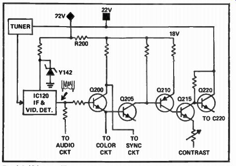
Fig. 6-8. Video amplifier stages.
These divisions will help you diagnose by symptoms. For example, if the symptom is no video but the audio is good, the trouble is not likely to be between the tuner and IC 120. Or if there is color but no video, the fault would be between Q200 and the CRT. In this case, if the BRIGHTNESS control will adjust the screen brightness, the trouble is between Q200 and Q220. Thus, you can localize the trouble by knowing where the audio, sync and color signals split off from the video signals and noting which signals are missing.
Use a scope for troubleshooting video problems. At pin 12 of IC 120, a normal video signal has negative-going sync pulses and is about 3 volt peak-to-peak. At the emitter of Q200, the sync pulses are the same polarity but they are positive-going at the collector. At C220 and at the output of the main circuit board, they are also positive-going. Use your scope to check for proper polarity and any sign of sync clipping.
Note that there are two DC-coupled sections. One of these is from pin 12 of IC 120 to the emitter of Q220. The other is from the base of Q224 to the CRT cathode. Note that this DC coupling is important because a loss of voltage at any point in the DC-coupled chain will affect the voltage in all of the stages that follow. For example, if something happens to the voltage at pin 12 of IC 120, the voltages on Q200, Q205, Q210, Q215 and Q220 will also be affected.
One other notable characteristic is that there are three voltage sources for the video signal circuits. The tuner, Q215 and Q220 are fed from a 22-volt supply developed from the 60-Hz bridge rectifier.
The color-difference amplifiers are fed from a 140-volt supply also developed from the 60-Hz bridge rectifier. IC 120 and Q200 through Q220 are fed from a 22-volt supply developed from the high-voltage transformer. Naturally, all of these voltage supplies must be working in order for the video signal stages to operate.
The last characteristic to be covered does not affect the video signal as such, but it does affect the operation of the color-difference amplifiers. The color-difference circuit is shown in Fig. 6-9. This characteristic is that the color difference amplifiers receive base bias voltage from the chroma chip, IC 300. If the base voltages are incorrect, the screen brightness or the gray scale will be affected.
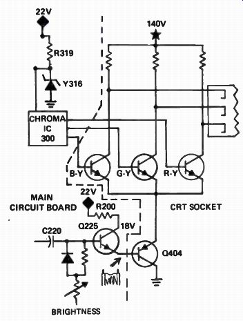
Fig. 6-9. Color-difference amplifier circuit.
ZENITH TRIPLE-PLUS COLOR CHASSIS
In this section we will be looking at the master scan oscillator, some logic circuits and vertical countdown divider circuits used in the Zenith Triple-Plus color chassis. Also, we will see some oscilloscope waveforms and troubleshooting tips for the chroma and low-level luminance ICs found in this TV chassis.
Fig. 6-10. Partial schematic of the M1 module.
Master Scan Oscillator and AGC Operation
For a discussion of these circuits, refer to Fig. 6-10, which is a partial schematic of the M1 module. The age voltage for the i-f appears at pin 13, and composite sync pulses exit at pin 3. The 503-kHz oscillator clock signal exits at pin 7 of IC 1351.
Referring to the block diagram in Fig. 6-11, let's look at some of the external components associated with the agc-sync of IC 1351.
The output of the synchronous detector is fed to pin 1 via a low-pass RC network to filter out the 4.5-MHz sound. In the IC, this signal is applied to an agc comparator. The agc comparator samples the sync tip level, compares it to a 4-volt reference level from the agc gate circuit during the gating time, and then either charges, discharges or does nothing to the primary filter capacitor C1327 at pin. The gating time is determined by the time coincidence of the keying pulse coupled to the IC at pin 16 and the sync pulses from the sync separator.
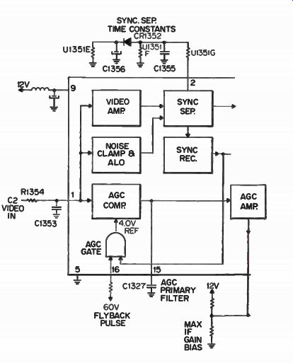
Fig. 6-11. Block diagram of the IC 1351.
The DC level of the primary filter capacitor C1327 is fed to the age amplifier. The purpose of the internal age amplifier is to limit the swing of the i-f age voltage from the maximum i-f gain point to the delay crossover point. This point is determined by the bias at pin 14 and the age delay setting of R1353 and the DELAY control at pin 13.
There is an RC external network between pin 13 and 14, which is called a feed forward circuit and allows additional gain reduction beyond the crossover point in the event of large, fast changes in signal strength. The i-f age output is filtered before it is applied to the i-f. This filter consists of resistors R1326, R1328 and capacitor C1330. Notice the zener diode in series with the AGC DELAY control. This is a 4.3-volt zener diode, and its purpose is to provide for a constant delay or crossover point independent of B+ variations. This entire circuit and others reduce the need for module adjustments or alignment when a faulty module must be replaced.
At pin 11, a forward age output is provided for the VHF tuner is provided and, at pin 12, reverse age output is provided for VHF tuner for signal strengths beyond the delay point. Video from the C2 input is fed to a video amplifier within the IC, which in turn applies it to a sync separator. The normal dual-time constant sync separator component network is located at pin 2.
At pin 4, a phase detector is within IC 1351. In addition to receiving the sync pulses, this detector also receives a sawtooth voltage generated by integrating the 60-volt positive flyback pulse by capacitors C1354 and C1352. The phase detector output is filtered at pin 10, and the noise immunity of the master scan oscillator system is determined by the value of components located at pin 10. These component values were selected with video tape viewing in mind that may have excessive skewing errors.
Within the IC, shown in Fig. 6-11, the output from the phase detector is fed to the 503.5-kHz master scan oscillator. It is refer red to as a master scan oscillator because its output frequency is not at a vertical rate, nor at the horizontal rate, but at a rate that is 32 times the 15,734-Hz horizontal frequency rate. This output is applied to the countdown IC 2126 on the M2 module which, in turn, counts down the 32 times rate (503 kHz) to the horizontal rate and an additional 262.5 times to the vertical rate. Three pins are used for this internal master scan oscillator (pins 6, 7 and 8) with the output for the vertical and horizontal countdown taken from pin 7.
The correct master scan oscillator sinewave signal that should be found at pin 7 is shown in the Fig. 6-12.
The frequency of the master scan oscillator is adjusted by shorting a test stake at pin 3, marked sync out, to ground and adjusting the core of the frequency adjustment coil L1376 for zero beat of the horizontal and vertical by looking at the TV screen to obtain the slowest roll of the picture.
Vertical Countdown System
As you refer to the block diagram in Fig. 6-13, we will discuss various points of the vertical countdown, IC 2126. This is a new Zenith chip and has a 221-103 part number. This chip accepts the 503-kHz signal from the M1 module, composite sync, and operates from 12 volts, 62 volts, and 130 volts. It provides vertical deflection, horizontal drive to the predriver, and a blanking output to the low-level luminance circuits.
As shown on the left side of Fig. 6-14, the vertical system accepts a clock signal from M1 that provides a signal to pin 9 32 times the horizontal frequency (32 H or 503 kHz). The IC divides this by 16 and then 2 (down to H) before feeding the signal into the buffer amplifier to drive the horizontal predriver located on the M3 module. In the bottom left of Fig. 6-13, the flyback pulse is compared to the incoming horizontal sync pulses in an external phase locked loop, which regulates the 503-kHz oscillator.
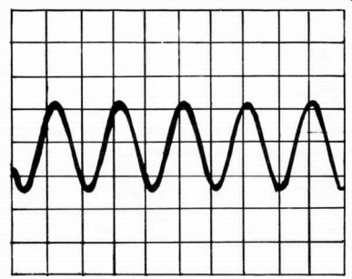
Fig. 6-12. Correct master scan sinewave signal.
The entire vertical sweep, in addition to the IC, consists of two power transistors and other peripheral circuit components. Do not look for or try to adjust the VERTICAL HOLD control because this countdown system does not require one.
Referring back to Fig. 6-14, the logic circuit provides a pulse to trigger a ramp generator. Associated with the ramp generator at pins 2 and 3 is a SIZE control and a ramp-forming capacitor.
The voltage ramp from the ramp generator is DC-coupled inside the IC to one side of a differential amplifier. The differential amplifier drives a transistor power output stage, and the output stage drives the vertical windings of the yoke. The yoke current is sensed and wave-shaped in the feedback network, and a sample of that yoke current is coupled to the feedback side of the differential amplifier at pin 5. Therefore, the differential amplifier and output stages function to make the sample of yoke current look just like the voltage ramp at its input. This technique enhances the vertical linearity. The logic section also provides a blanking pulse which is amplified by another buffer stage and coupled through pin 7 to the low-level luminance IC 2226.
The logic circuitry also has other inputs. It receives integrated vertical pulses at pin 12 to make sure that the vertical retrace interval coincides with the vertical interval of composite sync. Also, the logic circuit receives composite sync at pin 13 as it must decide if the incoming signal is standard or nonstandard. If the signal has 525 lines per frame, then the ramp generator is triggered by the countdown chain in the IC, and all of the advantages that come with a countdown result, such as good interlace and good noise immunity.
If the signal does not have 525 lines per frame, then the ramp generator is triggered by the integrated vertical pulse which still drives the yoke, but interlace and noise immunity may be affected.
Thus, the logic circuit must know if the incoming signal is standard or nonstandard. This logic circuit "looks" at the composite sync signal during the vertical interval for a period of six lines. If the signal is a standard NTSC signal, the composite sync will have proper serrations, and the logic circuit should count 12 pulse edges during the 6-line time period. If the logic period circuit does not count at least nine edges during the 6-line time period, it decides that the signal is non-NTSC or nonstandard and, therefore, does not necessarily have 525 lines.
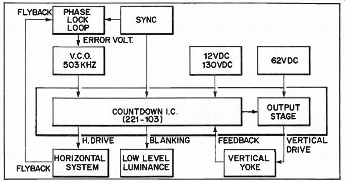
Fig. 6-13. Block diagram of vertical countdown chip.
Sync Signal Examples
Examples of nonstandard signals are those from some cable systems, some pattern generators and various types of closed circuit TV camera systems. Examples of standard signals are produced in television station transmitters and quality color-bar generators.
However, not all signals with enough serrations are standard NTSC signals with 525 lines per frame. At times, some signals might exist that can confuse the decision-making process in the logic circuit. Thus, to force the correct response, a mode override jumper is provided at pin 8 of the IC on the M2 board. If this jumper is left plugged in, the logic circuit makes it own decision about whether the signal is standard or nonstandard. If the jumper is disconnected and left open-circuited, the logic is forced into a nonstandard mode. Normally, the jumper should be left plugged in.
However in some areas, there just could be a signal where this system will not lock in the picture properly. In this rare instance, the jumper should be disconnected. The circuit should then lock onto the signal, but the advantages of countdown will be lost (interlace and noise immunity). At pin 1 of the IC, a 5-volt regulator is included. Most of the circuitry inside the IC uses 5 volts, which is generated from 12 volts. The 5 volts, filtered at pin 4 by external circuitry, is used for bias networks at pins 12 and 9.
ZENITH FM STEREO MULTIPLEX CHIP OPERATION
In this Zenith system, the FM rf signal is first processed by the rf and i-f stages before being coupled to the detector stage. The output of the detector stage is coupled to IC 301 in the phase-locked loop circuit. Depending on the type of signal received, the output of IC301 will automatically produce monaural or stereo audio information. Refer to the overall circuit and scope waveforms required for troubleshooting this FM stereo multiplex system in Fig. 6-15.
Ceramic Filters
As you can see in Fig. 6-16, there are only two tunable LC devices in the FM i-f stages. One is the first i-f transformer (1201), and the other is the quadrature coil (L205). Y201 and Y202 are the two ceramic filters used in the FM i-f stages. These ceramic filters reduce the number of tunable circuits required and also simplify alignment.
Being highly selective, ceramic filters provide approximately 75 percent of the i-f selectivity. Ceramic filters are not tunable and fall into various center frequency groups. For this reason, the signal generator must be set to the center frequency of the ceramic filters when i-f stage alignment is performed.
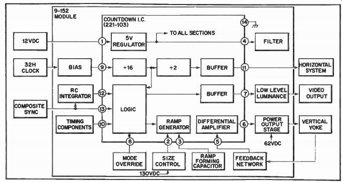
Fig. 6-14. Expanded view of an IC 2126 vertical countdown chip.
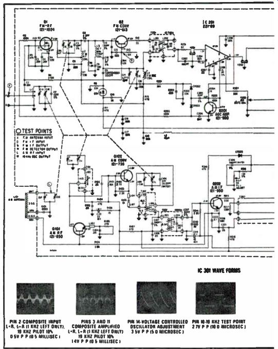
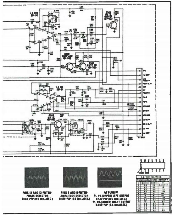
Fig. 6-15. Overall FM stereo circuit.
FM AGC Operation
Again referring to Fig. 6-16, note that agc amplifier Q201, along with the voltage doubler diodes, controls the gain of the FM rf amplifiers. A voltage divider from the FM B+ source forms the initial bias of +5.6 volts at gate 2 of the rf FET. This represents the optimum gain condition for the rf amplifier. FM signals are sampled at pin 7 of IC 201. They are coupled through C209 to the base of Q201 where the signal is amplified and coupled through C205 to the junction of CR202 and CR203. When the signal reaches sufficient amplitude, diodes CR202 and CR203 conduct, lowering the voltage of gate 2 of the rf FET from +5.6 volts, thus lowering the gain for the rf FET.
FM Multiplex Operation
The FM rf signal is first processed by the rf and i-f stages before being coupled to the detector stage. The output of the detector stage is coupled to IC 301 in the phase-locked loop circuit.
Monaural FM Mode
When a monaural rf signal is selected by the receiver, the output of IC 202 will consist of only audio information. This audio is coupled to pin 2 of IC 301. A block diagram of the phase-lock loop circuitry is provided in Fig. 6-17. The audio signal is processed by a limiter amplifier and coupled to a decoder circuit. The decoder circuit produces equal output signals at pins 4 and 5 of IC 301.
The remaining circuitry located in IC 301 is not used during monaural FM reception. The audio signal after going through the amplifier stage is coupled from pin 3 to pin 11 of IC 301 by capacitor C308. For the detector circuitry to function, a 19-kHz pilot signal must be present. This signal is present only during transmission of stereo FM.
FM Stereo Mode
It is during stereo reception that the phase-locked loop is utilized. When the FM rf tuner is tuned to a stereo station, the FM signal is processed in the rf and i-f stages as with monaural reception. The output of IC 202, the detector stage, during stereo reception contains left plus right audio as well as left minus right (23 kHz to 58 kHz) information that is amplitude-modulated with a 38-kHz suppressed carrier. In addition to these two signals, a 19-kHz pilot signal is present. The phased-locked loop circuitry must determine whether an FM monaural or FM stereo signal has been selected. The block diagram of the multiplex decoder is shown in Fig. 6-18.
Amplitude and Trigger Stage. For the amplitude detector and trigger stage to determine the presence of stereo info, a 19-kHz pilot signal and an in-phase 19-kHz signal generated by the voltage-controlled oscillator must be present simultaneously. If the pilot signal is of sufficient amplitude, a control signal will be processed by the low-pass filter and coupled to the trigger stage. The trigger stage will provide a current source for the stereo indicator lamp and simultaneously activate the stereo switch circuit. The stereo switch circuitry will allow a 38-kHz signal that is in phase with the 19-Idz pilot signal to be coupled to the demodulator.
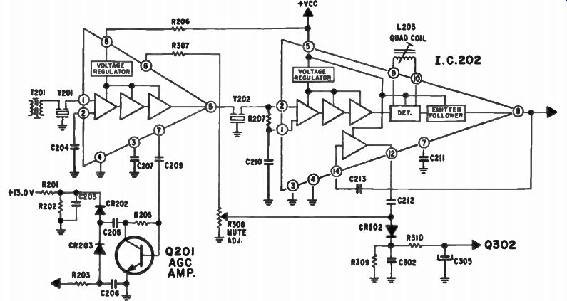
Fig. 6-16. IC 202 i-f amplifier circuits.
FM Limiter/Detector. IC 202 is the chip that receives the output from IC 201. IC 202 is the FM limiter/detector chip. A simplified illustration in Fig. 6-16 shows the functions performed within both ICs. Both IC 201 and IC 202 contain three gain/limiter stages and a voltage regulator stage. IC 202 also contains a quadrature detector, an emitter follower and a voltage amplifier.
FM Interstation Muting. Transistor Q301 also mutes the audio channel when the receiver is tuned between FM stations.
During this period of time, a noise will be present at pin 8 of IC 202.
The noise pulses are coupled through C213 to pin 14 of IC 202. The noise is amplified within IC 202 and appears at pin 12 of the IC. These noise pulses are then coupled through C212 to diode CR302.
Diode CR302 detects the amplified noise pulses and develops a positive DC voltage that is present at the base of transistor Q302.
This causes Q302 to conduct. The resultant drop in collector voltage is coupled to the base of transistor Q303. This will cause Q303 to switch off. The collector voltage at Q303 will switch towards B+. The higher positive voltage is coupled through resistors R313 and R304 to the cathode of diode CR301, turning the diode off. Thus, the signal path to transistor Q301 is opened, preventing the noise pulses from being coupled to the audio output stages.
The FM AFC Mode. The DC output at pin 8 of IC 202 is also used to provide afc action for the local oscillator in the converter stage. The DC potential at pin 8 is coupled via R212 and R11 to the cathode of varactor diode CR1. The capacitance value of CR1 is inversely proportional to the voltage applied across the diode. CR1 is connected to the local oscillator circuit in the converter stage. As the voltage across the diode increases, the capacity of the diode increases. This causes an increase in the frequency of the local oscillator. Just the opposite is true if the voltage across the diode decreases. The capacity will increase, causing a decrease in the local oscillator frequency.
If a strong station is adjacent to a weak station, the ability to tune in the weak station may be prevented by the afc action. To let you tune in a weak station, an AFC DEFEAT switch is provided on the front panel of the receiver. With the AFC switch in the off position, a fixed DC voltage is fed to the afc line from B+.
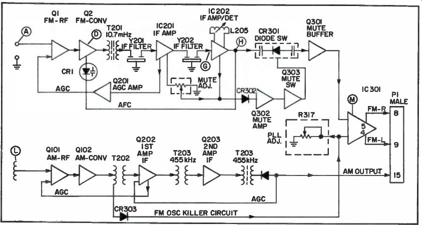
Fig. 6-17. Block diagram of phase-locked loop circuitry.
Pilot Signal Regeneration
A voltage-controlled oscillator (VCO) is used to obtain both the 19-kHz and 38-kHz signals necessary to allow stereo reception to take place. The 19-kHz pilot signal present at pin 11 of IC 301 is fed to the phase detector. Also fed to the phase detector is a second 19-kHz signal generated by the VCO. The VCO is designed to operate at 76 kHz. A divide by two stage is used to develop a 38-kHz signal that will be used to demodulate the left minus right information. A second divide by two stage is used to produce the 19-kHz signal that is coupled back to the phase detector. The phase detector will develop an error signal that is proportional to the frequency and phase differences of the two 19-kHz signals. This error signal is used to develop a DC correction voltage that is fed to the VCO. The correction voltage will cause the VCO to change frequency and phase until the resultant 19-kHz signal is identical to the phase of the pilot signals. The original 19-kHz pilot signal is identical to the phase of the pilot signal.
Also, the original 19-kHz pilot signal was in phase with the suppressed 38-kHz carrier. The regenerated 38-kHz carrier signal can now be coupled to the demodulator circuitry to be added to the left minus right information. When this has been accomplished, the left minus right audio information can be detected. The two audio signals, left plus right and left minus right, are then demodulated to reproduce left and right channel information.
Analog IC Chip Testing
An IC checker for general consumer product troubleshooting is not yet practical, and the cost would be too great. The next best technique for the technician to troubleshoot these chips is to consider the IC as a black box. For this testing concept, you must know what signal input to expect and what the output should be. Thus, by using an oscilloscope for measuring the input and output signals, you can determine whether or not the IC is good. This black box chip testing method is illustrated in Fig. 6-19 as it could be applied to an FM stereo multiplex decoder IC package. For these checks you need a FM stereo generator and a high-gain, wide-band oscilloscope. The first step would be to make sure all DC voltages to the IC are correct. Then check for proper composite FM stereo signal at pin 3 of the IC 301 with the scope. All other active pins on the chip can now be checked with the scope for expected waveforms that are shown at the bottom of Fig. 6-19. This same technique can be used to check the in and out of ICs used in i-f amplifiers, audio amplifiers, FM detectors, chroma amplifiers and demodulators. The presence of a signal may also be checked with a VTVM by using a diode detector probe for rf signals.
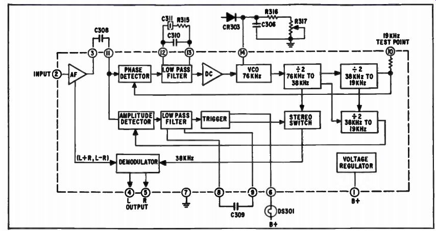
Fig. 6-18. Block diagram of a multiplex decoder.
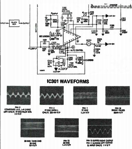
Fig. 6-19. Stereo multiplex decoder IC schematic and black box chip testing.
With this signal tracing concept for testing ICs, you must know what output to expect for a given amount of signal input. When checking an i-f or audio IC amplifier you not only need to know the gain and any control bias data of the chip, but also the frequency range of the input signal for the expected gain. In many cases, this information can be found in the service information data usually supplied by the manufacturer.
Tuned Circuit IC Testing
In some cases, you may want to check the rf signal path through an IC with tuned signal input and output transformer stages. Signal injection may be required so as not to disturb the tuned circuits. Inductive coupling can be used to inject the test signal and to measure the output. A test probe can be fashioned by winding a coil on one end of a small ferrite rod. Or you can use a discarded radio or video i-f coil. For circuits that use unshielded coils, slip an air-core coil over the tuned coil under test, which causes less detuning than a ferrite-core coil. The scope probe is connected to the output of the circuit with the same type of coil, thus achieving complete instrument inductive coupling.
The generator should be terminated with the correct resistance across the input coil. Some generators may have the proper termination built into the cable leads. Shunt the pick-up coil with a 1500-ohm termination resistor and connect the scopes rf detector probe across it. Figure 6-20 shows the complete test setup.
CAUTION NOTE: Always use the minimum amount of generator signal that will provide an output indication on the scope.
For best results use minimum generator output and more vertical scope gain while maintaining very loose coupling. Check alignment after any fault has been found and corrected. For a resonance check of a single unshielded coil, it's best to use a grid-dip or tunnel-dipper meter.
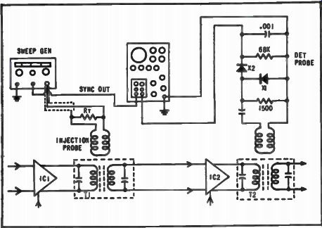
Fig. 6-20. Signal generator and scope test setup for inductive IC checks.
To recap, IC troubleshooting, remember there is no practical IC checker that you can now use. Thus, you should verify that the supply voltages (Vcc) are correct and that the DC voltages at the pins of the IC are within tolerance. If correct input signal is then present but other symptoms and output scope waveforms indicate a faulty IC, then substitute a known good chip and recheck the operation of the set.