AMAZON multi-meters discounts AMAZON oscilloscope discounts
Resistors, capacitors and inductances are known as passive components.
Devices which produce changes in circuit conditions by reacting to applied signals are known as active components. The majority of active components used in modern electronic circuits are semiconductors, or more correctly put, devices based on semiconductor materials.
Put very simply, a semiconductor material is one which can be given a predominance of mobile negative charges or electrons, or positive charges or "holes." Current can flow through the material from the movement of both electrons and holes. This is quite different from the behavior of a normal conductor, where current flow is the result of electrons through the material (see Section 1).
Semiconductor properties can be given to a strictly limited number of materials by "doping" with minute traces of impurities. The two main semiconductor materials are germanium and silicon (both non-metals or "semi metals"). Doping can produce a material with either a predominance of Positive charges (holes) resulting in a P-type material; or with a pre dominance of Negative charges (electrons), known as an N -type material.
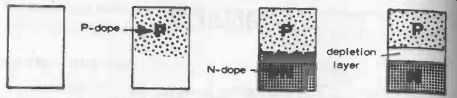
Fig. 9-1. Four stages in the construction of a semiconductor diode, shown
in simple diagrammatic form.
This does not become particularly significant until a single crystal (or germanium or silicon) is treated with both a P-type dope and an N -type dope. In this case, two separate regions are formed-a P-region and an N-region. Since these regions have opposite charges there will be a tendency for electrons to migrate from the N-zone to the P-zone, and holes to migrate from the P -zone into the N -zone. The effect will be a cancellation of charges in the region of the junction of the P- and N -zones, forming what is called a depletion layer, Fig. 9-1. This layer, which contains no free electrons or holes, will then act as a barrier between the P -zone and the N -zone, preventing any further migration of either electrons or holes. In effect, the
barrier or depletion layer sets up a potential difference between the regions and the device remains in a stable state until an external voltage applied to it.
Figure 9-2 shows what happens when an external voltage is applied to the device. In the first diagram, the + voltage is connected to the P-zone.
Provided this voltage is sufficiently high to overcome the potential difference setup in the construction of the device (which may be only a few tenths of a volt( it will repel holes in the P-zone towards the N -zone, and attract electrons in the N -zone into the P -zone. Effectively, the barrier or depletion layer will disappear and current will flow through the device.
Voltage applied this way is known as forward bias.
If the external voltage is applied the other way, as in the second diagram, the opposite effect is created, i.e., the thickness of the depletion layer will increase, thus building up a higher potential in the device, opposing the external voltage. The back voltage developed will be equal to that of the applied voltage, so no current will flow through the device.
Voltage applied this way is known as negative bias.
The device just described is a semiconductor diode. It has the basic characteristic of acting as a conductor when connected to an external voltage one way (forward bias), and as an insulator when connected the other way (reverse bias).
Diode characteristics will be described in some detail later on, but having established the electronic picture of a diode, the same principles can be applied to explain the working of a transistor.
TRANSISTORS
Basically, a transistor is two diodes placed back-to-back with a common middle layer, the middle layer in this case being much thinner than the other two. Two configurations are obviously possible, PNP or NPN (Fig. 9-3). These descriptions are used to describe the two basic types of transistors. Because a transistor contains elements with two different polarities (i.e., P- and N -zones), it is referred to as a bipolar device, or bipolar transistor.
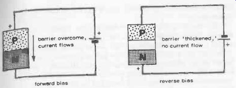
Fig. 9-2.
The two modes in which a diode can be worked.
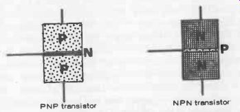
Fig. 9-3. Construction of a PNP and a NPN transistor, shown in simple diagrammatic
form.
A transistor has three elements, and to operate in a working circuit it is connected with two external voltages or polarities. One external voltage is working effectively as a diode. A transistor will, in fact, work as a diode by using just this connection and forgetting about the top half. An example is the substitution of a transistor for a diode as the detector in a simple radio.
It will work just as well as a diode because it is working as a diode in this case.
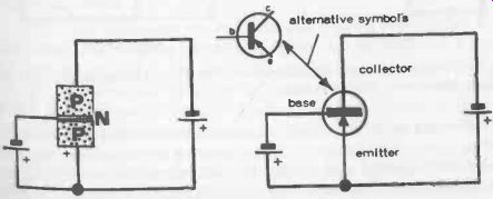
Fig. 9-4. Bias and supply connections to a PNP transistor shown diagrammatically
(left) and in symbol form (right).
The diode circuit can be given forward or reverse-bias. Connected with forward bias, as in the first diagram of Fig. 9-4, drawn for the PNP transistor, current will flow from P to the bottom N. If a second voltage is applied to the top and bottom sections of the transistor, with the same polarity applied to the bottom, the electrons already flowing through the bottom N section will promote a flow of current through the transistor bottom-to-top.
By controlling the degree of doping in the different layers of the transistor during manufacture, this ability to conduct current through the second circuit through the resistor can be very marked. Effectively, when the bottom half is forward biased, the bottom section acts as a generous source of free electrons (and because it emits electrons it is called the emitter). These are collected readily by the top half, which is consequently called the collector, but the actual amount of current which flows through this particular circuit is controlled by the bias applied at the center layer, which is called the base.
Effectively, therefore, there are two separate working circuits when a transistor is working with correctly connected polarities, Fig. 9-5. One the loop formed by the bias voltage supply encompassing the emitter and base. This is called the base circuit or input circuit. The second is the formed by the collector voltage supply and all three elements of the transistor. This is called the collector circuit or output circuit. (Note: this description applies only when the emitter connection is common to both circuits-known as common emitter configuration. This is the most widely used way of connecting transistors, but there are, of course, two other alternative configurations--common base and common collector. But the same principles apply in the working of the transistor in each case).
The particular advantage offered by this circuit is that a relatively small base current can control and instigate a very much larger collector current (or, more correctly, a small input power is capable of producing a much larger output power). In other words, the transistor works as an amplifier.
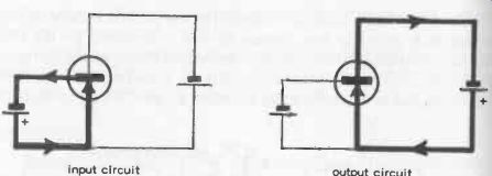
Fig. 9-5. The two separate circuits involved in working a transistor. Direction
of current flow is for a PNP transistor.
With this mode of working, the base -emitter circuit is the input side, and the emitter through base to collector circuit is the output side. Although these have a common path through base and emitter, the two circuits are effectively separated by the fact that, as far as polarity of the base circuit is concerned, the base and upper half of the transistor are connected as a reverse biased diode. Hence there is no current flow from the basic circuit into the collector circuit.
For the circuit to work, of course, polarities of both the base and collector circuits have to be correct (forward bias applied to the base circuit, and the collector supply connected so that the polarity of the common element (the emitter) is the same from both voltage sources).
This also means that the polarity of the voltages must be correct for the type of transistor.
In the case of a PNP transistor, as described, the emitter voltage must be positive. It follows that both the base and collector are negatively connected with respect to the emitter.
The symbol for PNP transistor has an arrow on the emitter indicating the direction of current flow, i.e., always towards the base. (P for positive, with a PNP transistor).
In the case of an NPN transistor, exactly the same working principles apply but the polarities of both supplies are reversed, Fig. 9-6. That is to say, the emitter is always made negative relative to base and collector (N for negative in the case of an NPN transistor). This is also inferred by the reverse direction of the arrow on the emitter in the symbol for an NPN transistor, i.e., current flow away from the base.
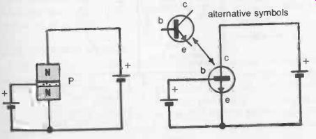
Fig. 9-6. Bias and supply connections to an NPN transistor, shown diagrammatically
(left) and in symbolic form (right).
PRACTICAL DIODES
The typical appearance of a semiconductor diode is shown in Fig. 9-7.
The cathode end is usually marked by a red dot or color band, or a + sign, and also usually with a type number consisting of one or more letters followed by figures. This identifies the diode by manufacturer and specific model. Specific type numbers are usually quoted for specific circuit de signs, but many circuits are fairly noncritical as regards the type of diode used.
Diodes may also be described in more general terms by the crystal material (germanium or silicon), and by construction. Here, choice can be more important. Germanium diodes start conducting at lower voltages than silicon diodes (about 0.2 to 0.3 volts, as compared with 0.6 volts), but t to have higher leakage currents when reverse biased, this leakage current increasing fairly substantial with increasing temperature. Thus, the germanium diode is inherently less efficient as a rectifier than a silicon di especially if reverse bias current is high enough to produce appreciable heating effect. On the other hand, a germanium diode is preferred to silicon diode where very low operating voltages are involved starts to conduct at a lower forward voltage.
The construction of a diode governs both its current-carry capabilities when conducting, and its capacitance effect. The larger junction area of a diode, the higher the current it can pass without overheating--this characteristic being desirable in high-power rectifier for example. On the other hand, increasing the junction area increases readiness with which a diode will pass ac due to inherent capacitance effects. To reduce this effect to a minimum, a diode can be made from single doped crystal (usually N-type), on which the point of a piece of spring wire rests. The end of this wire is given opposite doping (P-type). This diodes reduces the junction area to a minimum, such as a diode being known as a point -contact type. It is a favored type for use in circuits carrying high frequency ac signals, and for this reason is sometimes called a signal diode.
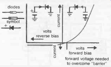
Fig. 9-7. Working characteristics of a typical semiconductor diode. GEM symbol
1.7 volts reverse-bias a volts -0 forward bias forward voltage needed to overcome "barrier".
The typical characteristics of a diode are also shown in simple graphical form in Fig. 9-7. Bias is represented by the voltage applied to the positive side, specifically referred to as anode voltage. Current flowing through the diode is referred to as anode current.
With forward bias (positive voltage applied to the anode end of the diode), there will be at first no anode current until the inherent barrier voltage has been overcome (0.3 volts for a germanium diode; 0.6 volts for silicon diode-regardless of the construction of either type). Any further increase in anode voltage will then produce a steep rise of anode current. In practice, it is necessary to limit this current with a resistor or equivalent resistive load in the circuit to prevent the diode being overheated and the junction destroyed.
With reverse bias (negative voltage applied to the anode end of the diode), the only current flowing will be a very small leakage current of the order of microamps only, and normally quite negligible. This leakage current does not increase appreciably with rise in (negative) anode voltage, once it has reached its saturation value.
It will be appreciated that a diode will work in both a dc and an ac circuit. In a dc circuit, it will conduct current if connected with forward bias.
If connected the opposite way, it will act as a stop for current flow. An example of this type of use is where a diode is included in a dc circuit-say the output side of a dc power supply-to eliminate any possibility of reverse polarity voltage surges occurring which could damage transistors in the same circuit (see Fig. 26-1).
In an ac circuit a diode will "chop" the applied ac, passing half cycles which are positive with respect to the + end of the diode, and stopping those half cycles which are negative with respect to + end of the diode. This is rectifier action, widely used in transforming an ac supply into a dc output.
The same action is required of a detector in a radio circuit. Here the current applied to the diode is a mixture of dc and ac. The diode detector transforms this mixed input signal into a varying dc output, the variations following the form of the ac content of the signal.
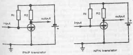
Fig. 9-8. Simple current bias circuits for transistor working.
BASIC TRANSISTOR CIRCUITS
The transistor in common-emitter configuration works as an amplifier, as previously explained. It needs two separate supply voltages--one for bias and the other for the collector--but these do not necessarily have to come from separate batteries. They can be provided by a single supply (battery) taken to the common connection (the emitter) and the collector, and tapping the collector side to apply the necessary forward bias voltage to the base, dropped through a bias resistor.
A basic amplifier circuit then looks like Fig. 9-8.
To make the circuit do useful work, the collector current has to be fed through an output load, such as a load resistor. These two diagrams also show clearly input and output as separate entities, and can clarify the point about amplification. The power derived in the output is far greater than that put into the input.
This very simple method of supplying both collector and bias voltages from a single source is known as current biasing. It needs only one resistor, and it works. The resistor value is chosen to give a base -emitter voltage of the order of 0.1 to 0.2 volts for germanium transistors ; and about 0.6 to 0.7 for silicon transistors. It is not as stable as it should be for many circuits, however, particularly if a germanium transistor is used. Thus voltage bias is often preferred--Fig. 9-9.
With voltage bias, two resistors (R1 and R2) are used to work as a divider. A resistor (R3) is also added in the emitter line to provide emitter feedback automatically, to control the bias voltage under varying working conditions. This latter resistor is also usually paralleled with a capacitor to provide further stabilization (but this may be omitted with silicon transistors).
Determination of suitable component values is now more complicated since three resistors are involved. The actual base voltage can be calculated from the following formula:
base voltage - R2x supply voltage (R1 + R2)
The emitter voltage will be equal to this less the voltage between base and emitter (across the transistor). In most cases, a voltage drop of 1 volt in the case of germanium transistors and 3 volts with silicon transistors is the design aim. The emitter resistor (R3) also needs to be quite large so that there will be minimal changes in emitter current with any variation in supply voltage. This can cause a little re -thinking about suitable values for R1 and R2, for the voltage developed across R3 must be very much greater than the voltage developed by the base current across the source resistance formed by the parallel combination of R1 and R2.
TRANSISTOR CONSTRUCTION
The original transistors were made from germanium crystals with point-contact construction. Later types, with considerably improved performance, are of alloy junction or alloy-diffusion construction. Silicon transistors are usually made by the planar process (silicon planar process).
Their characteristics can be further improved by adopting a modified planar process described as epitaxial, basically involving a preliminary process of forming an oriented layer (epitaxial layer) of lightly doped silicon over the silicon substrate. The transistor elements are subsequently formed within the layer rather than within the silicon substrate itself (as in the normal planar process). Epitaxial silicon planar transistors have superior characteristics for high frequency applications, notable in rf and i-f circuits for superhet radios.
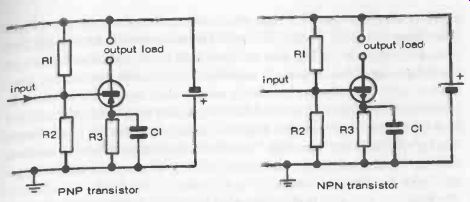
Fig. 9-9. Voltage bias circuits for transistor working.
Germanium and Silicon Transistors
Just like diodes, transistors are made from either germanium or silicon crystals. Germanium transistors have low voltage losses but their characteristics are more liable to vary with temperature, so that the spread of characteristics under which they work in a circuit can be quite wide. They are also limited to a maximum working temperature of about 100° C.
Silicon transistors are generally more stable and can operate at temperatures up to 150° C or more. They have lower leakage losses and higher voltage ratings, and are generally far better suited for use in high frequency circuits.
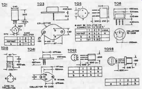
Fig. 9-10. Some common transistor outlines (diagrams by Electro-value, all
dimensions in inches).
The Shape of Transistors
Transistors come in all sorts of shapes and sizes. However, the only problem where a specified type of transistor is to be used is correctly identifying the three leads. The position of these can be identified reference to Fig. 9-10. The most common lead configuration is in line, with a circular case, when the leads follow in logical order-collector, base emitter, with the collector lead being more widely spaced from the mid, (base) lead than the emitter lead, looking at the bottom of the transistor, from where the leads emerge. This does not apply when the case is partially circular with a flat on one side. Here the three leads are equi-spaced and with the flat side to the left (and looking at the bottom), the lead arrangement may be bce, cbe, or ebc.
Power transistors are more readily identified by their elongated bottom with two mounting holes. In this case there will only be two leads emitter and base-and these will normally be marked. The collector: connected internally to the can, and so connection to the collector is via o of the mounting bolts or bottom of the can.
FIELD-EFFECT TRANSISTORS
The Field-Effect Transistor(or FET) is really a different type of semi conductor device to a bipolar transistor, with characteristics more like a vacuum tube than a bipolar transistor. Its correct definition is a unipolar transistor. The way in which it works can be understood by presenting it in electronic picture form as in Fig. 9-11, where it can be seen that it consists of a channel of either P-type or N-type semiconductor material with a collar or gate of opposite type material at the center. This forms a semiconductor junction at this point. One end of the channel is called the source, and the other end the drain.
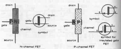
Fig. 9-11. Construction of field-effect transistors shown in simple diagrammatic
form, together with appropriate symbols for FETs.
An FET is connected in a similar manner to a bipolar transistor, with a bias voltage applied between gate and source, and a supply voltage applied across the center of the channel (i.e., between source and drain). The source is thus the common connection between the two circuits.
Compared with a bipolar transistor, however, the bias voltage is reversed.
That is, the N-gate material of a P-channel FET is biased with positive and the P -gate material of an N-channel FET is biased with neg. voltage, Fig. 9-12. This puts the two voltages in opposition at the source, which is responsible for the characteristically high input voltage, Fig. 9-12.
This puts the two system voltages in opposite resistance of FETs.
The effect of this reverse bias is to form an enlarged depletion layer in the middle of the channel, producing a "pinching" effect on the flow of electrons through the channel and consequently on the current flow in the source-to-drain circuit. If enough bias voltage is applied, the depletion layer fills the whole gate ("shuts the gate"), causing pinch off, when the source-to-drain current falls to zero (in practice nearly to zero, for there will still be some leakage). With no bias applied to the gate, the gate is wide open and so maximum current flows.
In effect, then, the amount of reverse bias applied to the gate governs how much of the gate is effectively open for current flow. A relatively small change in gate voltage can produce a large change in source-to -drain current, and so the device works as an amplifier. In this respect, a P-channel FET works very much like a PNP transistor, and an N -channel FET as an NPN transistor. Its main advantage is that it can be made just as compact in size, but can carry much more power.
In this respect-and the fact that it has a high input resistance, whereas a bipolar transistor has a low input resistance--it is more like a tube in characteristics than a bipolar transistor. It also has other advantages over a bipolar transistor, notably a much lower inherent "Noise," making it a more favorable choice for an amplifier in a high-quality radio current.
The type of field-effect transistor described is correctly called a junction field-effect transistor, or JFET. There are other types produced by modifying the construction.
The insulated -gate field-effect transistor, or IGFET is self-explanatory.
The IGFET has even higher input resistance (because the gate is insulated from the channel), and is also more flexible in application since either "reverse" or "forward" polarity can be applied to the N -channel FET P-channel FET gate for bias. FETs, of either type, can also be made with two gates.
In this case the first gate becomes the signal gate (to which the input signal is applied) and the second gate becomes the control gate, with similar working to a pentode tube (see Section 12).
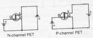
Fig. 9-12. Basic bias requirements for field-effect transistors.
FETs are also classified by the mode in which they work. A JFET works in the depletion mode, i.e., control of the extent of the depleting layer, and thus the "gate opening" being by the application of a bias voltage to the gate. An IGFET can work in this mode, or with opposite bias polarity in which case the effect is to produce an increasing "gate opening," with enhanced (increased) source-to-rain current. This is called the enhancement mode.
An FET designed specifically to work in the enhancement mode has no channel to start with, only a gate. Application of a gate voltage causes a channel to be formed.
The basic circuit of an FET amplifier is very simple, Fig. 9-13 (with polarity drawn for a P -channel FET). Instead of applying a definite negative bias to the gate, a high value resistor (R1) is used to maintain the gate at substantially zero voltage. The value of resistor R2 is then selected to adjust the potential of the source to the required amount positive to the gate.
The effect is then the same as if negative bias were applied direct to the gate. This arrangement will also be self -compensating with variations in source-to-drain current. The third resistor, R3, is a load resistor for the FET to set the design operating current. Capacitor C1 acts as a conductive path to remove signal currents from the source.
Both junction -type (WET) and insulated gate (IGFET) field-effect transistors are widely used, the latter having the wider application, particularly in integrated circuits. The metal -oxide semiconductor FET, generally referred to as a MOSFET, can be designed to work in either mode, i.e., as a depletion MOSFET, or enhancement MOSFET. The former usually an N -channel device and the latter a P -channel device. P-channel MOSFETS working in the enhancement mode are by far the more popular, mainly because they are easy to produce. In fact, an N -channel MOSFET can be made smaller for the same duty, and has faster switching capabilities, and so really is to be preferred for LSI MOS systems (see also Section 13).
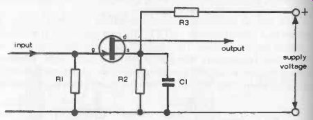
Fig. 9-13. Basic FET amplifier circuit. Performance is generally superior
to that of a bipolar transistor amplifier.