FIG.1 Basic CMOS inverter circuit
| Home | Audio mag. | Stereo Review mag. | High Fidelity mag. | AE/AA mag. |
SECTION 1 - INTRODUCTION TO CMOS
Although CMOS I.C.s are a range of digital devices, they are suitable for a range of applications which is far more diverse than one might expect. In fact, there can be little doubt that these I.C.s are the most useful range of digital devices for the average amateur user, and are perhaps even the most useful range of I.C.s of any type.
When CMOS devices were first introduced in the early 1970s they were much more expensive than their alternatives in other logic families. This is not the case these days, and they are now about the cheapest I.C.s available. The more simple of the devices in the CMOS range cost less than many ordinary transistors, and on a cost basis these I.C.s are just about unbeatable.
Earlier families of digital devices suffer from three main disadvantages which limit their usefulness to the amateur. They require relatively high supply currents (about 20 mA for a simple quad gate I.C.), supply voltages are rather critical (5 V +/- 10% for TTL devices for instance), and input impedances are usually rather low, often being only in the region of a few hundred ohms.
CMOS devices do not have any of these disadvantages. They require only very modest supply currents, and even some quite complex devices, such as the 4046 low frequency phase locked loop will operate at supply currents of less than 1 mA. Simple gates, when they are in a static condition, use virtually no power at all.
The supply voltage range over which a CMOS device will operate depends upon the suffix given after the type number. The devices usually supplied to amateur users, and specified for the projects in this book, have an 'AE' suffix. The 'A' of the suffix denotes that the unit has an operating voltage range of 3 to 15 V, and the 'E' indicates that it is contained in a standard DIL plastic encapsulation.
Input impedances of CMOS I.C.s arc extremely high indeed, being something in the order of 1,000,000 Megohms. For all practical purposes they can be regarded as having an infinite input impedance, and are voltage rather than current operated devices.
Basic Gates
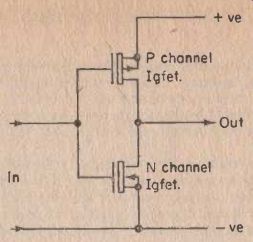
The most simple of CMOS devices is the inverter, which uses only two active devices. The circuit of an inverter is shown in Figure 1.
This uses a single P Channel Igfet (insulated gate field effect transistor) and one N Channel Igfet.
This is, of course, a switching device and the input is therefore only maintained in one of two states. It is either high, which means that it is at or near the positive supply potential, or it is low, which means that it is at or near the negative supply potential.
FIG.1 Basic CMOS inverter circuit
These states are often referred to as logic 1 and logic 0 respectively.
The output of the circuit can also have only two stable states, and again these are the high and the low states. The purpose of the inverter, as its name suggests, is to have an output state which is the opposite of the input one.
Operation of this circuit is quite simple to understand. An Igfet has a very high drain to source resistance when its gate is at around the same potential as its source. If a forward bias of a couple of volts or more is applied to its gate then the drain to source resistance falls to a value of only a few hundred ohms.
Thus, when the input of the inverter is low, Tr1 is turned hard on and Tr2 is hard off, and the output of the device is in the high state. When the input is high, Tr1 is off and Tr1 is on, and the output is low. The transistors are acting as simple S.P.S.T. switches, and Figure 2(a) shows the effective circuit of the unit in the high output state, and Figure 2(b) shows the effective low output circuit.
One could gain the impression from this that the circuit never consumes any current, but this is not the case. The transistors do not form perfect switches, and they have a resistance of a few hundred ohms when on, and a few thousand Megohms when off. Thus a minute, but for most purposes an insignificant current does flow through a static inverter.
A very brief pulse of current is consumed by the device as it changes state, as in effect, one switch closes before the other opens as the
----------
FIG. 1 Basic CMOS inverter circuit
high, which means that it is at or near the positive supply potential, or it is low, which means that it is at or near the negative supply potential.
These states are often referred to as logic 1 and logic 0 respectively.
The output of the circuit can also have only two stable states, and again these are the high and the low states. The purpose of the inverter, as its name suggests, is to have an output state which is the opposite of the input one.
Operation of this circuit is quite simple to understand. An Igfet has a very high drain to source resistance when its gate is at around the same potential as its source. If a forward bias of a couple of volts or more is ' applied to its gate then the drain to source resistance falls to a value of only a few hundred ohms.
Thus, when the input of the inverter is low, Tr1 is turned hard on and Tr2 is hard off, and the output of the device is in the high state. When the input is high, Tr1 is off and T r1 is on, and the output is low. The transistors are acting as simple S.P.S.T. switches, and Figure 2(a) shows the effective circuit of the unit in the high output state, and Figure 2(b) shows the effective low output circuit.
One could gain the impression from this that the circuit never consumes any current, but this is not the case. The transistors do not form perfect switches, and they have a resistance of a few hundred ohms when on, and a few thousand Megohms when off. Thus a minute, but for most purposes an insignificant current does flow through a static inverter.
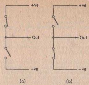
FIG.2 (a) The effective high output circuit, and (b), the effective low output
circuit
A very brief pulse of current is consumed by the device as it changes state, as in effect, one switch closes before the other opens as the circuit goes from one output state to the other. Therefore, the more frequently the device changes state, the higher its current consumption.
When used at fairly low frequencies CMOS I.C.s have very low current consumptions, but when used at high frequencies the current consumption can rise to many mA per device. Because of this it is usual to confine the use of CMOS I.C.s to medium and low speed applications.
Many of the projects described in this book are based on inverters, but these are not of the type just described. Instead, it is more convenient in use to use NOR and NAND gates with the inputs connected in parallel. For most circuits either a 4001 quad two input NOR gate or a 4011 quad two input NAND gate is specified. Four inverters can be made from each device, and they have the same characteristics as the basic inverter just described.
Manufacturers
CMOS I.C.s are manufactured by more than one company, and each company uses a different prefix to the type number. Most CMOS I.C.s offered to the amateur seem to originate from R.C.A. and have their CD prefix (CD4011AE for example). Some firms offer Motorola devices which have a 1 prefix (such as 14011), and others just give the basic type number.
Any of these I.C.s will work perfectly well in the circuits described here.
CMOS Protection
As many readers will be aware, Igfets are easily damaged by high voltage static charges. Such charges exist in most households these days due to the widespread use of plastics which tend to generate static charges. Even someone wearing a nylon shirt is said to be a potential source of destruction as far as an Igfet is concerned.
One might think that CMOS devices were very delicate, and virtually impossible to use. This is not in fact the case, as all recent CMOS I.C.s are equipped with internal protective diodes which limit voltages at the inputs to a safe level.
Even so, it is still advisable to obey a few simple rules when handling and using CMOS I.C.s. These devices axe usually supplied with their leadouts embedded in a piece of conductive foam. It is a good idea to leave the device in this foam until it is actually going to be used.
Do not plug or unplug a CMOS I.C. from an I.C. holder while the supply is connected. Make quite sure that the supply is connected with the correct polarity. When using I.C. holders it is an easy matter to accidentally plug an I.C. into a socket the wrong way round. This results in the supply being connected with incorrect polarity, and almost certainly causes the destruction of the device when the power is switched on.
In many of the circuits to be described here, some of the gates of an I.C. are not used. It is not a good idea to simply ignore the unused gates. There is little risk of the gates being damaged by static charges and other sources of electrical signals, but these will operate the inputs of the gates.
As mentioned earlier, a static gate uses no significant current, but it is switching continually from one state to the other, it will use supply current. Therefore, the inputs of unused gates should be connected to one or other of the supply lines (whichever happens to be the most convenient), as otherwise stray pick up will operate the gates causing a waste of power.
Final Points
CMOS devices have a wide operating temperature range, the actual range being -40 to +85 degrees centigrade for the plastic DIL versions (-55 to +125 degrees centigrade for the ceramic and flatpack versions).
They are therefore perfectly suitable for use in automotive and similar outdoor applications.
If the output of a CMOS device should happen to be accidentally short circuited to one of the supply lines, a current of many mA will flow.
The amount of current that flows will depend upon the power supply voltage used, but the resistance of the output transistor which is turned 4 CMOS Protection As many readers will be aware, Igfets are easily damaged by high voltage static charges. Such charges exist in most households these days due to the widespread use of plastics which tend to generate static charges. Even someone wearing a nylon shirt is said to be a potential source of destruction as far as an Igfet is concerned.
One might think that CMOS devices were very delicate, and virtually impossible to use. This is not in fact the case, as all recent CMOS I.C.s are equipped with internal protective diodes which limit voltages at the inputs to a safe level.
Even so, it is still advisable to obey a few simple rules when handling and using CMOS I.C.s. These devices are usually supplied with their leadouts embedded in a piece of conductive foam. It is a good idea to leave the device in this foam until it is actually going to be used.
Do not plug or unplug a CMOS I.C. from an I.C. holder while the supply is connected. Make quite sure that the supply is connected with the correct polarity. When using I.C. holders it is an easy matter to accidentally plug an I.C. into a socket the wrong way round. This results in the supply being connected with incorrect polarity, and almost certainly causes the destruction of the device when the power is switched on.
In many of the circuits to be described here, some of the gates of an I.C. are not used. It is not a good idea to simply ignore the unused gates. There is little risk of the gates being damaged by static charges and other sources of electrical signals, but these will operate the inputs of the gates.
As mentioned earlier, a static gate uses no significant current, but it is switching continually from one state to the other, it will use supply current. Therefore, the inputs of unused gates should be connected to one or other of the supply lines (whichever happens to be the most convenient), as otherwise stray pick up will operate the gates causing a waste of power.
Final Points
CMOS devices have a wide operating temperature range, the actual range being - 4 0 to +85 degrees centigrade for the plastic DIL versions ( -55t o +125 degrees C for the ceramic and flatpack versions). They are therefore perfectly suitable for use in automotive and similar outdoor applications.
If the output of a CMOS device should happen to be accidentally short circuited to one of the supply lines, a current of many mA will flow.
The amount of current that flows will depend upon the power supply voltage used, but the resistance of the output transistor which is turned on will limit the output current to a safe level, and will protect the device against damage.
CMOS I.C.s have a high level of fanout as although they have only a comparatively low output current drive capability, input current requirements are extremely low. The level of fanout is only really limited by the input capacitance of the devices, and the minimum fan out figure for CMOS devices is 50.