FIG.3 Basic conventional 1 kHz astable multivibrator
| Home | Audio mag. | Stereo Review mag. | High Fidelity mag. | AE/AA mag. |
CMOS inverters can be connected to form any of the three types of multivibrator circuit (astable, bistable, and monostable). In this SECTION each type of multivibrator will be dealt with in turn, and apart from basic circuit details of each type, several practical projects will also be covered.
ASTABLE CIRCUITS
Astable, or free running multivibrator circuits are one of the most frequently used electronic building blocks in amateur electronics.
This type of circuit merely consists of two inverting amplifier stages with cross coupling between the inputs and outputs. The positive feedback through the cross coupling causes the circuit to oscillate continuously and violently with a squarewave output being produced.
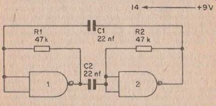
The circuit diagram of a CMOS equivalent of a conventional discrete multivibrator is shown in Figure 3. Resistors R1 and R2 are used to bias the inverters as linear amplifiers, and the two capacitors provide the cross coupling.
FIG.3 Basic conventional 1 kHz astable multivibrator
This circuit can be simplified slightly by using direct coupling between inverter 1 and inverter 2. This does away with the need for the coup ling capacitor which was formerly used here, and it also obviates the need for the bias resistor for inverter 2 (see Figure 4).
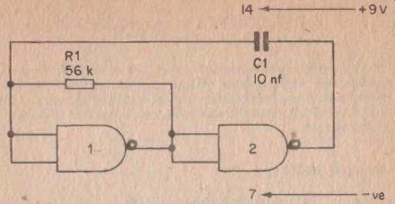
FIG. 4 Simplified 1 kHz astable circuit
The circuit operates in the following manner. When the supply is initially connected the output of one gate will go to the high state while the other will go to the low state. Which of these states the circuit assumes is unpredictable since it depends upon the characteristics of the two gates. For the sake of this explanation we will assume that inverter I has a high output, and inverter 2 has a low output.
C1 will begin to charge up from the high output of inverter 1 via R1. After a length of time which is determined by the values given to R1 and C1, the voltage across C1, and thus also at the input of inverter 1, will reach the transfer voltage of inverter I. This results in the output of inverter 1 going low, and in doing so drives the input of inverter 2 low. This causes the previously low output of inverter 2 to go high. As this occurs C1 is discharged into the inverters.
Now C1 starts to charge up from the negative supply through R1, which is connected to the now low output of inverter 1. As C1 charges up, the voltage at the inverter 1 will gradually fall, and after a time determined by the time constant of C1 and R1, the transfer voltage of the gate will be reached. This drives the output of inverter 1 high, which in turn takes the input to inverter 2 high. This causes the output of inverter 2 to go low, and C1 is again discharged through the inverters as this all happens.
The circuit operation then commences at the beginning again with C1 charging via R1 from the high output of inverter 1. The circuit thus continually oscillates with antiphase squarewave outputs being produced at the outputs of the inverters.
This circuit has several advantages over a conventional discrete component multivibrator. As we have already seen, it has only two frequency determining components rather than the usual four. Also it can be made to operate over a very wide frequency range. At the low frequency end of the spectrum this is due to the very high input impedances of the inverters. This enables very high values to be used for R1, which when used in conjunction with a high value for C1 enables an operating frequency of less than one cycle per hour to be attained. On the other hand the circuit will operate reliably using a capacitor of a few pF in value and a resistor of a few K ohms. Operating frequencies into the Meg Hertz region are then possible.
Another advantage of this circuit is its low level of current consumption. At frequencies within the audio frequency spectrum, or below it, the circuit has a current consumption of less than 500 microamps from a 9 volt supply.
One drawback of the circuit is that the frequency of operation tends to vary with fluctuations in the supply voltage, and it also varies somewhat between individual circuits built to the same design due to variations in the transfer voltages of individual inverters. However, in most applications this is of no great significance.
Squarewave Generator
Perhaps the most obvious use for an astable multivibrator is as the basis of an audio squarewave generator. The circuit diagram of such a unit is shown in Figure 5.
This is basically just the circuit which was described in the previous section, except that the timing capacitor is actually three switched components, and the timing resistance has been made variable. The three switched capacitors provide the unit with three ranges, the output frequency being variable over these ranges by means of VR I . The three ranges are as follows:
Range 1 20Hz to 200 hz
Range 2 200 hz to 2kHz
Range 3 2kHz to 20kHz
Thus the unit covers the whole of the audio frequency spectrum. There is actually a slight overlap between ranges so that any variations in frequency coverage between individual units should not create any gaps in the frequency coverage.
As is common to all astable multivibrator circuits, the output waveform of this circuit is not a very good squarewave, with severe rounding at the top of the leading edge of the waveform. This is illuminated by using a third inverter as a buffer at the output. The multivibrator chops this from one state to the other with a high quality squarewave being produced at the output. VR2 is the output level control, and the maximum peak to peak output voltage of the unit is fractionally less 9 determining components rather than the usual four. Also it can be made to operate over a very wide frequency range. At the low frequency end of the spectrum this is due to the very high input impedances of the inverters. This enables very high values to be used for R1 , which when used in conjunction with a high value for C1 enables an operating frequency of less than one cycle per hour to be attained. On the other hand the circuit will operate reliably using a capacitor of a few pF in value and a resistor of a few K ohms. Operating frequencies into the megahertz region are then possible.
Another advantage of this circuit is its low level of current consumption. At frequencies within the audio frequency spectrum, or below it, the circuit has a current consumption of less than 500 microamps from a 9 volt supply.
One drawback of the circuit is that the frequency of operation tends to vary with fluctuations in the supply voltage, and it also varies somewhat between individual circuits built to the same design due to variations in the transfer voltages of individual inverters. However, in most applications this is of no great significance.
Squarewave Generator
Perhaps the most obvious use for an astable multivibrator is as the basis of an audio squarewave generator. The circuit diagram of such a unit is shown in Figure 5.
This is basically just the circuit which was described in the previous section, except that the timing capacitor is actually three switched components, and the timing resistance has been made variable. The three switched capacitors provide the unit with three ranges, the output frequency being variable over these ranges by means of VR1. The three ranges are as follows: -
Range 1 20Hz to 200Hz
Range 2 200Hz to 2kHz
Range 3 2kHz to 20kHz
Thus the unit covers the whole of the audio frequency spectrum. There is actually a slight overlap between ranges so that any variations in frequency coverage between individual units should not create any gaps in the frequency coverage.
As is common to all astable multivibrator circuits, the output waveform of this circuit is not a very good squarewave, with severe rounding at the top of the leading edge of the waveform. This is illuminated by using a third inverter as a buffer at the output. The multivibrator chops this from one state to the other with a high quality squarewave being produced at the output. VR2 is the output level control, and the maximum peak to peak output voltage of the unit is fractionally less
FIG.5 Wide range squarewave generator
than the power supply voltage.
A dial calibrated in frequency can be marked around the control knob of VR1 using any of the usual methods for output frequency determination. Provided C1 to C3 have reasonably low tolerances, say 5% or less, a single 20 to 200 scale will suffice for all three ranges (multiply by ten for range 2, and by 100 for range 3).
The pin identification diagram for the 4001 and 4011 devices is shown in Figure 6. These both use the same leadout arrangement.
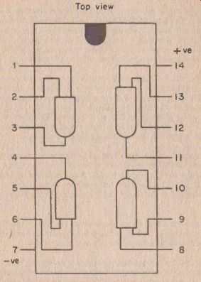
FIG. 6 Details of the pinning of the 4001 and 4011 I.C.s
Water Level Alarm
One of the most widespread uses of astable multivibrators is in the generation of alarm signals of various types. The squarewave output is very strident and is not easily missed.
11 than the power supply voltage.
A dial calibrated in frequency can be marked around the control knob of VR1 using any of the usual methods for output frequency determination. Provided C1 to C3 have reasonably low tolerances, say 5% or less, a single 20 to 200 scale will suffice for all three ranges (multiply by ten for range 2, and by 100 for range 3).
The pin identification diagram for the 4001 and 4011 devices is shown in Figure 6. These both use the same leadout arrangement.
FIG. 6 Details of the pinning of the 4001 and 4011 I.C.
Water Level Alarm
One of the most widespread uses of astable multivibrators is in the generation of alarm signals of various types. The squarewave output is very strident and is not easily missed.
Ordinary CMOS gates are unable to provide sufficient output power to properly drive even a miniature loudspeaker, and it is necessary to use a stage of amplification between the output of the tone generator and the loudspeaker.
Figure 7 shows the circuit diagram of a water level detector which uses a CMOS multivibrator. This type of alarm can be used in various applications, such as for monitoring the water level in the bilges of a boat, and sounding a warning if the level rises above a predetermined point. They also have household applications, and can be used as rain alarms, or to indicate when the water level in a bath has reached the required level.
Basically the circuit consists of an astable driving a common emitter transistor stage via an inverter/buffer stage. R3 limits the base current to Tr1 to a safe level. The loudspeaker forms the collector load for Tr1, and in consequence a large pulse of current is passed by the speaker each time the output of the inverter/buffer goes high. This causes a loud audio tone to be emitted from the speaker.
The timing resistor of the multivibrator is not directly connected between the input and output of inverter 1, but is connected via a sensor. The sensor is a simple device that has two electrodes which are arranged so that they are bridged by water when it reaches the required level (or rain drops fall on the sensor). The sensor normally acts as an open circuit, and so it does not complete the bias circuit of inverter 1 with the circuit failing to oscillate as a result.
When the sensor contacts are bridged by the water, the sensor will exhibit a relatively low impedance as the water will provide a conductive path between the two electrodes. This completes the bias circuit and the alarm will sound, and will continue to do so for as long as power is applied to the circuit and the sensors electrodes are bridged by water.
It is worth noting that although pure water is a poor conductor of electricity, rain, tap, and sea water contain sufficient impurities to produce a low impedance path between the electrodes.
R2 is required for two reasons. Firstly, it is not a good idea to leave an inverter's input open circuit, as would otherwise be the case here when the alarm is not sounding. This is because it will tend to pick up stray interference which would cause a continuous noise to be produced from the speaker. It would also result in wasted power.
Secondly, this resistor ensures that when the alarm is not operating, no current flows through the speaker. By taking the input of inverter 1 high under static conditions R2 ensures that the output of inverter 3 is low, and Tr1 is cut off. If the circuit was to latch in the opposite state (inverter 3 output high) a considerable quiescent output current would flow.
Ordinary CMOS gates are unable to provide sufficient output power to properly drive even a miniature loudspeaker, and it is necessary to use a stage of amplification between the output of the tone generator and the loudspeaker.
Figure 7 shows the circuit diagram of a water level detector which uses a CMOS multivibrator. This type of alarm can be used in various applications, such as for monitoring the water level in the bilges of a boat, and sounding a warning if the level rises above a predetermined point. They also have household applications, and can be used as rain alarms, or to indicate when the water level in a bath has reached the required level.
Basically the circuit consists of an astable driving a common emitter transistor stage via an inverter/buffer stage. R3 limits the base current to Tr1 to a safe level. The loudspeaker forms the collector load for Tr1 , and in consequence a large pulse of current is passed by the speaker each time the output of the inverter/buffer goes high. This causes a loud audio tone to be emitted from the speaker.
The timing resistor of the multivibrator is not directly connected between the input and output of inverter 1, but is connected via a sensor. The sensor is a simple device that has two electrodes which are arranged so that they are bridged by water when it reaches the required level (or rain drops fall on the sensor). The sensor normally acts as an open circuit, and so it does not complete the bias circuit of inverter 1 with the circuit failing to oscillate as a result.
When the sensor contacts are bridged by the water, the sensor will exhibit a relatively low impedance as the water will provide a conductive path between the two electrodes. This completes the bias circuit and the alarm will sound, and will continue to do so for as long as power is applied to the circuit and the sensors electrodes are bridged by water.
It is worth noting that although pure water is a poor conductor of electricity, rain, tap, and sea water contain sufficient impurities to produce a low impedance path between the electrodes.
R2 is required for two reasons. Firstly, it is not a good idea to leave an inverter's input open circuit, as would otherwise be the case here when the alarm is not sounding. This is because it will tend to pick up stray interference which would cause a continuous noise to be produced from the speaker. It would also result in wasted power.
Secondly, this resistor ensures that when the alarm is not operating, no current flows through the speaker. By taking the input of inverter 1 high under static conditions R2 ensures that the output of inverter 3 is low, and Tr1 is cut off. If the circuit was to latch in the opposite state (inverter 3 output high) a considerable quiescent output current would flow.
FIG. 7 Water level alarm circuit
The circuit has a static current consumption of only a minute fraction of a micro -amp, and it is economically viable to power the unit from a battery even if it is to be used for very prolonged periods. The current consumption when the alarm is operating is something in the region of 18 mA.
Unless the leads to the sensor are exceptionally long, or pass close to a mains lead or some similar source of electrical interference, there is no need for them to be screened. If this cable does need to be of the screened variety, a single screened type can be used (outer to R1, inner to inverter 1 input).
Christmas Tree Lights Flasher
Several useful gadgets can be made using a multivibrator to drive a relay, and a popular example is a Christmas Tree Lights Flasher. This will provide a much more regular flashing rate than can be obtained by using a bi-metal type flashing bulb, and the flashing rate can also be made variable. The circuit diagram of this device appears in Figure 8.
The two inverters are connected as a low frequency astable circuit, and the operating frequency of this is variable over a range of about 0.5 to 1.5 Hz by means of R1. The output of inverter 2 drives common emitter amplifier Tr2, via R3. R3 is a current limiting resistor.
Tr1 has the relay coil as its collector load, and the relay will be energized when the output of inverter 2 is high. The relay will be off when the output of inverter 2 is low. A single set of relay contacts (either normally closed or normally open ones) are used to control the lights.
These will therefore switch on and off at a rate determined by the setting of R1.
D1 is a protective diode, and this is needed to protect the circuit against the high reverse voltage which is developed across the relay coil as the power to the circuit is switched off. This voltage is generated by the magnetic lines of force quickly decaying and cutting through the relay coil. Because of the speed at which this magnetic force dies away, quite a high voltage can be produced, but it is at a high impedance. D1, in effect, shorts out this voltage, and is protected against passing an excessive current by the high source resistance of the signal.
D1 should not be omitted from the circuit as this voltage spike is quite capable of destroying both the I.C. and Tr1.
The circuit has a static current consumption of only a minute fraction of a micro-amp, and it is economically viable to power the unit from a battery even if it is to be used for very prolonged periods. The current consumption when the alarm is operating is something in the region of 18 mA.
Unless the leads to the sensor are exceptionally long, or pass close to a mains lead or some similar source of electrical interference, there, is no need for them to be screened. If this cable does need to be of the screened variety, a single screened type can be used (outer to R1, inner to inverter 1 input).
Metronome
A low frequency astable multivibrator can be used as the basis of a very simple metronome, and the circuit diagram of such a metronome appears in Figure 9.
FIG. 8 Christmas tree lamps flasher
FIG. 9 Metronome circuit
Inverters 1 and 2 are used to form the astable circuit, which has a continuously variable frequency range of approximately 0.5 to 5Hz. The frequency is adjusted by means of VR1.
The output of the multivibrator is fed to an inverter/buffer stage, and the output of this drives a single transistor output stage. R2 is the base bias resistor for the output transistor (Tr1), but this has a very high value and it does not bias Tr1 into class A operation. It only takes T r1 just beyond the threshold of conduction, and this stage actually works in the class B mode.
When the output of inverter 3 goes positive, a brief positive pulse is fed to the base of T r1 by way of C2, and this turns Tr1 hard on for the duration of the pulse. This causes a brief but fairly large pulse of current to be passed by the speaker which forms the collector load for T r1. C2 has purposely been given a fairly low value so that the duration of this pulse is short, and a click of a fairly high pitch is produced from the speaker. This makes a very good simulation of the click produced by a conventional metronome. Of course, a click is produced each time the output of inverter 3 goes high, and this results in about 40 to 300 clicks being produced each minute, the required rate being set using VR1. A beat rate of 40 to 300 per minute covers all normal musical requirements.
When the output of inverter goes negative, no significant audio output is produced. This is because the output transistor will be cut off by the negative voltage pulse which is supplied to its base. Being biased into class B operation, Tr1 is virtually cut off anyway, and the negative pulses therefore have no real effect on the output stage.
This gives the unit a very low average current consumption, and the current consumption of the prototype is only about 2 mA.
A dial calibrated in beats per minute should be marked around the control knob of VR1, and this is quite simple to accomplish. The range of operating frequencies is so low that it is quite easy to count the number of beats per minute produced with VR1 at various settings.
The dial is then calibrated at these settings.
It is advisable to try to find settings that correspond to beat rates that arc divisible by five or ten, as a dial calibrated at points such as 40, 70, 100, 150 etc., will look more neat than one calibrated at points such as 42, 7 1 ,9 8 , 153 etc. Unfortunately, the only way to find the desired calibration points is by trial and error, and this is likely to be time consuming. It is possible to save a certain amount of time by counting the number of beats in a 15 second period and then multiplying this by four to find the numbers of beats per minute, rather than by doing a straight forward minute count. This should not be done at the lower calibration points because accuracy could suffer as a result of this.
Transistor Tester
Most transistor testers arc designed to test a transistor which has been removed from its circuit, or to test it prior to being connected into circuit. Provided one does not want to actually measure the gain or some other parameter of the device under test, it is usually quite possible to test the device while it is connected into circuit. The circuit diagram of such a 'Go' - 'No Go' tester is shown in Figure 10.
The idea of this circuit is simply to apply a periodic forward bias to the base of the transistor while monitoring its collector current. The bias signal is obtained from the output of an inverter which is driven from a low speed astable circuit. The collector current is monitored by a light emitting diode indicator (D1).
If we consider the circuit first in the p.n.p. testing mode. When the output of the inverter is high, the base of the transistor will be at virtually the same potential as its emitter, and it will therefore not conduct. The L.E.D. will not light up since it will receive no significant current.
When the output of inverter 3 goes low, a large forward bias is applied to the test transistor which should, in consequence, be biased into saturation. A large current will flow through D1 which will light up.
Thus if the transistor under test is a good operational device, upon connecting the test prods to it, the L.E.D. indicator should flash on and off (at a rate of around 1 Hz).
If the test transistor is a closed circuit device, then of course the bias will have no effect, and DI will be on all the time. If the transistor is an open circuit device, then D1 will not come on at all.
The circuit operates in precisely the same manner when it is switched to the n.p.n. mode, except that the transistor is cut off when the output of inverter 3 is low, and saturated when it is high. The unit is used in exactly the same way whichever mode it is in.
It should perhaps be pointed out that this circuit is not fool -proof, and it can give misleading results. This is because the base and emitter of the test transistor are not genuinely short circuited together when the device is supposed to be cut off. It is therefore just possible that circuit resistances could bias the transistor on. It is also possible that circuit resistances could supply a path for the L.E.D. current flow. Thus the L.E.D. could be continually on even though the test transistor is sound.
It is also possible that the L.E.D. could fail to come on even if the transistor is operational. This could occur if it has a low resistance in its base - emitter circuit, as the potential divider effect between this and R2 of the tester could produce a base - emitter voltage of insufficient level to turn the transistor on.
Transistor Tester
Most transistor testers are designed to test a transistor which has been removed from its circuit, or to test it prior to being connected into circuit. Provided one does not want to actually measure the gain or some other parameter of the device under test, it is usually quite possible to test the device while it is connected into circuit. The circuit diagram of such a 'Go' - 'No Go' tester is shown in Figure 10.
The idea of this circuit is simply to apply a periodic forward bias to the base of the transistor while monitoring its collector current. The bias signal is obtained from the output of an inverter which is driven from a low speed astable circuit. The collector current is monitored by a light emitting diode indicator (Dl).
If we consider the circuit first in the p.n.p. testing mode. When the output of the inverter is high, the base of the transistor will be at virtually the same potential as its emitter, and it will therefore not conduct. The L.E.D. will not light up since it will receive no significant current.
When the output of inverter 3 goes low, a large forward bias is applied to the test transistor which should, in consequence, be biased into saturation. A large current will flow through D1 which will light up.
Thus if the transistor under test is a good operational device, upon connecting the test prods to it, the L.E.D. indicator should flash on and off (at a rate of around 1 Hz).
If the test transistor is a closed circuit device, then of course the bias will have no effect, and D1 will be on all the time. If the transistor is an open circuit device, then Dl will not come on at all.
The circuit operates in precisely the same manner when it is switched to the n.p.n. mode, except that the transistor is cut off when the output of inverter 3 is low, and saturated when it is high. The unit is used in exactly the same way whichever mode it is in.
It should perhaps be pointed out that this circuit is not fool-proof, and it can give misleading results. This is because the base and emitter of the test transistor are not genuinely short circuited together when the device is supposed to be cut off. It is therefore just possible that circuit resistances could bias the transistor on. It is also possible that circuit resistances could supply a path for the L.E.D. current flow. Thus the L.E.D. could be continually on even though the test transistor is sound.
It is also possible that the L.E.D. could fail to come on even if the transistor is operational. This could occur if it has a low resistance in its base - emitter circuit, as the potential divider effect between this and R2 of the tester could produce a base - emitter voltage of insufficient level to turn the transistor on.
FIG. 10 Transistor tester circuit.
Results obtained with this tester should not, therefore, be regarded as being infallible. When testing ordinary low level transistor stages the device is unlikely to produce erroneous results, since the necessary low circuit resistances will not be present. Caution should be exercised when testing power devices though.
It can be said in favor of this tester that its usefulness is disproportion ate to its very low cost.
One final point is that no power should be connected to the circuit in which the test transistor is employed.
Low Power Pilot Light
It is advisable to fit a pilot light to any item of electronic equipment, such as signal generators, and electronic voltmeters, where it is easy to inadvertently leave the equipment switched on. This is especially so in the case of battery operated equipment, where leaving the equipment turned on will prove to be rather expensive.
Fitting a pilot light to battery operated equipment does represent something of a problem since in order to be worthwhile, the pilot light must consume very little battery current. Otherwise it could well consume more power than is saved by always remembering to switch the equipment off.
Light emitting diodes currents, but in order to provide a really noticeable light level they really need to consume something in the region of 10 mA. This is more than is consumed by many pieces of battery operated equipment.
One way of reducing the current consumption of an L.E.D. pilot light is to use a pulsing technique. For example, if during one second periods the L.E.D. is only briefly turned on for (say) 0.1 seconds, then the average current consumption will be reduced by 90%. In this way the L.E.D. can be made to produce a very noticeable pilot light with a current consumption of only 1 mA or even less.
Furthermore, the fact that the light is flashing will tend to make it more noticeable than one which is on continuously. Thus, although it uses less power, a flashing pilot light is more efficient.
The low current consumption of a CMOS I.C. makes it the ideal basis for a low power pilot light, and the circuit diagram of such a unit appears in Figure 11. Inverters 1 and 2 are used as an astable multi -vibrator, and inverter 3 is used as a buffer stage which drives the L.E.D. indicator.
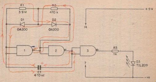
FIG. 11 The low power pilot light
It will be seen from Figure 11 that the astable circuit is a modified version of the type used in the previous circuits. The timing resistor has been divided into two separate components ( R1 and R2), and steering diodes have been added (D1 and D2).
In effect, these diodes short out one resistor when C1 is charging from the positive supply, and the other resistor when it is charging from the negative supply. It charges from the positive supply via R1, and from the negative supply by way of R2. As R1 has a much higher value than R2, the output of inverter 2 is in the high state longer than it is in the low state. This must be the case since it will take the voltage across C1 longer to reach the transfer voltage of inverter 1 when C1 is charging through the higher resistance.
An inverter in interposed between the output of inverter 2 and the L.E.D. circuit, and so the voltage here is low for longer periods than it is high. The circuit operates at a frequency of about 1 Hz, and so D1 is briefly switched on at approximately 1 second intervals.
The average current consumption of the prototype circuit was measured at about 900 micro-amps from a 9 volt supply.
Second Timer
This is a simple device which produces an audio tone shortly after a switch is operated. The delay is variable from zero to about ten seconds. Simple timers such as this can be used in T.V. type quiz games where there is a time limit during which the question must be answered if one is to score. They can also be employed in other games, such as lightning chess or draughts, and there must be many other possible uses for such devices.
The circuit diagram of the timer is shown in Figure 12. Inverters 1 and 2 arc used as a straight forward audio frequency astable circuit which actually operates at a frequency of about 500 Hz.
The output of the astable is fed to a common emitter amplifier via a pulse enabling circuit. This merely consists of one of the NAND gates of a 4011 I.C., and the way in which this operates is very simple.
When the control input of the gate is in the low state, input signals at the signal input will have no effect on the output. This is because the output of a NAND gate is high unless both the inputs are high, in which case the output takes up the low state. Thus if the control input is low, the state of the signal input is irrelevant as the output will be high.
Therefore, when the control input of gate 3 is low, its output will be high and Tr1 will be cut off. No sound will be produced from the speaker. When S1 is opened, the voltage at the control input of gate 3 will begin to rise as C3 charges up via VR1 . When the voltage across C3 goes above the transfer voltage of the enabling gate, the output state of this gate will be dependent upon the signal at its other input.
0 - 10 Second Timer
This is a simple device which produces an audio tone shortly after a switch is operated. The delay is variable from zero to about ten seconds. Simple timers such as this can be used in T.V. type quiz games where there is a time limit during which the question must be answered if one is to score. They can also be employed in other games, such as lightning chess or draughts, and there must be many other possible uses for such devices.
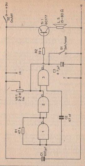
FIG.12
0-10 sec. timer. Only use IC 4011 in this circuit FIG. 12 0-10 sec. timer.
Only use IC 4011 in this circuit
The circuit diagram of the timer is shown in Figure 12. Inverters 1 and 2 are used as a straight forward audio frequency astable circuit which actually operates at a frequency of about 500 Hz.
The output of the astable is fed to a common emitter amplifier via a pulse enabling circuit. This merely consists of one of the NAND gates of a 4011 I.C., and the way in which this operates is very simple.
When the control input of the gate is in the low state, input signals at the signal input will have no effect on the output. This is because the output of a NAND gate is high unless both the inputs are high, in which case the output takes up the low state. Thus if the control input is low, the state of the signal input is irrelevant as the output will be high.
Therefore, when the control input of gate 3 is low, its output will be high and T r1 will be cut off. No sound will be produced from the speaker. When S1 is opened, the voltage at the control input of gate 3 will begin to rise as C3 charges up via VR1. When the voltage across C3 goes above the transfer voltage of the enabling gate, the output state of this gate will be dependent upon the signal at its other input When the signal input is low the output is high, and the output is low when the signal input is high. Tr1 will then be pulsed on and off and an audio tone will be produced from the speaker.
The time taken for the voltage across C3 to reach the transfer voltage of gate 3 depends upon the setting of VR1. When this is adjusted for zero resistance there is zero delay. This can be increased to a maximum delay of about ten seconds with V R1 at maximum resistance. Note, however, that the maximum time delay will vary somewhat between individual circuits due to the wide tolerances of certain components (C3 in particular).
The circuit is reset by closing S1 which then discharges C3 and thus cuts off the audio tone. A new timing period is started by opening S1 again.
A 4001 I.C. is not suitable for use in this circuit since gate 3 is not used as an inverter, and the NOR gates of a 4001 would not provide the required circuit action. Although in this circuit explanation the inputs of gate 3 were termed the signal and control gates, the inputs to this gate can be connected either way round. Whichever one is connected to C3 becomes the control input and the one connecting to gate 2 becomes the signal input.
Pulsed Tone Generator
Two circuits using audible alarms have been described so far, and these both use simple continuous tone circuits. A more effective alarm can be produced by either having a tone of varying pitch (such as police car sirens), or by using an intermittent tone (as do many burglar alarm systems for instance). The circuit shown in Figure 13 is of the latter type.
Here inverters 1 and 2 form a low frequency astable having an operating frequency of about 1 Hz, and inverters 3 and 4 are used as an astable tone generator operating at a frequency of very approximately 800 Hz.
Gate 3 is not used as a straight forward inverter, but is used as an enabling gate.
When the output of the L.F. astable is low, the tone generator will obviously be blocked and will be unable to oscillate. When output of the L.F. astable is high, gate 3 will function as an ordinary inverter and the tone generator will function normally. Thus the low frequency astable switches the tone generator on and off at a rate of about 1 Hz, and an intermittent output is produced.
Gate 3 is used as the control gate rather than gate 4, as with the alter native method the output of the tone generator would be high when the circuit was in the muted state. This would turn Tr1 on and would result in increased current consumption.
When the signal input is low the output is high, and the output is low when the signal input is high. T r1 will then be pulsed on and off and an audio tone will be produced from the speaker.
The time taken for the voltage across C3 to reach the transfer voltage of gate 3 depends upon the setting of VR1. When this is adjusted for zero resistance there is zero delay. This can be increased to a maximum delay of about ten seconds with VR1 at maximum resistance. Note, however, that the maximum time delay will vary somewhat between individual circuits due to the wide tolerances of certain components (C3 in particular).
The circuit is reset by closing S1 which then discharges C3 and thus cuts off the audio tone. A new timing period is started by opening S1 again.
A 4001 I.C. is not suitable for use in this circuit since gate 3 is not used as an inverter, and the NOR gates of a 4001 would not provide the required circuit action. Although in this circuit explanation the inputs of gate 3 were termed the signal and control gates, the inputs to this gate can be connected either way round. Whichever one is connected to C3 becomes the control input and the one connecting to gate 2 becomes the signal input.
Pulsed Tone Generator
Two circuits using audible alarms have been described so far, and these both use simple continuous tone circuits. A more effective alarm can be produced by either having a tone of varying pitch (such as police car sirens), or by using an intermittent tone (as do many burglar alarm systems for instance). The circuit shown in Figure 13 is of the latter type.
Here inverters 1 and 2 form a low frequency astable having an operating frequency of about 1 Hz, and inverters 3 and 4 are used as an astable tone generator operating at a frequency of very approximately 800 Hz.
Gate 3 is not used as a straight forward inverter, but is used as an enabling gate.
When the output of the L.F. astable is low, the tone generator will obviously be blocked and will be unable to oscillate. When output of the L.F. astable is high, gate 3 will function as an ordinary inverter and the tone generator will function normally. Thus the low frequency astable switches the tone generator on and off at a rate of about 1 Hz, and an intermittent output is produced.
Gate 3 is used as the control gate rather than gate 4, as with the alternative method the output of the tone generator would be high when the circuit was in the muted state. This would turn Tr1 on and would result in increased current consumption.
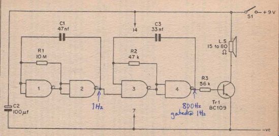
FIG.13 Pulsed tone generator circuit (use only 4011)
Pulsed Output Timer
It is a simple matter to modify the pulsed tone generator circuit to produce a simple timer of the type described earlier, but with a pulsed output of course. The circuit diagram of this device appears in Figure 14.
Here gate 1 is used as an enabling gate, and the control input is normally held in the low state by S1. This prevents the low frequency astable from oscillating, and causes its output to be in the low state. This causes the tone generator astable to also be blocked, and so no output is produced from the speaker.
When S1 is opened, C4 begins to charge up via VR1, and when the potential across C4 exceeds the transfer voltage of gate 1, the low frequency astable will turn on. The pulsed tone generator then functions normally with an intermittent tone being emitted from the speaker.
BISTABLE CIRCUITS
The bistable is the simplest of the multivibrator family, but it is not used nearly as much as the astable type. In fact it is rarely encountered in circuits for the amateur, but it can be very useful on occasions.
A bistable can be very easily constructed from a couple of CMOS inverters, and only two resistors and two push button switches are needed in addition to the inverters. The circuit diagram of a basic CMOS inverter is shown in Figure 15.
In this type of circuit one output is low and the other is high. The circuit therefore has two stable states, and it is from this that i t derives its name.
Which output goes high and which goes low when the power is initially connected to the circuit depends upon unpredictable parameters. It is mainly dependent upon the operating speeds of the inverters. Assume for example, that inverter 1 is capable of faster operation than inverter 2. When the supply is turned on, the inputs of both inverters will be low, and the outputs will try to go high. The output of inverter 1 will go high at a faster rate than the output of inverter 2, and a rising voltage will therefore be coupled from the output of inverter 1 to the input of inverter 2 via R1. This voltage will have the effect of holding inverter 2 output in the low state while the output of inverter 1 goes high. The circuit then rests in this state.
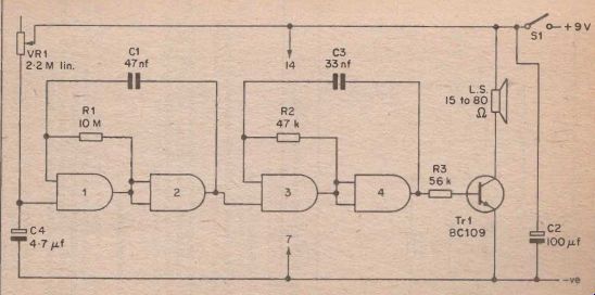
FIG. 14 Pulsed output 0-10 second timer (use only 4011).
The circuit can be made to take up the opposite state by momentarily operating push button switch S2. This takes the input of inverter 2 low and its output to go high. This takes the input of inverter 1 high as this is connected to the output of inverter 2 via R2. In consequence the output of inverter 1 goes high.
Even when S2 is released, the circuit will remain in its new state. It can be returned to its original state by operating S1 momentarily.
This circuit forms a sort of simple electronic memory, because once it is set in a certain state it remains in that state, and could be said to remember that state. It is also sometimes referred to as a latch, since once set in a certain state it latches in that state.
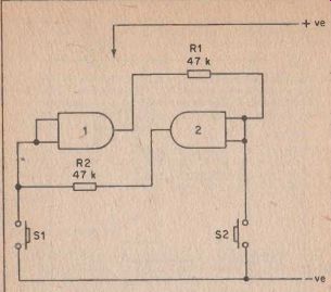
FIG. 15 Basic bistable multivibrator circuit
Switch Precedence Indicator
One popular use of bistable circuits is in switch precedence indicators.
This is the type of device which is used in T.V. type quizzes where the lust person to press his or her switch has the first opportunity to answer the question. The purpose of the device is to render the un-operated switches inoperative the instant one of the switches is closed.
Similar games are often played in the home, and such a device can be used when playing games such as snap, the well known card game.
The circuit diagram of a simple switch precedence indicator is shown the output of inverter 1 goes high.
Even when S2 is released, the circuit will remain in its new state. It can be returned to its original state by operating S1 momentarily.
This circuit forms a sort of simple electronic memory, because once it is set in a certain state it remains in that state, and could be said to remember that state. It is also sometimes referred to as a latch, since once set in a certain state it latches in that state.
Switch Precedence Indicator
One popular use of bistable circuits is in switch precedence indicators.
This is the type of device which is used in T.V. type quizzes where the first person to press his or her switch has the first opportunity to answer the question. The purpose of the device is to render the un-operated switches inoperative the instant one of the switches is closed.
Similar games are often played in the home, and such a device can be used when playing games such as snap, the well known card game.
The circuit diagram of a simple switch precedence indicator is shown in Figure 16.
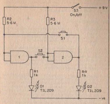
FIG. 16 Circuit diagram of the switch precedence ind.
Both lamps are off when neither of the switches are closed, since the input of each inverter will be taken high by its bias resistor (R2 and R3). The output of each inverter will therefore be low, and neither L.E.D. indicator will be supplied with any current.
If one of the push button switches is operated, say S1, then the appropriate indicator lamp will come on. In this case it will be D1 that will come on, as the input of inverter I will be taken low by being connected to the low output of inverter 2.
If S2 is now operated, D2 will not come on because the output of inverter 1 is high, and closing S2 will merely keep inverter 1 input in its present state. Thus when a push button is operated the appropriate lamp will come on, and the other push button is blocked, and will have no effect on the circuit.
The circuit is reset ready for a new round to commence by simply releasing the push buttons.
FIG. 16 Circuit diagram of the switch precedence ind.
Both lamps are off when neither of the switches are closed, since the input of each inverter will be taken high by its bias resistor (R2 and R3). The output of each inverter will therefore be low, and neither L.E.D. indicator will be supplied with any current.
If one of the push button switches is operated, say S1, then the appropriate indicator lamp will come on. In this case it will be Dl that will come on, as the input of inverter 1 will be taken low by being connected to the low output of inverter 2.
If S2 is now operated, D2 will not come on because the output of inverter 1 is high, and closing S2 will merely keep inverter 1 input in its present state. Thus when a push button is operated the appropriate lamp will come on, and the other push button is blocked, and will have no effect on the circuit.
The circuit is reset ready for a new round to commence by simply releasing the push buttons.
This circuit, together with the simple timer described earlier, could form the basis of a simple reaction testing game. The timer would be set to give a delay of a few seconds and then it would be started. The two players would each have a push button switch, and the winner would be the person who operated his or her switch the most quickly once the audible alarm had begun to sound.
Heads Or Tails Simulator
Another popular type of novelty circuit which often employs a bistable circuit in some form or other is a heads or tails simulator. This kind of circuit is designed to electronically simulate the tossing of a coin. The circuit diagram of such a device appears in Figure 17.
Inverters 1 and 2 are connected as an astable circuit having an operating frequency of a few hundred Hz. The other two inverters are connected as a simplified bistable circuit. The simplification is merely that inverter 3 output and inverter 4 input are directly connected together, rather than being connected by way of a resistor. This is possible as no input signal is applied to the input of inverter 4.
The input signal is coupled to the input of inverter 3 from the output of the astable circuit via SI. When the power is turned on the input of the bistable will be rapidly switched from the high to the low state by the astable multivibrator. The input and output of the bistable are in phase, and so the output will also be rapidly going from the high to the low state. Each time the output goes to the high state, D1 will briefly be pulsed on. It will be flashing on and off at such a fast rate though, that to a human observer the flashing will not be perceivable, and the lamp will appear to glow continuously.
When S1 is opened, the bistable will latch in whatever state it was in at the instant Si broke the continuity of the circuit. For instance, if the output of the bistable was in the high state when this occurred, its input will be held in the high position by the voltage which is coupled from output to input by R2. The L.E.D. indicator will therefore remain on.
The input of the bistable will similarly be held in the low state by this coupling if the output happened to be low at the instant S1 went open circuit, and in consequence the L.E.D. would go off.
The output from the astable circuit is a squarewave, and so the bistable is driven to the high and low states for equal lengths of time. It is therefore purely a matter of chance whether the indicator lamp remains on or switches off when S1 is operated. There is a 50-50 chance of it assuming any one of the two possible states, just as there is when one tosses a coin.
By classing the on state of the lamp 'heads', and the off state 'tails', the unit will thus simulate the tossing of a coin. Unlike some other heads This circuit, together with the simple timer described earlier, could form the basis of a simple reaction testing game. The timer would be set to give a delay of a few seconds and then it would be started. The two players would each have a push button switch, and the winner would be the person who operated his or her switch the most quickly once the audible alarm had begun to sound.
Heads Or Tails Simulator
Another popular type of novelty circuit which often employs a bistable circuit in some form or other is a heads or tails simulator. This kind of circuit is designed to electronically simulate the tossing of a coin. The circuit diagram of such a device appears in Figure 17.
Inverters 1 and 2 are connected as an astable circuit having an operating frequency of a few hundred Hz. The other two inverters are connected as a simplified bistable circuit. The simplification is merely that inverter 3 output and inverter 4 input are directly connected together, rather than being connected by way of a resistor. This is possible as no input signal is applied to the input of inverter 4.
The input signal is coupled to the input of inverter 3 from the output of the astable circuit via S1 . When the power is turned on the input of the bistable will be rapidly switched from the high to the low state by the astable multivibrator. The input and output of the bistable are in phase, and so the output will also be rapidly going from the high to the low state. Each time the output goes to the high state, 131 will briefly be pulsed on. It will be flashing on and off at such a fast rate though, that to a human observer the flashing will not be perceivable, and the lamp will appear to glow continuously.
When S1 is opened, the bistable will latch in whatever state it was in at the instant S1 broke the continuity of the circuit. For instance, if the output of the bistable was in the high state when this occurred, its input will be held in the high position by the voltage which is coupled from output to input by R2. The L.E.D. indicator will therefore remain on.
The input of the bistable will similarly be held in the low state by this coupling if the output happened to be low at the instant S1 went open circuit, and in consequence the L.E.D. would go off.
The output from the astable circuit is a squarewave, and so the bistable is driven to the high and low states for equal lengths of time. It is therefore purely a matter of chance whether the indicator lamp remains on or switches off when S1 is operated. There is a 5 0 -5 0 chance of it assuming any one of the two possible states, just as there is when one tosses a coin.
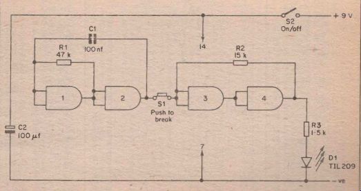
FIG. 17 Heads or toils simulator
By classing the on state of the lamp 'heads', and the off state 'tails', the unit will thus simulate the tossing of a coin. Unlike some other heads or tails circuits, this one requires no adjustment or experimentation with circuit values in order to obtain proper 50-50 operation.
Touch Switch
Touch switches seem to have become quite popular these days, and although this is probably mainly due to their novelty value rather than any practical advantage, they do have certain practical advantages over more conventional forms of switch. Probably the main one in most applications is that they can be designed to have no moving parts to wear out. This makes them as reliable and hard wearing as the main (electronic) part of the equipment they are controlling.
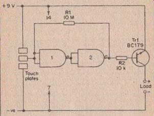
FIG. 18 The touch switch circuit The circuit diagram of a simple touch switch
using a CMOS bistable circuit is shown in Figure 18. This will provide on/off
switching for any piece of 9 volt battery operated equipment which does not
have a current consumption of more than 100 mA (the maximum operating current
for the BC179 transistor).
CMOS I.C.s are ideal for use in this particular application since they can easily provide the necessary very high input impedances, and they also consume no significant current when they are not driving a load.
The current consumption of this circuit in the off state is very low, being actually less than 1 micro-amp. There is subsequently no significant battery drain when the equipment is turned off, and the battery life should not be significantly less than if a mechanical switch were used.
Extra current is consumed when the unit is in the on state, this mainly being the base current to turn on Tr1. This is unavoidable, but the additional current consumed is less than 1 mA, and is likely to be of no significance in the majority of applications.
The circuit operates in the following manner. When the power is initially connected to the device the output of the bistable will go into the high condition. Tr1 is cut off and no power is applied to the load.
It is possible to alter the state of the bistable by touching the lower set of touch contacts. The resistance of the operators skin then takes the input of the bistable low, and the output of the bistable will then also go low. A base current is then applied to Tr1 which is biased into saturation, and virtually the full supply rail potential is supplied to the load.
The unit can be switched off again by touching the upper set of touch contacts. The input of the bistable is then connected to the positive supply by way of the skin resistance of the operator's finger, and in consequence both the input and output of the bistable take up the high condition. Tr1 is therefore cut off once again, with no significant current being supplied to the load.
R1 provides the necessary latching action by holding the input in what ever state it was in when the finger of the user is removed from the touch contacts. If necessary, the sensitivity of the circuit can be boosted by raising the value of R1. Resistors having values of more than 10 Megohms are not readily available, and so an increased value for R1 can only be obtained by adding two of more resistors in series to make up the required value.
R2 is needed in order to prevent Tr1 from passing an excessive base current. It also limits this current to an economical level. If the unit is being used to control a fairly high current load, say 25 mA or more, it is necessary to reduce the value of R2 to 1 k.
With a little ingenuity it should not be too difficult for the constructor to fabricate suitable touch contacts. A piece of stripboard can be used to make a very simple but effective touch plate, or an even better one can be etched from a piece of copper laminate board. Even three screws (Pan or Countersunk heads) mounted on the front panel of the main equipment could be used if they are suitable positioned.
Relay Version
In some applications the above circuit will not be suitable since it will only control 9 volt equipment which has a current consumption of 100 mA or less. If one wishes to control a higher power, or an alternating current, this can be accomplished by controlling the load via a relay having suitable contacts. In this way it is also possible to have change over switching, and such things as touch controlled wavechange switches become a possibility.
The circuit diagram of the relay version of the touch switch appears in Figure 19. This is the same as the original circuit except that Tr1 now have a relay as its collector load in place of the controlled equipment.
Protective diode, D1, has also been added.
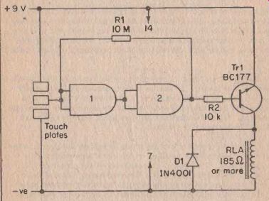
FIG. 19 Relay version of the touch switch
The relay can be any type which is suitable for 6 volt operation and has a coil resistance of 185 ohms or more, provided it has suitable contacts for its intended application, of course.
MONOSTABLE CIRCUITS
It is probably true to say that monostable circuits are among the least used of all electronic building blocks, as far as circuits for the amateur are concerned anyway. They are perhaps used more often now than they were a few years ago as monostable I.C.s such as the NE555 and 74121 have proved to be very versatile.
CMOS monostable devices are available, and an example is the 4047 I.C. However, when only a simple monostable is required it is usually
FIG. 20 Basic monostable circuit (only use I.C. 4001) easier and cheaper to
connect a couple of gates to form a monostable circuit. A simple monostable
can be produced from an inverter and a 2 input NOR gate. It is therefore possible
to make one (or two) from a 4001 I.C. The relevant circuit diagram is shown
in Figure 20.
The output of the inverter (gate 2) goes low when the power is initially connected to the circuit. This is because its input is taken high by R1.
The output of gate 1 will also be high since both the inputs are low. If either or both of the inputs of a NOR gate go high, the output will go low.
If a brief pulse is applied to the input of the circuit, this will momentarily take one input high and gate 1 output will therefore go low. This output pulse is fed via C1 to the input of the inverter, and in consequence the output of the monostable goes into the high state. This takes the second input of gate 1 high, and even if the other input now goes low, the output of gate 1 will remain in the high state.
C1 will begin to charge up via R1 the moment the output of gate 1 goes low, and eventually the voltage on C1 will reach the transfer voltage of gate 2, and its output will go low. This takes the second input of gate 1 low, and the circuit has now returned to its original and only stable state. It is from this that the name monostable is derived.
It is worth noting that even if the input to the circuit is taken positive for a long period, rather than just momentarily, the output waveform will be the same. This merely has the effect of holding the output of easier and cheaper to connect a couple of gates to form a monostable circuit. A simple monostable can be produced from an inverter and a 2 input NOR gate. It is therefore possible to make one (or two) from a 4001 I.C. The relevant circuit diagram is shown in Figure 20.
The input of the inverter (gate 2) goes low when the power is initially connected to the circuit. This is because its input is taken high by R1 . The output of gate 1 will also be high since both the inputs are low. If either or both of the inputs of a NOR gate go high, the output will go low.
If a brief pulse is applied to the input of the circuit, this will momentarily take one input high and gate 1 output will therefore go low. This output pulse is fed via C1 to the input of the inverter, and in consequence the output of the monostable goes into the high state. This takes the second input of gate 1 high, and even if the other input now goes low, the output of gate 1 will remain in the high state.
C1 will begin to charge up via R1 the moment the output of gate 1 goes low, and eventually the voltage on C1 will reach the transfer voltage of gate 2, and its output will go low. This takes the second input of gate 1 low, and the circuit has now returned to its original and only stable state. It is from this that the name monostable is derived.
It is worth noting that even if the input to the circuit is taken positive for a long period, rather than just momentarily, the output waveform will be the same. This merely has the effect of holding the output of gate 1 low if a positive input is still present at the end of the output pulse. When this input is eventually removed, then the circuit returns to its original state.
Thus a monostable multivibrator can be used to either lengthen a brief input pulse or shorten a long pulse. The length of the output pulse is controlled by the values given to C1 and R1. The length of the output pulse can be varied over very wide limits as it can be less than a micro -second to more than an hour. R1 can have a value of any where between about 10 k and many Megohms. C1 can be any value of more than a few pF. If C1 is an electrolytic type it has its positive terminal connected to R1.
With R1 at a value of 1.8 Meg the prototype gave an output pulse of approximately 1 second per mfd, but there is likely to be a fairly large variation between individual circuits in this respect. This is about the only real disadvantage of this very simple circuit.
Capacitance Meter
Most multimeters are equipped to measure wide ranges of voltage, current, and resistance, but few, if any, are capable of capacitance measurements. As a result of this, most electronics enthusiasts are unable to undertake capacitance measurements, and this must lead to many useable capacitors being discarded simply because their identification markings have become erased. Some means of testing capacitors is also very useful when one is engaged on servicing faulty equipment.
A capacitance meter is therefore a very useful piece of equipment to have in the workshop. A simple capacitance meter can be based on an astable and a monostable multivibrator, and it is possible to make one using a single CMOS I.C. as the only active device. The circuit diagram of such a unit is shown in Figure 21, and this uses a single 4001 I.C.
Gates 1 and 2 are connected as the astable circuit and gates 3 and 4 form the monostable multivibrator. The astable operates at a frequency of about 100 Hz, and its output is fed to the trigger input of the monostable. Thus one hundred times per second the monostable will produce an output pulse. The length of this output pulse is determined by the values of the timing components, and the timing capacitor under test. The timing resistor is one of the four resistors, R3 to R6, and is whichever one is switched into circuit by S1 .
By using four timing resistors the unit is able to provide four measuring ranges. These are as follows:-
Range 1 0 to 500 nF
Range 2 0 to 50 nF
Range 3 0 to 5 nF
Range 4 0 to 500 pF
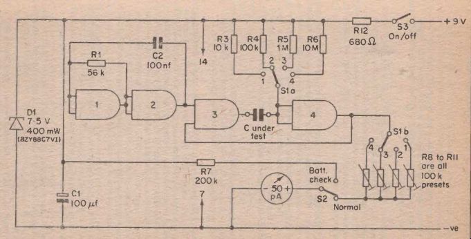
Fig. 21 The direct reading capacitance meter circuit (use only I.C. 4001)
The unit thus covers most normal amateur requirements.
The circuit value have been chosen so that the monostable acts as a pulse shortener. For instance, with the unit switched to Range 1 and a 500 nF test capacitor in circuit, the output pulse from the mono -stable will only be about half the length of the trigger pulse from the astable. Lower values of test capacitance will produce an even shorter monostable pulse length.
A voltmeter circuit consisting of M1 and one of the set of four preset resistors (R8 to R11) is connected at the output of the monostable.
Each time the output of the monostable goes high, a pulse of current will be fed to the meter. A constant string of pulses are generated when a test capacitor is connected to the unit, and the meter will respond to the average output voltage.
With a 500 nF test capacitor in circuit, R9 is adjusted to produce f.s.d. of the meter. If, for instance, a 100 nF capacitor is connected in place of the 500 nF one, the length of the output pulses will only be one-fifth of the previous duration. The rate at which the monostable is triggered is the same, and so the pulses still occur at the same frequency. Therefore the average voltage across the meter circuit will only be one -fifth of its original level, and the meter will read one-fifth f.s.d.
It will be apparent from this that there is a linear relationship between the meter reading and the value of the test capacitor. The unit thus functions very effectively as a linear reading capacitance meter.
On Range 2 the timing resistor is ten times the value of that used on Range 1. Only one-tenth of the previous test capacity is therefore needed to produce an identical meter reading. For example, 500 nF ' was needed to produce f.s.d. of the meter on Range 1 whereas only 50 nF will be needed on Range 2. In practice this is not quite the case since the tolerances of the timing resistors will prevent such a precise relationship from being obtained. In order to ensure that good accuracy is obtained on all four ranges, a different preset resistor for each range is provided in the meter circuit. This enables each range to be calibrated against a close tolerance capacitor.
An alternative approach is to use 1% tolerance components for R3 to R6, and a single calibration preset. The unit would then only need to be calibrated on one range, with good accuracy being automatically obtained on the other three ranges.
D1 and R12 are used to stabilize the supply voltage of the circuit, and this is essential if consistent and reliable results are to be obtained.
There are two reasons for this. Firstly, the frequency of the astable circuit will vary slightly with variations in supply rail potential. If it should speed up at all, then there will be more pulses applied to the meter in a given period of time, and increased meter readings will be The unit thus covers most normal amateur requirements.
The circuit value have been chosen so that the monostable acts as a pulse shortener. For instance, with the unit switched to Range 1 and a 500 nF test capacitor in circuit, the output pulse from the monostable will only be about half the length of the trigger pulse from the astable. Lower values of test capacitance will produce an even shorter monostable pulse length.
A voltmeter circuit consisting of Ml and one of the set of four preset resistors (R8 to R11) is connected at the output of the monostable.
Each time the output of the monostable goes high, a pulse of current will be fed to the meter. A constant string of pulses are generated when a test capacitor is connected to the unit, and the meter will respond to the average output voltage.
With a 500 nF test capacitor in circuit, R9 is adjusted to produce f.s.d. of the meter. If, for instance, a 100 nF capacitor is connected in place of the 500 nF one, the length of the output pulses will only be one- fifth of the previous duration. The rate at which the monostable is triggered is the same, and so the pulses still occur at the same frequency. Therefore the average voltage across the meter circuit will only be one-fifth of its original level, and the meter will read one-fifth f.s.d.
It will be apparent from this that there is a linear relationship between the meter reading and the value of the test capacitor. The unit thus functions very effectively as a linear reading capacitance meter.
On Range 2 the timing resistor is ten times the value of that used on Range 1. Only one-tenth of the previous test capacity is therefore needed to produce an identical meter reading. For example, 500 nF was needed to produce f.s.d. of the meter on Range 1 whereas only 50 nF will be needed on Range 2. In practice this is not quite the case since the tolerances of the timing resistors will prevent such a precise relationship from being obtained. In order to ensure that good accuracy is obtained on all four ranges, a different preset resistor for each range is provided in the meter circuit. This enables each range to be calibrated against a close tolerance capacitor.
An alternative approach is to use 1% tolerance components for R3 to R6, and a single calibration preset. The unit would then only need to be calibrated on one range, with good accuracy being automatically obtained on the other three ranges.
D1 and R12 are used to stabilize the supply voltage of the circuit, and this is essential if consistent and reliable results are to be obtained.
There are two reasons for this. Firstly, the frequency of the astable circuit v/ill vary slightly with variations in supply rail potential. If it should speed up at all, then there will be more pulses applied to the meter in a given period of time, and increased meter readings will be obtained. If the speed of the astable should decrease, then obviously all meter readings will be low.
Secondly, the more importantly, the output voltage pulses of the monostable are virtually equal in amplitude to the supply rail voltage.
If the supply rail alters (due to battery ageing for example), then the meter readings will alter proportionately.
A simple battery check facility is incorporated in the circuit, and this merely consists of S2 and R7. When S2 is in the position shown, the circuit functions normally. The meter is connected across the stabilized supply rail when S2 is in the other position. It is connected via R2 which converts the meter into a 0 to 10 V voltmeter. This can be used to monitor the supply potential, and when it falls below its nominal level of 7.5 V, this indicates that a new battery is required.
Calibrating the unit is quite straightforward, and four close tolerance capacitors are required for this. For example, a 470 nF 2% capacitor could be used to calibrate Range 1. With this connected across the test terminals and the unit set for normal operation on Range 1, R10 would be adjusted for a reading of 47 on the meter.
It is best not to use a calibration capacitor which has a value corresponding to less than half f.s.d. of the range being calibrated, as this will result in inferior accuracy being obtained. It is advisable initially adjust all the preset resistors for maximum resistance before commencing calibration of the unit.
Enlarger Timer
Perhaps the most obvious use for a monostable is as a simple timer.
This type of circuit is ideal for this application, and the circuit diagram of a simple enlarger timer employing a CMOS monostable is shown in Figure 22. This has a timing period which is continuously variable from about 1 second to 2 minutes.
The two gates are connected as a straightforward monostable which can be manually triggered by operating push button switch S1. VR 1 enables the timing resistance to be varied on a wide range of values, and this enables the required timing period to be set.
Tr1 is normally shut off but it is turned hard on when the output of the monostable goes high. In doing so it energizes the relay coil, and the normally open contacts of the relay connect the power to the enlarger lamp. Of course, at the end of the timing period the output of the monostable goes low and the enlarger lamp is turned off. DI is the usual protective diode.
S2 enables the enlarger lamp to be switched on independently of the tinting circuit, and this is a useful feature when it comes to the focusing 39 obtained. If the speed of the astable should decrease, then obviously all meter readings will be low.
Secondly, the more importantly, the output voltage pulses of the monostable are virtually equal in amplitude to the supply rail voltage.
If the supply rail alters (due to battery ageing for example), then the meter readings will alter proportionately.
A simple battery check facility is incorporated in the circuit, and this merely consists of S2 and R7. When S2 is in the position shown, the circuit functions normally. The meter is connected across the stabilized supply rail when S2 is in the other position. It is connected via R2 which converts the meter into a 0 to 10 V voltmeter. This can be used to monitor the supply potential, and when it falls below its nominal level of 7.5 V, this indicates that a new battery is required.
Calibrating the unit is quite straightforward, and four close tolerance capacitors are required for this. For example, a 470 nF 2% capacitor could be used to calibrate Range 1. With this connected across the test terminals and the unit set for normal operation on Range 1, R10 would be adjusted for a reading of f 47 on the meter.
It is best not to use a calibration capacitor which has a value corresponding to less than half f.s.d. of the range being calibrated, as this will result in inferior accuracy being obtained. It is advisable to initially adjust all the preset resistors for maximum resistance before commencing calibration of the unit.
Enlarger Timer.
Perhaps the most obvious use for a monostable is as a simple timer.
This type of circuit is ideal for this application, and the circuit diagram of a simple enlarger timer employing a CMOS monostable is shown in Figure 22. This has a timing period which is continuously variable from about 1 second to 2 minutes.
The two gates are connected as a straightforward monostable which can be manually triggered by operating push button switch S I . VR1 enables the timing resistance to be varied on a wide range of values, and this enables the required timing period to be set.
Tr1 is normally shut off but it is turned hard on when the output of the monostable goes high. In doing so it energizes the relay coil, and the normally open contacts of the relay connect the power to the enlarger lamp. Of course, at the end of the timing period the output of the monostable goes low and the enlarger lamp is turned off. D1 is the usual protective diode.
S2 enables the enlarger lamp to be switched on independently of the timing circuit, and this is a useful feature when it comes to the focusing
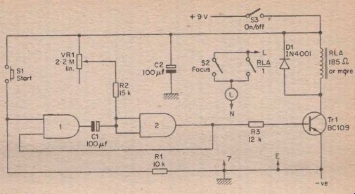
FIG. 22 Enlarger timer (use only I.C.4001) of the enlarger.
C1 must be a high quality component having a low leakage current if reliable and consistent results are to be obtained.
It is necessary to mark a dial around the control knob of VR1, and this should preferably be calibrated at one second Intervals. Marking this out is rather time consuming since the only way to find the calibration points is to use trial and error.
Peak Level Indicator
A peak level indicator is a device which will give a warning of an over load in an amplifier, tape recorder, mixer, or some other piece of audio gear. Unlike the usual average reading VU meter, this type of indicator has a very fast response and it will respond to even very brief transients as it is operated by peak rather than average or R.M.S. levels.
It must be emphasized that a peak level indicator is not intended to be used instead of a VU meter, but is intended to be used in conjunction with one. A single peak level indicator will only show when an over load has occurred. It does not show, the signal level.
The circuit diagram of a peak level indicator which utilizes a CMOS monostable is shown in Figure 23. Gates 2 and 3 form the monostable, and the output of this is used to drive L.E.D. indicator Dl via current limiting resistor R6. The L.E.D. indicator will come on when the output of the monostable goes positive. The circuit values have been chosen to produce an output pulse of about 0.2 seconds in duration.
R3 and R4 are used to bias the input of the monostable towards its trigger voltage, but the voltage produced by this potential divider is insufficient to actually trigger the circuit. The reason for using this network is that it reduces the peak input voltage which is required in order to trigger the monostable, and it thus increases the sensitivity of the circuit.
It does not increase the sensitivity quite enough to enable the unit to be used with some pieces of equipment, and so an amplifier stage has been included ahead of the monostable. This is based on gate...I, and the use of the CMOS gates as linear amplifiers will be covered more fully later. R1 is a sensitivity control, and this enables the unit to be adjusted to respond to any input signal level of about 500 mV peak to-peak or more.
The amplified input signal will modulate the voltage at the input of the monostable, and when a positive peak takes the input above the transfer voltage of the gate the monostable will be triggered. This will cause D1 to be briefly pulsed on.
of the enlarger.
C1 must be a high quality component having a low leakage current if reliable and consistent results are to be obtained.
It is necessary to mark a dial around the control knob of VR1, and this should preferably be calibrated at one second Intervals. Marking this out is rather time consuming since the only way to find the calibration points is to use trial and error.
Peak Level Indicator
A peak level indicator is a device which will give a warning of an overload in an amplifier, tape recorder, mixer, or some other piece of audio gear. Unlike the usual average reading VU meter, this type of indicator has a very fast response and it will respond to even very brief transients as it is operated by peak rather than average or R.M.S. levels.
It must be emphasized that a peak level indicator is not intended to be used instead of a VU meter, but is intended to be used in conjunction with one. A single peak level indicator will only show when an overload has occurred. It does not show the signal level.
The circuit diagram of a peak level indicator which utilizes a CMOS monostable is shown in Figure 23. Gates 2 and 3 form the monostable, and the output of this is used to drive L.E.D. indicator D1 via current limiting resistor R6. The L.E.D. indicator will come on when the output of the monostable goes positive. The circuit values have been chosen to produce an output pulse of about 0.2 seconds in duration.
R3 and R4 are used to bias the input of the monostable towards its trigger voltage, but the voltage produced by this potential divider is insufficient to actually trigger the circuit. The reason for using this network is that it reduces the peak input voltage which is required in order to trigger the monostable, and it thus increases the sensitivity of the circuit.
It does not increase the sensitivity quite enough to enable the unit to be used with some pieces of equipment, and so an amplifier stage has been included ahead of the monostable. This is based on gate. 1, and the use of the CMOS gates as linear amplifiers will be covered more fully later. R1 is a sensitivity control, and this enables the unit to be adjusted to respond to any input signal level of about 500 mV peak to peak or more.
The amplified input signal will modulate the voltage at the input of the monostable, and when a positive peak takes the input above the transfer voltage of the gate the monostable will be triggered. This will cause D1 to be briefly pulsed on.
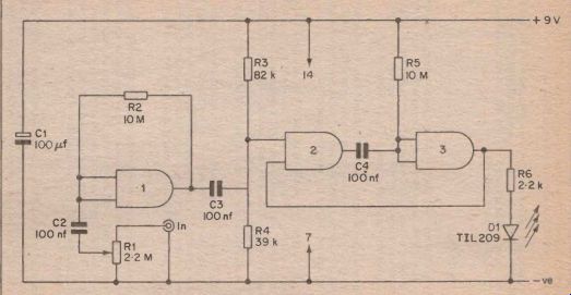
FIG. 23 Peak level indicator circuit (only use I.C. 4001).
It is an essential feature of the circuit that it is the peak level of the signal which the circuit responds to, the input waveshape and its mean level being irrelevant. In order to obtain consistent operation from this circuit it is necessary to power it from a stabilized supply.
An input for the unit is taken from any suitable point in the VU meter circuit, and as the unit has an input impedance of around 2 Megohms it will not significantly load the VU meter circuit. Because of this very high input impedance it may be beneficial to use screened input cable, although this will not be necessary if the unit is fed from a fairly low source impedance.
R1 is adjusted in the following manner. Connect a sinewave generator to the input of the main equipment and adjust the controls to indicate the required overload level on the VU meter (usually either +3 or +6 dB). Adjust R1 for the lowest sensitivity which causes the L.E.D. indicator to be continuously on.
Stereo Version
For stereo operation it is possible to use two of these peak level indicators, one to monitor each channel. It is more convenient however, to use a circuit which uses one indicator lamp for both channels. This can be accomplished by feeding the outputs of two of the circuits described above to the circuit shown in Figure 24. R6 and D1 of each of the original circuits are omitted, and the present circuit is fed direct from the outputs of the monostables.
FIG. 24 When used in conjunction with two modified versions of Fig. 23 this
produces a stereo P.L.I. (use only I.C. 4001).
It is an essential feature of the circuit that it is the peak level of the signal which the circuit responds to, the input waveshape and its mean level being irrelevant. In order to obtain consistent operation from this circuit it is necessary to power it from a stabilized supply.
An input for the unit is taken from any suitable point in the VU meter circuit, and as the unit has an input impedance of around 2 Megohms it will not significantly load the VU meter circuit. Because of this very high input impedance it may be beneficial to use screened input cable, although this will not be necessary if the unit is fed from a fairly low source impedance.
R1 is adjusted in the following manner. Connect a sinewave generator to the input of the main equipment and adjust the controls to indicate the required overload level on the VU meter (usually either +3 or +6 dB). Adjust R1 for the lowest sensitivity which causes the L.E.D. indicator to be continuously on.