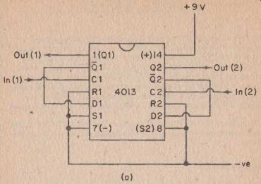
FIG. 43(a) A 4013 I.C. can be used to form two divide by two circuits
| Home | Audio mag. | Stereo Review mag. | High Fidelity mag. | AE/AA mag. |
The previous Sections have been concerned with circuits based on simple inverters and gates, with all the projects being based on the 4001 and 4011 I.C.s. These are only two devices from a vast range of CMOS devices which are now available. It must be admitted that many of the I.C.s in this range are for highly specialized applications, and are of little use to the amateur enthusiast. On the other hand, there are several devices which can be usefully employed by the amateur, the frequency divider I.C.S being the most obvious examples.
In this SECTION, details of some of the more specialized CMOS I.C.s will be given, together with some practical details of their use in simple projects.
Frequency Dividers
These are almost certainly the most useful of the specialized CMOS devices, and four types will be considered here. These are the 4013 type D flip flop, the 4027 J -K master slave flip flop, the 4017 decade counter, and the 4018 pre-settable divide by 'N' counter. The latter can be connected so that it will divide by any even number from two to ten (inclusive), and it will be discussed separately from the other three devices.
The most simple of the CMOS frequency dividers is the 4013, and this contains two D type flip flops. In order to get this type of circuit to divide by two it is merely necessary to connect the Q output to the data input, and earth the set and reset terminals. The input is then applied to the clock terminal and the output is obtained from the Q output.
Connection details for the 4013 are shown in Figure 43(a). If only a single divide by two circuit is required, the clock input of the unused device should be connected to the negative supply rail. It is possible to obtain a divide by four action by connecting the output of one flip flop to the output of the other one.
The 4027 I.C. contains two J-K flip flops, and the circuit diagram of Figure 43(b) shows how these are connected to provide a divide by two action. Again it is possible to obtain a divide by four action by using the two flip flops in series.
Connection details for the 4017 decade counter, or divide by ten circuit, is shown in Figure 43(c). This is very simple with the input being applied to the clock terminal and the output being obtained from the carry out terminal. The reset and clock enable terminals must be earthed.
FIG. 43(a) A 4013 I.C. can be used to form two divide by two circuits
An interesting feature of this device is that it has ten outputs apart from the carry out one. These are marked '0' to '9' in Figure 43(c).
These go high for one complete clock cycle in sequence. Thus during the first clock input cycle the '0' output goes high, then the '1' output goes high for the next cycle, and so on until the '9' output has gone , high for one cycle. Then the whole sequence starts again from the beginning. This feature can be used to operate the 4017 as a preset-table divide by N counter, but additional active circuit elements are required, and in most instances it is easier and cheaper to use the 4018 I.C. However, there are other applications in which this series of output pulses can be utilized.
---
Crystal Calibrators
Probably the most obvious use for a frequency divider is in a crystal calibration oscillator, and a simple circuit using a 4017 in this role is shown in Figure 44.
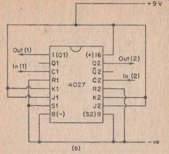
FIG. 43(b) A 4027 I.C. can be used to provide the same function.
Here a couple of inverters are used in a simple crystal oscillator of the type shown earlier in Figure 27. This operates at a frequency of 1 MHz and has its output fed to the clock input of the 4017. An output frequency of 100 kHz therefore appears at the output of the 4017, and this circuit thus provides outputs at both 1 MHz and 100 kHz.
This could, of course, be achieved using two separate oscillators, one at each frequency, or by using two switched crystals. This method is preferable though, since crystals are far more expensive than the 4017 I.C.
The outputs of this circuit have fast rise and fall times, and the outputs are therefore rich in the required harmonics. It provides marker frequencies at 1 MHz intervals from 1 MHz to over 30 MHz, and at 100 kHz intervals from 100 kHz to over 30 MHz. The unit is thus suitable for calibrating general coverage M.W./S.W. receivers.
For optimum accuracy to be obtained it is necessary to trim the oscillator frequency to precisely 1 MHz. Probably the easiest way to do this is to connect a lead to the 100 kHz output of the unit, and place this near to an operating receiver which is tuned to Radio 2 on the L.W. band. B.B.C. Radio 2 operates at precisely 200 kHz on the L.W. band, and the first harmonic of the 1CV0 kHz signal will react with the Radio 2 signal to produce a beat note. This note will be very low in pitch, and C2 is adjusted to produce the lowest possible beat note. With careful tuning of the oscillator it should be possible to obtain a beat note of less than 1 Hz.
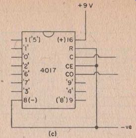
FIG. 43(c) A 4017 I.C. connected as a divide by 10 circuit
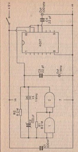
FIG. 44 A simple 1 Mhz 1100 kHz crystal calibration oscillator.
For most purposes such a high degree of accuracy is not required, and it is usually possible to obtain more than adequate accuracy by leaving out the trimmer capacitor (C2), and connecting the crystal in parallel with R2.
It is worth noting that most receivers have spurious responses and misleading results can be obtained if the calibration signal is picked up on one of these. For this reason it is advisable to use only a very loose coupling between the receiver and the calibrator, and it will probably not be necessary to use a direct coupling at all. Simply placing a lead connected to the appropriate output of the calibrator close to the receiver's aerial socket should suffice.
Triple Output Version
The crystal calibration of Figure 44 is excellent for calibrating general coverage receivers, but it leaves a lot to be desired when it comes to the calibration of an amateur bands only set. For instance, the 80 Meter band extends from 3.5 to 3.8 MHz, and so the calibrator would only provide calibration points at the band limits, plus two inside these limits.
For this reason it is quite common for calibrators intended for use with amateur bands receivers to have a very low output frequency in addition FIG. 4 3(c) A 4017 I.C. connected as a divide by 10 circuit For most purposes such a high degree of accuracy is not required, and it is" usually possible to obtain more than adequate accuracy by leaving out the trimmer capacitor (C2), and connecting the crystal in parallel with R2.
For this reason it is quite common for calibrators intended for use with amateur bands receivers to have a very low output frequency in addition to the normal ones. This can easily be achieved with the circuit of Figure 44 by simply adding an extra decade counter at the 100 kHz output. This then provides outputs at 1 MHz, 100 kHz, and 10 kHz.
The modified circuit is shown in Figure 45.
This is set up and used in the same way as the original circuit.
Simple Calibration Oscillator
Although L-C oscillators do not provide such good accuracy and stability as crystal ones, it is nevertheless possible to make a perfectly satisfactory calibration oscillator using an L-C oscillator. The circuit diagram of such a device is shown in Figure 46.
Inverter 1 is used as an inductive feedback oscillator of the type used in the B.F.O./I.F. Alignment oscillator of Figure 29. In this case the tuned circuit is a Denco M.W. R.F. transformer, and the frequency of oscillation is tunable over the H.F. end of the M.W. band (about 1.7 to 0.8 MHz) by means of VC1. In practice the oscillator is tuned to a frequency of 1 MHz.
Inverter 2 is used as a sort of buffer amplifier, and the amplitude of the signal at its output is sufficient to properly drive the clock input of the 4017 decade counter. A 100 kHz output signal is, of course, obtained from the output of the 4017. The unit therefore provides calibration signals at 1 MHz, 100 kHz, and their harmonics.
The circuit is set up and used in much the same way as the crystal calibrators, but it must be remembered that the crystal oscillators have only a very restricted tuning range, whereas this circuit covers a fairly wide range of frequencies. VC1 will almost certainly need some adjustment before a beat note can be obtained. When a beat note has been obtained; VC1 is adjusted for zero beat in the same way as for a crystal oscillator, but it is unlikely that the unit can be adjusted as precisely as a crystal oscillator. The long term stability of this unit will not be as good as that of a crystal controlled unit, and it is advisable to set the unit up against Radio 2 whenever it is used.
It is not a good idea to solder direct to the pins of T1 as this has a polystyrene former which will melt with the heat of the soldering iron. The pins at the base of the coil will fit a B9A valveholder, and it is strongly recommended that the coil is mounted in one of these, and that the soldered connections are made to the holder. The core of the coil is screwed right down when the coil is received, and it must be unscrewed slightly so that about 10 mm of metal screw-thread protrudes from the top of the coil.
The pin numbers shown in Figure 46 show the correct phasing for the coil, and it is essential that this is correct. There are actually three windings on the coil, but the one connected across pins 8 and 9 ignored. The full description of the coil (which must be given when ordering it) is 'Yellow R.F. coil for transistor usage, Range 2T'.
The modified circuit is shown in Figure 45.
This is set up and used in the same way as the original circuit.
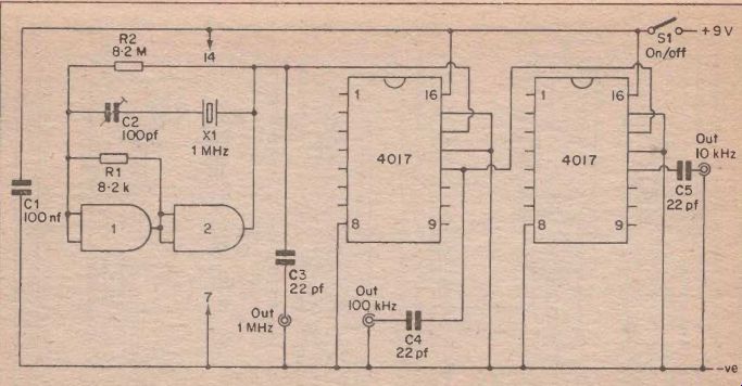
FIG. 45 A 1MHz/100 kHz/10 kHz crystal calibrator
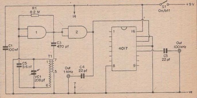
FIG. 46 An inexpensive 1MHz/100 kHz calibration oscillator
All the calibrator circuits shown here have used the 4017 I.C., but the oscillators could just as easily be used to feed a 4013 or 4027 device.
In this case the two halves of these I.C.s would be connected in series, and fundamental output frequencies of 1 MHz, 500 kHz, and 250 kHz would be obtained. It would not be possible to set these circuits up against Radio 2 on the L.W. band since there would be no output at 200 kHz, but the standard frequency transmission at 5 MHz could be used instead.
The circuit of Figure 45 is not restricted to use as a crystal oscillator, and circuits of this type are found in many digital electronic circuits.
Frequency meters and electronic timers are typical examples. In such applications it will probably be necessary to add extra division stages, but this is very easily accomplished.
Risetime
One point that must be borne in mind when using CMOS frequency dividers is that for reliable operation they require an input signal having a fast risetime. The input waveform should have a risetime of less than 5 micro -seconds and should be more than 0.5 micro seconds wide.
If a CMOS divider is to be used successfully use from a slow input wave form it must have some form of speed-up circuit added at the input.
One way of achieving this is to add a Schmitt trigger at the input, as shown in Figure 47. The way in which the Schmitt trigger works will not be considered here as it was fully dealt with in the previous SECTION.
The way in which it speeds up the input waveform is simple. As the input waveform rises it will have no effect on the output of the Schmitt trigger until it reaches the threshold voltage of the trigger. Then the output very rapidly swings positive and operates the divider. It is on the positive edge of the waveform that the divider is operated.
Electronic Game
It was mentioned earlier that the 4017 I.C. has ten outputs apart from the usual carry out one. Five of these outputs are utilized in the circuit of Figure 48 which shows how the device can be used as the basis of a simple electronic game. It also demonstrates the properties of the 4017 I.C.
The two inverters are used in an astable multivibrator, and the operating frequency of this can be varied from less than 1 Hz to over 100 Hz by means of VR1. The output of the multivibrator is used to drive the clock input of the 4017.
ignored. The full description of the coil (which must be given when ordering it) is 'Yellow R.F. coil for transistor usage, Range 2T. All the calibrator circuits shown here have used the 4017 I.C., but the oscillators could just as easily be used to feed a 4013 or 4027 device.
In this case the two halves of these I.C J would be connected in series, and fundamental output frequencies of 1 MHz, 500 kHz, and 250 kHz would be obtained. It would not be possible to set these circuits up against Radio 2 on the L.W. band since there would be no output at 200 kHz, but the standard frequency transmission at 5 MHz could be used instead.
The circuit of Figure 45 is not restricted to use as a crystal oscillator, and circuits of this type are found in many digital electronic circuits.
Frequency meters and electronic timers are typical examples. In such applications it will probably be necessary to add extra division stages, but this is very easily accomplished.
Rise time
One point that must be borne in mind when using CMOS frequency dividers is that for reliable operation they require an input signal having a fast risetime. The input waveform should have a risetime of less than 5 micro-seconds and should be more than 0.5 microseconds wide.
If a CMOS divider is to be used successfully use from a slow input waveform it must have some form of speed-up circuit added at the input.
One way of achieving this is to add a Schmitt trigger at the input, as shown in Figure 47. The way in which the Schmitt trigger works will not be considered here as it was fully dealt with in the previous SECTION.
The way in which it speeds up the input waveform is simple. As the input waveform rises it will have no effect on the output of the Schmitt trigger until it reaches the threshold voltage of the trigger. Then the output very rapidly swings positive and operates the divider. It is on the positive edge of the waveform that the divider is operated.
Electronic Game
It was mentioned earlier that the 4017 I.C. has ten outputs apart from the usual carry out one. Five of these outputs are utilized in the circuit of Figure 48 which shows how the device can be used as the basis of a simple electronic game. It also demonstrates the properties of the 4017 I.C.
The two inverters are used in an astable multivibrator, and the operating frequency of this can be varied from less than 1 Hz to over 100 Hz by means of VR1. The output of the multivibrator is used to drive the clock input of the 4017.
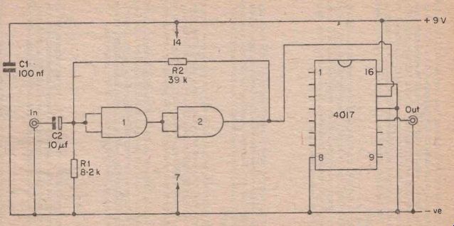
FIG. 47 A Schmitt trigger con be used to reliably operate a divider circuit
from a slowly rising wove form
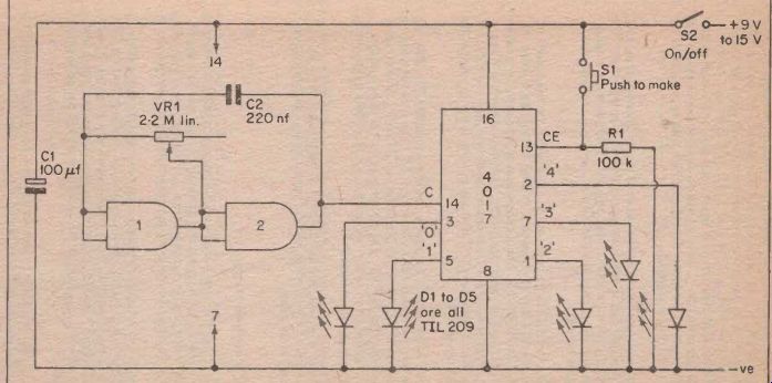
FIG. 48 Simple electronic game.
The clock enable terminal of the 4017 is connected to earth through R1, and so when S2 is closed and power is applied to the circuit, the 4017 will start to operate. The first input cycle will cause pin 3 (the '0' output) to go high, and the first L.E.D. will light up. At the commencement of the next clock input cycle pin 3 will return to the low state and pin 5 (the '1' output) will go high for one complete input cycle. Then pin 5 goes low and pin 1 goes high, and so on until all the L.E.D.s have turned on in sequence.
There is then a pause during which none of the L.E.D.s come on, and this is the period during which the unconnected outputs go high. When all five of these outputs have gone high the cycle starts once again from the beginning, with the five L.E.D.s turning on in sequence followed by a break.
In practice the L.E.D.s are mounted in a row along the front panel of the unit, and the idea of the game is to stop the sequence when the middle L.E.D. (D3) is on. The sequence is stopped simply by pressing Si which is a push to make non -locking push button switch. When this is operated it takes the clock enable input high, and this blocks the clock signal and holds the 4017 in whatever state it was in when at the instant Si was closed.
The circuit is reset ready for a new round by releasing S1. The sequence then continues from where it left off. The speed at which the circuit operates, and therefore the degree of difficulty, is controlled by the setting given to VR1. The circuit may appear to be one that tests the reaction speed of the competitor, but it is really more a test of co-ordination and anticipation.
It is possible to use the circuit from a 9 volt supply, but the L.E.D. display will not be very bright and it is better to use a supply voltage of about 12 to 15 volts.
The 4018 Pre-settable Divider
Almost certainly the most versatile of the inexpensive CMOS frequency divider I.C.s is the 4018 pre-settable divide by N counter. This can be used to divide by any even number from 2 to 10 inclusive. Figure 49 shows the necessary connections to obtain a divide by ten action.
The basic way in which the device operates is quite simple to under stand. The clock signal is divided by 2 at the Q1 output, 4 at the Q2 output, 6 at the Q3 output, 8 at the Q4 output, and 10 at the Q5 output. In Figure 49 the Q5 output is coupled to the data input, and therefore after ten input cycles the circuit is reset and the pulse count starts again.
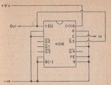
FIG. 49 The 4018 as a decode counter
In order to obtain a divide by two action the Q1 output is connected to the data input instead of having the Q5 input coupled to it. Connect the data input to Q2 for a divide by 4 action, to Q3 for a divide by six action, or to Q4 for a divide by 8 action.
In common with the other CMOS frequency dividers considered here, the 4018 will operate satisfactorily up to input frequencies of about 5 MHz when it is used with a 9 V supply line.
Display Driver
One of the most useful and interesting of the I.C.s in the CMOS range is the 4026 which is a decade counter and decoder. Conventionally a separate decade counter and decoder I.C. are used to provide a digital readout, but the 4026 performs both these functions and this consider ably reduces the complexity of digital systems in which it is used.
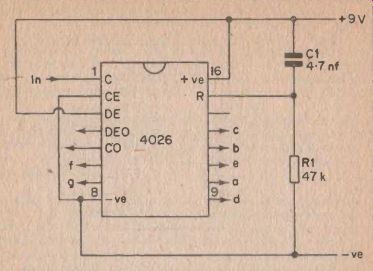
FIG. 50 The 4026 decode counter/readout I.C.
Another advantage of this I.C. over most others is that it does not need to drive the output display via either switching transistors or current limiting resistors. It can be used to drive a low current seven segment display direct. The author has used this device successfully with a DL704E seven segment L.E.D. indicator, but it should work just as well with any similar device.
The circuit diagram shown in Figure 50 shows how the 4026 can be connected to operate as a simple pulse counter. The display will show the number of output pulses received at the clock input up to a maximum of nine, after which the display goes back to zero and starts counting up to nine again. In virtually all practical applications a maximum count of more than nine will be required, and the circuit can be made to count as high as one wishes simply by connecting the carry out terminal of this circuit to the clock input of a second identical circuit. The carry out input divides the clock input by ten, and so the first circuit counts the units (and drives the left hand display) while the second one counts the tens (and drives the right hand digit).
Obviously, by adding further digits the circuit can be made to count thousands, tens of thousands, and so on. Note that the 4026 can only be used to directly drive common cathode displays, and is not suitable for direct interface with common anode ones (such as the DL707E).
Apart from the useful features already mentioned, the 4026 has a few others. Pin 2 is a clock enable input, and the circuit operates normally when this is low, and fails to respond to input pulses when it is high.
In many applications the clock signal is fed to the counter circuit via an enabling gate. When the 4026 is used in such applications a separate control gate is not necessary, and this input can be fed with the control signal instead.
When pin 3 is high the circuit works normally, but when it is low the display is switched off. The I.C. is operative in all other respects. This is very useful since it means that the display is easily controlled, and the number of output pulses received at the clock input up to a maximum of nine, after which the display goes back to zero and starts counting up to nine again. In virtually all practical applications a maximum count of more than nine will be required, and the circuit can be made to count as high as one wishes simply by connecting the carry out terminal of this circuit to the clock input of a second identical circuit. The carry out input divides the clock input by ten, and so the first circuit counts the units (and drives the left hand display) while the second one counts the tens (and drives the right hand digit).
Obviously, by adding further digits the circuit can be made to count thousands, tens of thousands, and so on. Note that the 4026 can only be used to directly drive common cathode displays, and is not suitable for direct interface with common anode ones (such as the DL707E).
Apart from the useful features already mentioned, the 4026 has a few others. Pin 2 is a clock enable input, and the circuit operates normally when this is low, and fails to respond to input pulses when it is high.
In many applications the clock signal is fed to the counter circuit via an enabling gate. When the 4026 is used in such applications a separate control gate is not necessary, and this input can be fed with the control signal instead.
When pin 3 is high the circuit works normally, but when it is low the display is switched off. The I.C. is operative in all other respects. This is very useful since it means that the display is easily controlled, and need only be switched on when a reading is to be taken. Economic battery operation is therefore possible where it might otherwise not be.
A display enable output is provided at pin 4, and this can be used to drive the decimal point of a display.
The reset input is usually connected to the negative supply via a resistor, and the counter can be reset to zero by a brief positive pulse to this input. In Figure 50 R1 ties the reset to earth and C1 provides a brief positive pulse at switch on which ensures that the counter starts at zero. If a push button switch is connected in place of C1 it is possible to reset the circuit manually.
There are many applications for which the 4026 is ideally suited, but most of these are too complicated to come within the scope of this book. One simple novelty application is as an electronic random number indicator unit, and a simple circuit for one of these is shown in Figure 51.
The two inverters operate as a 1 kHz astable multivibrator and are used to feed the clock input of I.C.1. The carry out terminal of I.C.1 is in turn used to feed the clock input of I.C.2. These two I.C.s plus the two readout devices thus form a two digit counter.
As the circuit stands, the display will be off and the clock signal will be muted. If S2 is pressed, the clock signal will operate the counter, and it will take the counter through a complete 00 to 99 count about ten times per second. When S2 is released, the counter will stop at what ever number it happened to be at the instant S2 broke the clock enable circuit to earth.
What this number happens to be is quite unpredictable, and in this way the circuit operates as a random number indicator. The unit can be made to display the number by operating S1 which connects the display enable terminals to the positive supply.
S3 is the normal on/off switch.
Bilateral Switches
A bilateral switch is a type of enabling gate, except whereas most enabling gates are only suitable for use with pulsed signals, a bilateral switch can be used in linear applications. For low signal levels the typical distortion level through a bilateral switch is only about 0.4%.
There are two readily available CMOS bilateral switches, the 4016 and the 4066. These are both contained in a 14 pin DIL package and have the pinning arrangement shown in Figure 52. The main difference between these two devices is that the 4016 will operate at frequencies up to about 10 MHz while the 4066 will work up to 40 MHz.
need only be switched on when a reading is to be taken. Economic battery operation is therefore possible where it might otherwise not be.
A display enable output is provided at pin 4, and this can be used to drive the decimal point of a display.
The reset input is usually connected to the negative supply via a resistor, and the counter can be reset to zero by a brief positive pulse to this input. In Figure 50 R1 ties the reset to earth and C1 provides a brief positive pulse at switch on which ensures that the counter starts at zero. If a push button switch is connected in place of C1 it is possible to reset the circuit manually.
There are many applications for which the 4026 is ideally suited, but most of these are too complicated to come within the scope of this book. One simple novelty application is as an electronic random number indicator unit, and a simple circuit for one of these is shown in Figure 51.
The two inverters operate as a 1 kHz astable multivibrator and are used to feed the clock input of I .C . 1 . The carry out terminal of I.C.1 is in turn used to feed the clock input of I.C.2. These two I.C.s plus the two readout devices thus form a two digit counter.
As the circuit stands, the display will be off and the clock signal will be muted. If S2 is pressed, the clock signal will operate the counter, and it will take the counter through a complete 00 to 99 count about ten times per second. When S2 is released, the counter will stop at whatever number it happened to be at the instant S2 broke the clock enable circuit to earth.
What this number happens to be is quite unpredictable, and in this way the circuit operates as a random number indicator. The unit can be made to display the number by operating S1 which connects the display enable terminals to the positive supply.
S3 is the normal on/off switch.
Bilateral Switches
A bilateral switch is a type of enabling gate, except whereas most enabling gates are only suitable for use with pulsed signals, a bilateral switch can be used in linear applications. For low signal levels the typical distortion level through a bilateral switch is only about 0.4%.
There are two readily available CMOS bilateral switches, the 4016 and the 4066. These are both contained in a 14 pin DIL package and have the pinning arrangement shown in Figure 52. The main difference between these two devices is that the 4016 will operate at frequencies up to about 10 MHz while the 4066 will work up to 40 MHz.
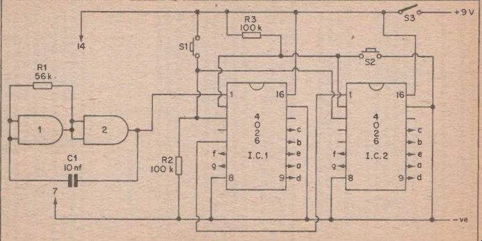
FIG. 51 The circuit diagram of a simple electronic random number indicator
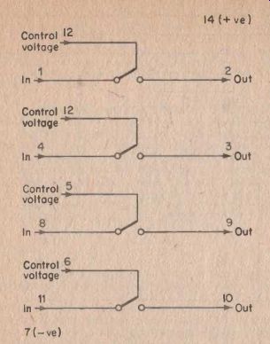
FIG. 52 The leadout diagram for the 4016 and 4066 I.C.s
The on resistance of the switches is approximately 300 ohms and the off resistance is about 1 million Megohms. The switches are off when the control voltage is low and on when it is high. Signal levels of about two volts peak to peak can be handled when these devices are operated from a single supply rail, but when operated from a dual balanced supply they can handle peak to peak signal voltages equal to the sum of the supply rail voltages.
As will be apparent from Figure 52, the 4016 and 4066 devices each contain four bilateral switches, and this makes these devices very versatile.
It is worth noting that although each switch has an input and output legend in Figure 52, this has only been done as it is more convenient to think in these terms when considering practical uses for these devices, than just simply using pin numbers for identification purposes.
These switches are, as their name states, bilateral, and in practice it would seem to be possible to use them either way round.
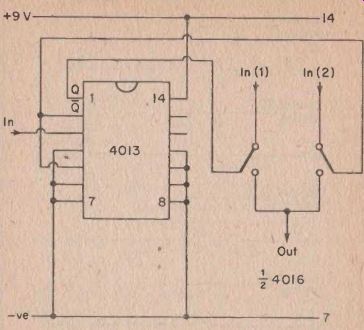
FIG. 53 A simple electronic switch
These switches are only single throw types, but it is possible to obtain a double throw action by using two switches with the outputs connected in parallel. The control terminals of the switches must be fed from a circuit which ensures that they are always in antiphase, with one switch in the on state and the other in the off condition.
This can be achieved by feeding the switches from the Q and Q outputs of a flip flop circuit, such as the 4013 type D flip flop. Such a circuit is shown in Figure 53.
The 4013 is connected as a divide by two circuit with one of the two flip flops it contains being unused. The two outputs of the 4013 are always in the opposite logic state and these states change with each successive input pulse. If, for instance, the Q output is high and the Q one is, low when the power supply is initially connected to the circuit, then input 1 will be enabled and input 2 will be blocked.
Applying a brief input pulse to the circuit will cause the flip flop to change state, and then input 1 will be blocked and input 2 will be enabled. The circuit thus provides a purely electronic S.P.D.T. switch.
These switches are only single throw types, but it is possible to obtain a double throw action by using two switches with the outputs connected in parallel. The control terminals of the switches must be fed from a circuit which ensures that they are always in antiphase, with one switch in the on state and the other in the off condition.
This can be achieved by feeding the switches from the Q and Q outputs of a flip flop circuit, such as the 4013 type D Hip flop. Such a circuit is shown in Figure 53.
The 4013 is connected as a divide by two circuit with one of the two flip flops it contains being unused. The two outputs of the 4013 are always in the opposite logic state and these states change with each successive input pulse. If, for instance, the Q output is high and the Q one is low when the power supply is initially connected to the circuit, then input 1 will be enabled and input 2 will be blocked.
Applying a brief input pulse to the circuit will cause the Hip flop to change state, and then input 1 will be blocked and input 2 will be enabled. The circuit thus provides a purely electronic S.P.D.T. switch.
Several variations on this basic circuit are possible. By paralleling the inputs instead of the outputs, the circuit will then channel the single input circuit to only one of two circuits connected at the output. By simply omitting one of the bilateral switches a purely electronic S.P.S.T. switch is produced. By connecting two further bilateral switches in the same configuration as the original two, and feeding one control input from each output of the 4013, a D.P.D.T. action is obtained.
When contemplating using one of these switches always bear in mind the limitations on both the signal amplitude and impedance. For example, the D.P.D.T. version of this switch could not be used as the send/receive switch of an intercom, as although it could probably be made to handle the signal amplitudes by use of a dual balanced supply, the 300 ohm series resistance of each switch would limit the output to the speakers to an unsatisfactory level. The 4016 device is specified in the circuits described here since there are very few applications where the additional performance of the 4066 is required, and the 4016 is less expensive and more widely available.
Touch Switch
In simple applications a touch activated version of the circuit of Figure 53 is probably of more use. Such a circuit appears in Figure 54.
Here two inverters are used as a bistable multivibrator with high value cross coupling resistors. This makes the circuit sufficiently sensitive to be operated by touch contacts. We will assume for the sake of this circuit explanation that the circuit takes up the state of having inverter 1 output low and inverter 2 output high when the supply is initially connected (although it could in fact taken up the opposite state).
In order to trigger the circuit into the opposite state, and so reverse the states of the bilateral switches, it is merely necessary to touch the left hand set of touch contacts. This takes the input of inverter 1 low since it will be connected to earth through the skin resistance of the operator. This sends the output of inverter 1 high which in turn takes the input of inverter 2 high due to the coupling by way of R2. Inverter 2 output therefore goes low, and inverter 1 input will therefore stay in the low state even when the operator's finger is removed from the touch contacts, since it will be held low by being coupled to the low output of inverter 2 by way of R1.
The circuit can be reset to the original state by touching the right hand set of touch contacts. An identical circuit action then takes place, but the roles of the inverters are reversed this time.
It is possible to trigger the circuit from one state to the other indefinitely by operating each set of contacts in turn. There are, of course, no moving parts whatever to wear out Several variations on this basic circuit are possible. By paralleling the inputs instead of the outputs, the circuit will then channel the single input circuit to only one of two circuits connected at the output. By simply omitting one of the bilateral switches a purely electronic S.P.S.T. switch is produced. By connecting two further bilateral switches in the same configuration as the original two, and feeding one control input from each output of the 4013, a D.P.D.T. action is obtained.
When contemplating using one of these switches always bear in mind the limitations on both the signal amplitude and impedance. For example, the D.P.D.T. version of this switch could not be used as the send/receive switch off an intercom, as although it could probably be made to handle the signal amplitudes by use of a dual balanced supply, the 300 ohm series resistance of each switch would limit the output to the speakers to an unsatisfactory level. The 4016 device is specified in the circuits described here since there are very few applications where the additional performance of the 4066 is required, and the 4016 is less expensive and more widely available.
Touch Switch
In simple applications a touch activated version of the circuit of Figure 53 is probably of more use. Such a circuit appears in Figure 54.
Here two inverters are used as a bistable multivibrator with high value cross coupling resistors. This makes the circuit sufficiently sensitive to be operated by touch contacts. We will assume for the sake of this circuit explanation that the circuit takes up the state of having inverter 1 output low and inverter 2 output high when the supply is initially connected (although it could in fact taken up the opposite state).
In order to trigger the circuit into the opposite state, and so reverse the states of the bilateral switches, it is merely necessary to touch the left hand set of touch contacts. This takes the input of inverter 1 low since it will be connected to earth through the skin resistance of the operator. This sends the output of inverter 1 high which in turn takes the input of inverter 2 high due to the coupling by way of R2. Inverter 2 output therefore goes low, and inverter 1 input will therefore stay in the low state even when the operator's finger is removed from the touch contacts, since it will be held low by being coupled to the low output of inverter 2 by way of R1.
The circuit can be reset to the original state by touching the right hand set of touch contacts. An identical circuit action then takes place, but the roles of the inverters are reversed this time.
It is possible to trigger the circuit from one state to the other indefinitely by operating each set of contacts in turn. There are, of course, no moving parts whatever to wear out.
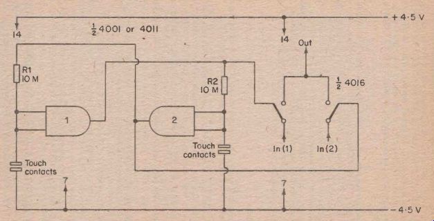
FIG. 54 An S.P. D.T electronic touch switch
As was the case with the circuit of Figure 53, several variations on this basic circuit are possible.
---------
Audio Squelch
Squelch circuits are commonly employed in F.M. tuners and receivers, and in V.H.F. communications equipment. With this type of equipment there is a high level of background noise in the absence of a signal, and the purpose of the squelch circuit is to mute the receiver unless a signal is present. This eliminates the very loud and hence annoying background hiss that occurs when tuning an F.M. set between stations, or when no signal is present at the input of a V.H.F. communications set.
In the case of this type of equipment the squelch circuit is usually activated by the carrier wave signal of the received transmission, rather than by the audio signal. There are however, audio applications where a squelch circuit can be useful. One example would be in the case of, a public address system which is being used in a noisy environment, with a fairly high background noise level being transmitted over the equipment.
In this case the squelch circuit would be adjusted so that it would not be activated by the normal background noise level (of human rather than an electrical origin), but so that it would only enable the equipment in the presence of a proper microphone signal.
There must be many other applications for such equipment apart from this one, and this is an application to which the 4016 is ideally suited.
The circuit diagram of an audio squelch unit using one of the bilateral switches in the 4016 I.C. is shown in Figure 55.
Operation of this circuit is quite straightforward. Some of the input signal is fed to the input of the bilateral switch and the remainder is fed to a high gain common emitter amplifier via a gain control (VR1) and a D.C. blocking capacitor (C2). Tr1 is the basis of the amplifier and this has collector load resistor R1 and base bias resistor R2.
The output of this amplifier is fed to a rectifier and smoothing network using C3, D1, D2, C4 and R3. The output of this network is fed to the control input of the bilateral switch.
VR1 is adjusted so that the control voltage fed to the bilateral switch is insufficient to enable the switch with only a background signal being fed to the input, but it is adjusted so that this voltage is only just short of the trigger voltage of the switch. Therefore, when a proper input signal is present, the trigger voltage will be exceeded and the switch will be enabled. The unit thus provides the required squelch action.
-----------------
Audio Squelch
Squelch circuits are commonly employed in F.M. tuners and receivers, and in V.H.F. communications equipment. With this type of equipment there is a high level of background noise in the absence of a signal, and the purpose of the squelch circuit is to mute the receiver unless a signal is present. This eliminates the very loud and hence annoying background hiss that occurs when tuning an F.M. set between stations, or when no signal is present at the input of a V.H.F. communications set.
In the case of this type of equipment the squelch circuit is usually activated by the carrier wave signal of the received transmission, rather than by the audio signal. There are however, audio applications where a squelch circuit can be useful. One example would be in the case of, a public address system which is being used in a noisy environment, with a fairly high background noise level being transmitted over the equipment.
In this case the squelch circuit would be adjusted so that it would not be activated by the normal background noise level (of human rather than an electrical origin), but so that it would only enable the equipment in the presence of a proper microphone signal.
There must be many other applications for such equipment apart from this one, and this is an application to which the 4016 is ideally suited.
The circuit diagram of an audio squelch unit using one of the bilateral switches in the 4016 I.C. is shown in Figure 55.
Operation of this circuit is quite straightforward. Some of the input signal is fed to the input of the bilateral switch and the remainder is fed to a high gain common emitter amplifier via a gain control (VR1) and a D.C. blocking capacitor (C2). Tr1 is the basis of the amplifier and this has collector load resistor R1 and base bias resistor R2.
The output of this amplifier is fed to a rectifier and smoothing network using C3, D1 , D2, C4 and R3. The output of this network is fed to the control input of the bilateral switch.
VR1 is adjusted so that the control voltage fed to the bilateral switch is insufficient to enable the switch with only a background signal being fed to the input, but it is adjusted so that this voltage is only just short of the trigger voltage of the switch. Therefore, when a proper input signal is present, the trigger voltage will be exceeded and the switch will be enabled. The unit thus provides the required squelch action.
As was the case with the circuit of Figure 53, several variations on this basic circuit are possible.
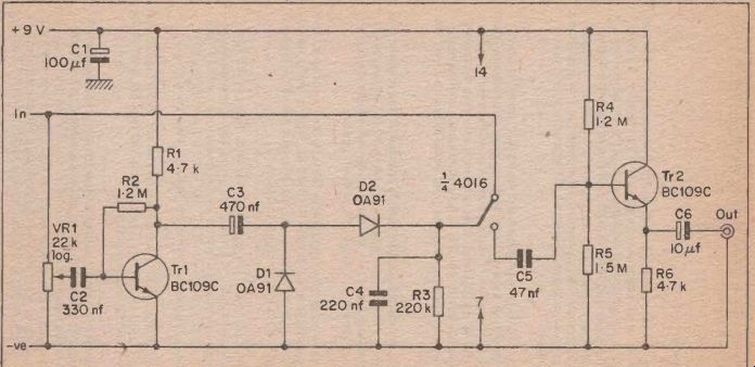
FIG. 55 An audio squelch unit
It is perhaps not entirely correct to call the voltage at which the bilateral switch changes state a trigger voltage, because this infers that the switch can only be fully on or fully off. This is not the case, and there is a range of control voltages over which it will be in an inter mediate state. Fortunately however, this range of voltages is very restricted, and the 4016 has a fairly well defined changeover voltage.
This circuit therefore works satisfactorily in practice without the need to incorporate any triggering.
The circuit has a fast attack and slow decay (hysteresis) which is necessary to ensure that the unit does not cut off during the brief pauses which occur during normal speech. The decay time can be altered to suit individual requirements by modifying the value of C4. The decay time is proportional to the value of this component, and it is something less than one second with the value shown in Figure 55.
Satisfactory operation of the device is possible with a nominal signal input level of less than 100 mV R.M.S. to a little more than 1 V_R.M.S. (sinewave input). The input impedance is about 10 k. Tr2 and associated components form an emitter follower output stage which provide the unit with a low output impedance.
C3 must be a high quality component if it is an electrolytic type, and it would probably be best to use a tantalum bead or plastic foil component here. Some electrolytic types have relatively high leakage currents which would result in the decay time of the circuit being greatly prolonged.
Automatic Cutout
This circuit is intended for use with disco and home movie equipment where the facility to automatically cut out a secondary channel (playing background music for instance) by applying a signal to the main input (such as a commentary) is required. The circuit diagram of this unit is shown in Figure 56.
The controlled input is fed to a gain control, and then to a bilateral switch. From here it is fed to the output via mixing resistor, R1.
Some of the main input is fed to gain control VR3, and then to mixing resistor R5. VR1 and VR3 allow the two input signals to be balanced to the required levels at the output. Some of the input signal at the main input is fed to a high gain common emitter amplifier by way of gain control (VR2) and D.C. blocking capacitor (C4).
The output from this amplifier is fed to a rectification and smoothing network using C2, D2, D1, C1 , and R2. The output of this network is fed to the control input of the bilateral switch.
It is perhaps not entirely correct to call the voltage at which the bilateral switch changes state a trigger voltage, because this infers that the switch can only be fully on or fully off. This is not the case, and there is a range of control voltages over which it will be in an intermediate state. Fortunately however, this range of voltages is very restricted, and the 4016 has a fairly well defined changeover voltage.
This circuit therefore works satisfactorily in practice without the need to incorporate any triggering.
The circuit has a fast attack and slow decay (hysteresis) which is necessary to ensure that the unit does not cut off during the brief pauses which occur during normal speech. The decay time can be altered to suit individual requirements by modifying the value of C4. The decay time is proportional to the value of this component, and it is something less than one second with the value shown in Figure 55.
Satisfactory operation of the device is possible with a nominal signal input level of less than 100 mV R.M.S. to a little more than 1 V_R.M.S. (sinewave input). The input impedance is about 10 k. Tr2 and associated components form an emitter follower output stage which provide the unit with a low output impedance.
C3 must be a high quality component if it is an electrolytic type, and it would probably be best to use a tantalum bead or plastic foil component here. Some electrolytic types have relatively high leakage currents which would result in the decay time of the circuit being greatly prolonged.
Automatic Cutout
This circuit is intended for use with disco and home movie equipment where the facility to automatically cut out a secondary channel (playing background music for instance) by applying a signal to the main input (such as a commentary) is required. The circuit diagram of this unit is shown in Figure 56.
The controlled input is fed to a gain control, and then to a bilateral switch. From here it is fed to the output via mixing resistor, R1 .
Some of the main input is fed to gain control VR3, and then to mixing resistor R5. VR1 and VR3 allow the two input signals to be balanced to the required levels at the output. Some of the input signal at the main input is fed to a high gain common emitter amplifier by way of gain control (VR2) and D.C. blocking capacitor (C4).
The output from this amplifier is fed to a rectification and smoothing network using C2, D2, D1, C1 , andR2. The output of this network is fed to the control input of the bilateral switch.
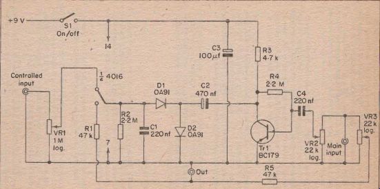
FIG. 56 An automatic cut out unit.
When no input signal is fed to the main input, the control input of the bilateral switch will be at earth potential, but as this is a positive earth circuit the control input is in fact high, and so the switch is enabled.
The controlled signal is therefore fed to the output.
If an input signal of sufficient level is applied to the main input, the negative D.C. bias produced across R2 and C1 will be virtually equal to the supply potential, and so the control input of the bilateral switch will be taken low, and the controlled input will be blocked. Thus the main input can be used to cut out the controlled one.
VR2 is given any setting which enables the main input to control the secondary one without spurious interruptions of the controlled input occurring. A minimum input amplitude of about 100 mV is required at the main input in order to cut off the secondary input.
As was the case with the previous circuit, the diode feed capacitor (C2) should be a high quality electrolytic type, or a plastic foil component.
Also in common with the previous circuit, this one has hysteresis, with the decay time of the circuit being variable by means of C1.
When no input signal is fed to the main input, the control input of the bilateral switch will be at earth potential, but as this is a positive earth circuit the control input is in fact high, and so the switch is enabled.
The controlled signal is therefore fed to the output.
If an input signal of sufficient level is applied to the main input, the negative D.C. bias produced across R2 and C1 will be virtually equal to the supply potential, and so the control input of the bilateral switch will be taken low, and the controlled input will be blocked. Thus the main input can be used to cut out the controlled on.
VR2 is given any setting which enables the main input to control the secondary one without spurious interruptions of the controlled input occurring. A minimum input amplitude of about 100 mV is required at the main input in order to cut off the secondary input.
As was the case with the previous circuit, the diode feed capacitor (C2) should be a high quality electrolytic type, or a plastic foil component.
Also in common with the previous circuit, this one has hysteresis, with the decay time of the circuit being variable by means of C1.