The Bask Op-amp R-C Oscillator
Like other active devices, op-amps can be used in the construction of oscillators. The simplest circuit has a "squarewave" output, uses only a few passive components in addition to the amplifier, and is very easy to design. Figure 3.1 shows two versions, for dual and single power supplies. The single-supply version has the advantage that for low frequencies the capacitor C1 can be an electrolytic type, though in most cases the capacitor of the split-supply version could be returned to the negative supply instead of ground.
The working of this oscillator is easier to follow from the dual-supply version of Figure 3.1a. In normal operation the output of the op-amp, Vow, is always as far as it can swing towards one of the supply rails. This places a voltage of R1/(R1+R2) x Vout on the non-inverting input whilst the capacitor C1 charges towards that voltage through R3. When it reaches it the output changes state, with a rapid switching action ensured by positive feedback through R2. The capacitor then starts charging in the opposite direction and this action repeats at a frequency deter mined by the resistors and capacitors used.
To simplify frequency calculations for this circuit a couple of assumptions can be made. The first is that if dual supplies are used, the positive and negative voltages are equal, or if a single supply is used the resistors R1a and R1 b are equal in value. In practice this will normally be the case. The second assumption is that the output of the op-amp can swing all the way to both supply rails. With a few exceptions this is not so, but it simplifies the calculation and provides an adequate starting point for practical experiments. The formula for frequency can then be calculated from:
p56
f - 1 2 x R1 ) x 1 R3 x C 1 2 x In (1 (2 x R1) + R2
This is a lot to punch into a calculator, even assuming that it has the exponential function "in" in its repertoire, so two much simpler versions are as follows. In many cases RI will be equal to R2, and the frequency is then given by:
0.455 f= R3 xC1
For the single-supply version, "R1" is the value of R1a and R1b in parallel. These will usually have the same value so it will be half the value of one of them. If equal value resistors are used for R1a, R1b and R2, "R1" will be half the value of R2 so the formula then becomes:
0.721 f = R3 x C 1
These two formulae provide a quick and simple estimate of the component values needed for most applications of this circuit. Its performance depends to a great extent on the band width of the op-amp used. Slow types can only be used at low frequencies and even here the slow rise and fall times of the output may be a disadvantage. The outputs of many op-amps can get closer to one supply voltage than the other, causing non symmetrical output, whilst the inability to swing all the way to one or both rails leads to deviation from the calculated frequency value. A few types may prove to be unstable in this circuit. The TL0xxx series of devices are stable and have outputs that, although not rail-to rail, have symmetrical offsets at either end. Most also have a good frequency response. A TL071 tested in the circuit of Figure 3.1b gave 1.0131cHz, and the variation with supply voltage from 5 to 25 volts was less than 1%. With a 1 n capacitor, for 10.6kHz, it gave 9.971cHz and with 100pF the output was 77kHz. The JFET inputs of this device also make it suitable for very low frequencies using high values of resistor R3.
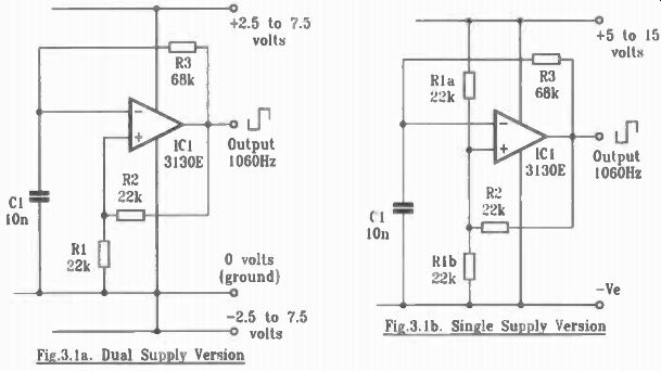
Fig. 3.1. Basic Op-amp Relaxation Oscillators.
Fig.3.1a. Dual Supply Version; Fig.3.1b. Single Supply Version
One of the best op-amps to use in this circuit is the 3130E. This is a CMOS device with very high input impedances and an output that, if lightly loaded, can swing all the way to both supply rails. In this application the usual frequency compensation is not needed, indeed it would merely slow the output switching. Since the 3130 is a CMOS device its supply voltage is limited to 15 volts or ±7.5 volts. With a 10 volt supply the test circuit delivered 1.024kHz and the variation with supply change between 7 and 15 volts was less than 0.2%. At 5 volts the output was still 1.016kHz. It also had a negligible tempera ture coefficient, though the passive components used with it did exhibit a small response to the freezer spray. This is far better than most CMOS logic gate oscillators and, for simple applications, it could be used as a reference frequency generator. At higher frequencies, changing the value of C1 to 1n produced 10kHz, and with 100pF the output was 86kHz.
The resistor R3 could be replaced by a diode and resistor net work for a non-symmetrical output, and for small frequency adjustments a variable resistor might be included. Varying this resistance gives a non-linear frequency response however, as it is the period of the output that is directly proportional to it. For a more linear adjustment range R2 can be made variable. A 220k resistor in series with R2 in Figure 3.1b, with a 1n capacitor for C1, resulted in a range of 10 kHz to 75 kHz with an almost linear control response. The variable resistor should be connected between the amplifier's output and R2, and the frequency rises as its value is increased. The supply current for this circuit is around 0.8mA, making this a good choice for a reference generator in battery operated designs.
Components for Figure 3.1b
Resistors (all metal film, 0.6W)
R1a, R1b, R2 22k (3 off)
R3 68k
Capacitors
C1 10n polyester or polystyrene
Semiconductors
IC1 3130 CMOS op-amp.
Triangle and Squarewave Oscillators
This is the equivalent of the integrator and comparator circuits shown in Figures 1.6 and 1.7. The performance is not usually quite as good because of the inability of most op-amp outputs to swing all the way to the supply rails, but it can be constructed using one of the many cheap dual op-amps available with very few additional passive components, so there will be occasions where it is useful.
Figure 3.2a shows a simple fixed frequency circuit. IC1 a is the integrator, whilst the comparator is IC1b with the level of hysteresis set by the ratio of resistors R2 and R3. When the output of the comparator is positive, current flowing into R1 causes IC1a's output to ramp towards negative at a rate set by R1 and C1. This output is connected to R2, the input to the comparator. When it is low enough, IC lb changes state and the change of polarity to R I starts the integrator output ramping in the opposite direction. Two outputs are available, a triangle wave from the output of IC1a and a squarewave from the output of IC1b.
The frequency is given by:
R3 f - 4 x R1 x R2 x C1 and the triangle peak-to-peak amplitude is: R2 R3 x V
This assumes that the op-amp outputs can swing rail-to-rail, which will not usually be the case, but it is simple and gives a useful starting point for practical design. Many op-amp outputs can get closer to one supply rail than the other so the voltage applied to R1 is slightly greater in one direction than the other, leading to slight loss of output symmetry but in many applications this will not be a problem. A 3130 CMOS op-amp could be used as the comparator to overcome this, but if two ICs are to be used the ICM7556 is usually a better choice as it has the hysteresis resistors built in.
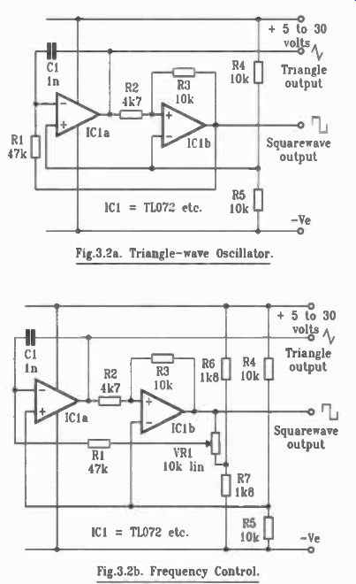
Fig. 3.2
Practical testing of this circuit with a TL072 yielded just over 1.1kHz. With a 100pF capacitor for C1 it managed 72kHz, and a TL082 was slightly faster at 79kHz. Stability with factors such as changing supply voltage was good. The frequency can be changed by altering any of the four passive components. It might be worth noting that the frequency is linearly proportional to the value of R3, so adjusting this gives a more linear range of control, but it also changes the amplitude of the triangle wave output. For reliable operation R3 should always be greater than 1.5 times the value of R2. Replacing R3 in Figure 3.2a with a 100k linear pot in series with an 8k2 resistor gave an adjustment range slightly greater than 1 to 10kHz.
For a reasonably linear frequency control with constant triangle wave amplitude, the modified circuit shown in Figure 3.2b can be used. This sends the output from IC1b to R1 through the variable attenuator VR1. The low end of this is given a half-supply potential by the divider resistors R6 and R7, with values chosen so that in parallel they represent slightly less than a tenth of the value of the pot. Unlike increasing the value of R3, which raises the frequency, this reduces it so C1 is reduced to In to obtain the same range of 1 to 10kHz.
Both circuits are shown for use with single supply voltages.
Where a dual supply is available, R4 and R5 will be unnecessary, the two inputs they supply can be connected directly to ground, and the low end of VR1 can also be connected to ground, perhaps through a suitable resistor to set the minimum frequency.
Components for Figures 3.2a and 3.2b
Resistors (all metal film, 0.6W)
R1 47k
R2 4k7
R3, 4, 5 10k (3 off)
R6, 7 1k8 (2 off)
VR1 10k linear carbon pot
Capacitors
C1 10n or 1n polyester or polystyrene
Semiconductors
ICI TL072
An Audio Sinewave Oscillator
Most of the oscillators described so far have been presented as simple outline circuits for use by designers and experimenters in their own projects. Extras such as power supply decoupling, output buffers and DC blocking capacitors have generally been omitted. However, this circuit can be constructed as an extremely useful general workshop test oscillator, so it is given as a complete mini-project. In Section 7, which deals with construction, full details are given for building it with a simple stripboard layout.
The design uses the "Wien Bridge" circuit to generate a sinewave output with excellent purity and it has four frequency ranges covering 10Hz to 100kHz. The output is from a 50-ohm source with an amplitude control for adjusting the level from zero to a maximum of 1 volt RMS, corresponding to about 2.8 volts peak-to-peak. The supply current is only about 12mA and a 9-volt supply can be used, making battery operation possible.
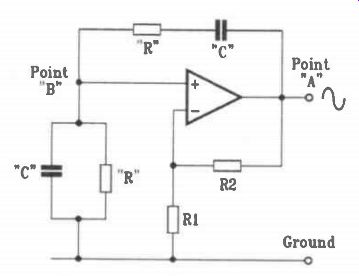
Fig. 3.3
The basic op-amp Wien Bridge oscillator circuit is shown in Figure 3.3. The bridge consists of two sections using the components "R" and "C", one with them in series, and the other with them in parallel. The junction of these two arms supplies positive feedback to the amplifier whilst negative feedback, for amplitude control, is applied through R2 and R1. The capacitors and resistors of a Wien Bridge are usually of equal value, so that when a sinewave is applied to the point "A" in the figure the feedback signal at point "B" will only be in phase with it at the frequency given by the formula:
f - 2 x n x RxC 1
This determines the frequency of oscillation since the positive feedback must be in phase for it to work. To allow variation of the output frequency the two resistors are often made variable by using a dual-ganged pot.
There's a snag to this delightfully simple circuit of course.
Isn't there always? At the working frequency the positive feed back voltage at point "B" is exactly a third of that applied to point "A", so the amplifier must have a gain of exactly three to sustain the oscillation. The tiniest fraction more and the amplitude rises until the amplifier output "clips"; a tiny bit less and the oscillation simply dies away. This means that automatic gain control is necessary to sustain the oscillation at a reason able level. This control usually has to cover quite a range too, to cope with the mismatches common between the two sections of most ganged pots. Descriptions of this type of circuit often state that the control should act slowly to minimize distortion, especially at low frequencies. They don't usually mention the way in which the rate of operation of the gain control can clash with the rate of the output amplitude's response to it, frequently causing violent instability! Since the Wien Bridge oscillator was invented circuit designers have been struggling to control it, using everything from tungsten lamp filaments and expensive thermistors to LDRs (light dependent resistors) and FETs (field effect transistors) as gain controls.
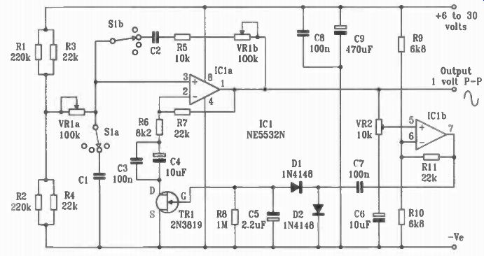
Figure 3.4. Wien Bridge Oscillator Circuit.
A field-effect transistor (FET) is relatively simple to use for control so it was chosen for this project. The full circuit of the oscillator is shown in Figure 3.4. The two sections of the bridge use capacitors C1 and C2, with 100k variable resistors and 10k fixed resistors to set the range of just over ten-to-one. For the parallel section, the 10k fixed resistance consists of the four resistors RI to R4 which also act as a potential divider to set the DC working point to half the supply voltage, as this circuit is designed to work from a single supply voltage. Their combined resistance is 10k.
Most of the negative feedback is set by resistors R6 and R7, with the FET TR 1 used to adjust the precise value. Over a limited range of gate * voltage, a junction FET behaves like a variable resistor. The signal voltage across it should be kept low, to about 100mV peak-to-peak, when doing this to avoid distortion. In this circuit R8 initially biases the FET on, increasing the gain of IC1a so that oscillation begins. The oscillator output is amplified by IC lb and rectified by diodes D1 and D2 to produce a negative voltage at the gate of TR 1, increasing its resistance to lower the gain of IC 1 a and reduce its output amplitude. The precise point at which a balance is struck is adjusted with VR2 to suit the particular FET used. If the output is set to about 1 volt peak-to-peak the voltage across the FET will be about 100mV. Once adjusted, the amplitude stays substantially constant right across the frequency range of the circuit and hardly varies at all with changes of supply voltage from six to thirty volts, allowing the circuit to be operated from unregulated battery supplies. Below about 50Hz the amplitude does rise slightly, to a maximum of about 50% over the set level at 10Hz, due to the higher impedance of C7 at low frequency.
This range could be omitted for audio work, or the values of C7 and C5 could be adjusted for this range.
The four frequency ranges are set by four pairs of capacitors for C1 and C2, selected with the range switch S1, giving coverage from 10Hz to 100kHz. For clarity only one pair is shown, but the table below shows the values required.
Several dual op-amps were tried in this circuit and most worked well. The best was the 5532, which reached the maximum frequency of 100kHz with ease, but the TL072 worked almost as well, to 97kHz. The TL082, LF353, 4558 and 3240 all gave reasonable performance. Devices to avoid are the LM358 and the 1458 as both of these are much too slow. The output amplitude rises slightly below about 40Hz, but is otherwise stable and settles to the working level rapidly following changes of frequency, etc.
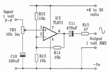
Fig. 3.5
The output of 1 volt peak-to-peak is a little low for general purpose use, so it can be raised to 1 volt RMS, just below three volts peak-to-peak. Figure 3.5 shows a circuit for this. The "level" control VR3 sets the input to IC2, a TL071 arranged to give a voltage gain of three. The DC blocking capacitor C11 allows the output to be used with the negative supply rail as "ground" whilst resistor R15 gives it an output resistance of just below 50 ohms. This part of the circuit is adjusted by set ting the frequency to around 500Hz, turning the output level up to maximum, connecting a test meter to it and adjusting VR3 for 1 volt AC.
Values for C1 and C2:
Capacitance Frequency Range
150pF 10 - 100kHz.
1.5n 1 - 10kHz
15n 100Hz – 1-kHz
150n 10 - 100Hz
These capacitors should be polystyrene or polyester types.
Components for Figures 3.4 and 3.5
Resistors (all 1% metal film, 0.6W)
R1, 2
R3, 4, 7, 11
R5, 12, 13, 14
R6
R8
R9, 10
R15
VR1
VR2
VR3
Capacitors
C1, 2
C3, 7, 8
C4, 6
C5
C9, 11
C10
Semiconductors
D1, 2
TR1
IC 1
IC2
Miscellaneous
S1
220k
22k (4 off)
10k (4 off)
8k2 1M
6k8 (2 off)
47 ohms
100k linear carbon dual-ganged type
10k horizontal "cermet" preset.
10k linear carbon see table
100n resin-dipped ceramic (3 off)
10µF/50V radial lead electrolytic (2 off)
2.2µF/100V radial lead electrolytic
470µF/35V radial lead electrolytic (2 off)
100e/35V radial lead electrolytic
1N4148 silicon signal diode (2 off)
2N3819 N-channel
J-FET NE5532N dual op-amp
TL071 op-amp
Switch, 2-pole 4-way.
Also see: