The 8038 Function Generator IC
To round off the subject of oscillators using resistors and capacitors to control frequency, a couple of dedicated "function generator" ICs will now be described. The name "function" indicates that they produce more than one output waveform, and they are often referred to as "waveform generators". Sometimes just square and triangle waves are available, but at the time of writing two readily available devices can also produce sinewaves, which can be useful in some designs. Both work in the same way, charging and discharging an external capacitor with constant current and switching the current polarity at preset voltage levels to generate the squarewave and the triangle, and processing the triangle with an internal "shaping" network to obtain the sinewave. From the designer's point of view though, there are some important differences between them.
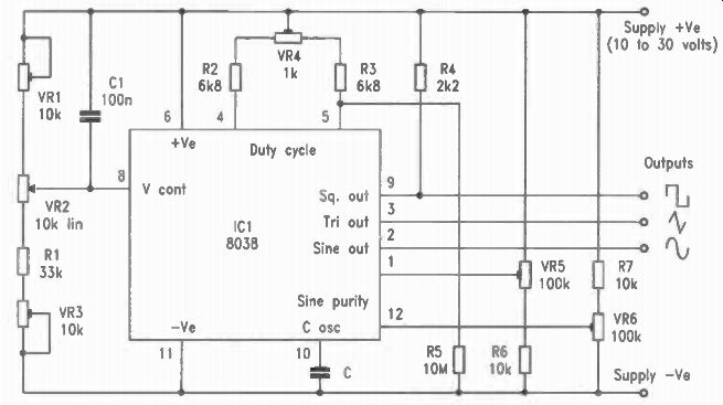
Fig. 4.1. Basic Connections for the 8038 Function Generator.
The earlier device, the 8038, has been around for some years now. It's relatively cheap but a little complicated to use.
Maximum frequencies of up 1MHz are claimed for it depending on which manufacturer's data sheet is available. In fact if a reasonably pure output is required it is best not to exceed 100kHz, with an absolute maximum of 200kHz if some distortion at the top end is tolerable. The minimum supply voltage for this device is 10 volts with a maximum of 30 volts, and as it consumes around 20mA it is probably better to forget battery operation and use a mains-powered 20 volt supply.
A general purpose circuit for operating the 8038 is shown in Figure 4.1. A brief description of some of the pin functions should assist experimenters to understand how the IC works.
The current flowing into pin 4 controls the rising part of the triangle wave, whilst current flowing into pin 5 controls the falling part. Varying the ratio of these two therefore varies the duty cycle and can be used to produce sawtooth and pulse waveforms, although this is outside the scope of this section.
For a reasonably pure sinewave some duty-cycle minor adjustment is usually necessary, this being given by the preset VR4. Also for optimum sinewave purity two further preset adjustments can be made to pins 1 and 12 by VR5 and VR6.
This calls for a method of indicating the output distortion though, so if this is not available or maximum possible purity is not required, they can be omitted with pin 1 left unconnected and pin 12 connected to negative rail through an 82k resistor.
All three outputs are available simultaneously. The triangle is provided from pin 3, the sinewave from pin 2 and the square wave from pin 9. The squarewave output is sourced from the collector of an internal transistor which can sink current to ground but not supply it so the "pull-up" resistor R4 is required.
There is an inevitable conflict between power consumption and speed here. The falling edge of the squarewave is fast as it is actively pulled down by the transistor, but the rise time will be slower since it is set by the time constant of the resistor combined with stray and transistor collector capacitance. The lower the resistor the faster the rise time, but the heavier the current whilst the transistor is on. Note that the resistor doesn't have to be returned to the main positive supply. It could, for instance, be connected to a separate 5-volt logic supply to generate a ITL-compatible output. The amplitude levels of the three outputs differ, the squarewave being practically supply voltage peak-to-peak, the triangle about a third of this and the sinewave about a fifth. The average DC value of all the outputs is always exactly half the supply, so if a split supply is used they will be symmetrical about "ground". In addition to the resistors connected to pins 4 and 5, the frequency is set by the capacitor between pin 10 and ground and it can be varied by a voltage applied to pin 8. The capacitor is usually chosen to set the range using values from 100pF up to 100µF or more. Electrolytics can be used, though the wide tolerance of their values means individual selection will probably be necessary. The table shows values of "C" which can be used with the circuit shown to build the "front-end" of an inexpensive 2Hz to 200kHz general purpose function generator. The control voltage from VR2 sweeps the output across the selected range, and with the values shown it can be set up to give a 10-1 ratio. Note that the action of VR2 is inverted as the lower the control voltage, the higher the output frequency.
Values of "C" for various frequency ranges:
Capacitance Frequency
200pF 20 to 200kHz
2.2n 2 to 20kHz
22n 200Hz to 2kHz
220n 20 to 200Hz
2.2µF 2 to 20Hz
Capacitors should be polystyrene or polyester types.
Components for Figure 4.1
Resistors (all 1% metal film, 0.6W)
R1 33k
R2, 3 6k8 (2 off)
R4 2k2
R5 10M
R6, 7 10k (2 off)
VR1, 3 10k preset (2 off)
VR2 10k linear carbon pot
VR4 1-k preset
VR5, 6 100k preset (2 off)
Semiconductors
ICI 8038 waveform generator.
The MAX038 Function Generator
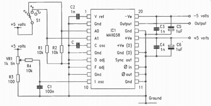
Fig.4.2. Basic Connections for the Maxim MAX083 Function Generator.
The second "function generator" device to be described is a relative newcomer to the market, in fact it was released during the preparation of this guide. This is the Maxim MAX038, which is probably destined to replace the older device as the industry standard waveform generator. Whilst it also provides triangle, square and sinewave outputs, there are many differences which designers and experimenters should know about.
In some ways it is a lot easier to use than its predecessor, but in others it can prove more difficult. The single most important difference is that it is capable of much higher frequencies so careful layout is needed to ensure stable, low distortion output.
The MAX038 requires dual power supplies of plus and minus 5 volts with a tolerance of plus or minus a quarter of a volt. It draws around 50mA from each, so once again it is better to forget batteries and provide power with a transformer and a couple of 3-terminal 5-volt regulators. Although within the current rating of the TO92 packaged regulators, the supply currents will probably cause excessive heat dissipation so l amp types 7805 (positive) and 7905 (negative) are preferable, fitted with small heat sinks. An additional advantage of mains power is that if the designer wants to process the output using op-amps, the supply can be constructed to provide 12 or 15 volt dual outputs for these too.
The IC itself is contained in a 20-pin DIL package. This number of connections may seem daunting until it is realised that six of these are "ground", and for many applications some of the others will not be needed either and can be left open or grounded as appropriate. There are generally less external connections to be made than with the 8038. Figure 4.2 shows the basic circuit needed to get a MAX038 up and running to generate sine, square and triangle outputs. The first point to note is that the positive and negative 5-volt supplies, to pins 17 and 20 respectively, have local decoupling capacitors to ground placed very close to the pins. For each supply this consists of a le ceramic or tantalum bead capacitor, and where tantalums are used there should also be 1 n ceramics in parallel with them.
Unlike the 8038, the output waveform is selected internally, controlled by the logic levels applied to pins 3 and 4. Logic "low" is ground, not negative, whilst logic "high" is positive 5 volts, so selection could be made directly by a digital circuit.
For most applications an external switch will be used and the arrangement shown, with two "pull-down" resistors R1 and R2, is about the simplest possible. Leave the two inputs unconnected and they'll both be pulled low by these resistors and the output will be a squarewave. Pull only pin 4 high and the triangle wave will appear at the output. Pull pin 3 high and the output will be the sinewave, regardless of the state of the other two, which is useful if both are accidentally made positive during switching. The single-pole three-way switch Si thus determines the waveform, and because no high frequency signals pass through it, wiring layout to it is non-critical. The output, from pin 19, has a constant amplitude of 2 volts peak to peak for all three waveforms and a very low output impedance which simplifies the design of following circuitry considerably in comparison with the 8038.
The frequency is controlled by the value of the capacitor "C" between pin 5 and ground and the current flowing into pin 10.
The capacitor can have any value between about 20pF and 100e or more. It should be placed so that the ground connection is close to pin 6. A small trimmer can be used together with a fixed capacitor to compensate for stray capacitance for high frequency ranges. Although never really a good choice for timing and frequency generation circuits, an electrolytic can be used, with the positive end towards pin 5, as the IC charges and discharges it between zero (ground) and one volt positive.
The output frequency is linearly proportional to the current flowing into pin 10, for values between 2µA and 7501.1A. Since pin 10 is always at ground potential, all that is needed to provide a linear controlled current is a variable voltage and a resistor. For many applications the arrangement shown in Figure 4.2, with VR1 and R3 setting a ten-to-one voltage range and R4 to convert it to a current, will be all that is needed. The frequency is given theoretically by: Input current I, Capacitance C which is much simpler than many of the other circuits in this guide. The output actually produced conforms closely to this formula for most values of I and C. The IC is normally specified as capable of operating up to 20MHz. At this frequency there is some apparent distortion, but at 10MHz the sine and triangle waveforms are excellent and even the squarewave is still recognizably rectangular.
Now for a few cautions and "don't’s”. Pin 1 is a reference voltage output of 2.55 volts from an internal "bandgap" source, intended for use in generating input currents. The data sheet says it can supply up to 4mA, but neither of two examples tested by the author managed more than 1-mA. Greater loading than this caused a drop in the reference voltage. This is much worse news than at first appears because this reference is also used by internal circuits of the chip. If it is pulled down the frequency rises, the output amplitude dips, and heavy distortion occurs in sine and triangle outputs. It is probably better to provide this pin with a in ceramic decoupling capacitor as shown and otherwise leave it alone. It could be buffered with an op-amp, but since a regulated 5-volt positive supply should already be available at much higher current, why bother? The next point to watch out for is the action of an internal comparator, with a 5 volt output available from pin 14 which can be used to provide a logic-level synchronizing signal. The output of this has very fast rise and fall times and unless great care is taken with layout, using a double-sided "ground-plane" PCB, it has a tendency to find its way through stray capacitive coupling to the main output, causing distortion and spikes. It has a separate positive power supply at pin 16, so if it is not needed this can be left unconnected to disable it. However the "digital ground" at pin 15 should be connected to ground, otherwise the comparator's input circuit will still cause severe distortion.
Figure 4.2 shows all that is required to get this IC working to generate clean 2-volt peak-to-peak outputs all the way up to 10MHz and beyond. There are other features available of which designers should be aware, although a full description is beyond the scope of this guide. Pin 7 is a "duty cycle adjust" input which, if supplied with a voltage between plus and minus 2.3 volts will alter the duty cycle from 15% to 85% whilst having practically no effect on the frequency. This can be used to generate sawtooth or pulse waveforms. Connecting it to ground as shown results in a 50-50 duty cycle. Pin 8 is a "frequency adjust", which, when fed with a similar control voltage, will vary the output frequency between 0.3 and 1.7 times its nominal value. The obvious applications for this are frequency sweeping or a "fine tune" control. This too can be grounded if not required. Both these inputs have internal 250µA current sinks to the negative supply so they should never be left unconnected. If they are supplied through resistors, the effect of these currents must be allowed for. Finally, there is an on-board phase comparator which can be used for synchronizing the output frequency to another signal. This has an input to pin 13, and an output from pin 12. With suitable filtering it can supply a voltage to pin 8, the "frequency adjust" input, for true phase locked loop operation.
Provided the layout considerations are kept in mind, this is actually a much easier device to use than the 8038. There are less preset adjustments to be made, control is simpler and more accurate and the performance is superior in just about every way. The sinewave output in particular is very good, even at high frequency, much better than it's predecessor. The price is a small snag at the time of writing, but at around $25.00 it is not really prohibitive and in time will probably fall considerably.
Values of "C" for various frequency ranges:
Capacitor Frequency range
22pF 1 to 10MHz
220pF 100kHz to 1MHz
2.2n 10 to 100kHz
22n 1 to 10kHz
220n 100Hz to 1kHz
2.2µF 10 to 100Hz
Capacitors should be polystyrene or polyester types. A trimmer can be used for the highest range.
Components for Figure 4.2
Resistors (all 1% metal film, 0.6W)
R1, 2, 4 10k (3 off)
R3 100-ohm
VR1 1k linear carbon pot
Capacitors
C1 100n ceramic
C2, 3, 4 in ceramic
C5, 6 le/35V tantalum bead
Semiconductors
IC1 MAX038 waveform generator. (Maxim).
Also see: