LC Oscillator Circuits
In this section circuits are given for some oscillators using resonant coil and capacitor combinations to determine frequency. Whilst this type tends to be restricted to circuits operating at radio frequencies, there is no reason why this should always be so. Many component suppliers now offer useful ranges of small inductors, either as tiny potted ferrite devices or wire-ended "chokes" which are very similar in appearance to resistors and using these, it is possible to generate frequencies down into the audio range. The output frequency is generally far more stable than that of the CR circuits describes so far, especially at high frequencies, and may provide a useful alter native to crystals in many frequency-generating circuits.
Though not as easy to tune as CR circuits, they are much better than crystals in this respect. For experimenting, the inductors are cheaper than crystals and can be tuned to a wide range of frequencies by selection of the capacitors used with them.
Whilst low frequencies could use large inductors and capacitors, a useful alternative technique is to reduce the high frequency of an LC oscillator with a CMOS divider, resulting in a very stable low frequency. The entire process can frequently be done by a single inexpensive IC. Many designers find a mental picture of the circuit action is a help when designing, both in figuring out what is happening if it fails to perform as expected and in creating fresh versions of it. One way of doing this is to use the "water analogy", where the flow of current is compared to the flow of water along a pipe with the voltage being seen as the pressure driving it.
Using this comparison, an inductor can be thought of as a mass of water flowing in a long pipe, its inertia causing it to take up (or release) energy with any change in speed. A capacitor in such a system would consist of a wide section of pipe with a rubber diaphragm placed across it, which would prevent a steady flow (DC) but would allow an oscillating movement (AC), the amount depending on the pressure and stiffness of the diaphragm.
If the ends of these two hypothetical devices are connected together the result will be the equivalent of a parallel LC "tank" circuit. If the water in the pipe is given an initial push it will bounce back and forth as its inertia reacts with the springiness of the diaphragm. This is similar to current in the electrical circuit. Friction in the pipe will cause the oscillations to die away and eventually stop, again a useful comparison as oscillations in the electrical circuit usually lose power mainly because of resistance in the coil. If a way is found to sense the water movement and give it a suitably timed nudge during each cycle the system becomes an oscillator, just like the electrical version.
All too often LC oscillator circuits give disappointing results when constructed. They may distort, burst into unwanted parasitic frequencies, or simply fail to work at all. This is often caused by coil characteristics, which are not as easy to deter mine as those of resistors and capacitors. Coils may be anything from high-Q inductors on ferrite pot cores, through home wound items on bits of ferrite rod to air-cored types with very few turns. Circuits with high operating frequencies often use a single transistor or FET for sustaining the oscillation in place of the op-amps and CMOS gates found elsewhere in this guide.
The component values used in such circuits often need "tweaking" to obtain optimum performance, requiring suitable test equipment to examine the results. The aim in this section is to provide a number of circuits, using both discrete devices and CMOS gates, that have proved to be fairly reliable with various frequencies and coil types. Most of the transistor and FET types are capable of low distortion, though an oscilloscope may be needed for adjusting this. The CMOS types by their nature contain square waves somewhere in the circuit, but they are simple, very reliable, and the waveform across the LC tank circuit is often fairly "clean".
Coil and Capacitor Values
All the circuits of this section use "parallel-resonant" tuned circuits to fix the operating frequency. At resonance, the reactances (AC impedances) of the inductance and the capacitance are identical (although opposite in sign). For any resonant frequency there is a large number of inductor and capacitor combinations that could be used so one problem is to decide which of the many possible values will be most suitable.
In the water-based equivalent, the main source of loss was friction in the pipe. This suggests that the less actual movement takes place, the less the friction losses will be. This points to use of a lot of water and a stiff diaphragm so that most of the energy movement will be in the form of pressure change instead of motion. The electrical equivalent is, within reason able limits, a large inductance and a small capacitance. How large, and how small? Guidance on this point is hard to find, but in general the author has found that selecting values of L and C to have impedances of about 1000 ohms at the operating frequency will usually give reasonable results. This is a very rough guide and use of components having several times this value, or a small fraction of it, will often have little effect on oscillator performance. However, it does at least provide a starting point for design.
The formulae for LC oscillator calculations are quite simple.
The reactance of a capacitor is given by:
1 2 xitxfxC
Where f is the frequency in hertz of the applied voltage and C is capacitance in farads.
The reactance of an inductance is given by: 2 xicxfxL
where f is again the frequency, and L is the inductance in henries.
Normally the values of C will be in picofarads (pF) or nanofarads (nF), and the inductance in millihenries (mH) or microhenries (µH). Many calculators allow direct entry of the necessary "powers-of-ten" for such calculations.
At resonance the results of the two above formulae are equal for the components in use. Some rearrangement therefore shows that at resonance, the frequency is given by:
1 f = 2xnx1r1.-- x -C -
The units again being hertz, henries and farads. With a little practice these calculations become very easy to perform.
For some applications constructors might like to construct their own coils. This is a bit of a trial-and-error procedure as various types of ferrite have different characteristics, but as a very rough guide 50 turns of 0.4mm enameled copper wire on a length of 9mm diameter ferrite rod should have an inductance of about 250 uH. A point to note is that the inductance is proportional to the square of the number of turns. Therefore, if a value of 500 µH is needed, the turns should not be increased to 100 turns, instead the figure would be:
√(500/250) x 50 = 70.71
so somewhere around 70 turns is needed. This applies to most coil types, though inductance also varies with length along the axis, permeability of the core material, diameter of the wire and so on. Coil winding is an area where there is no substitute for practical experiment.
Transistor Hartley Oscillator
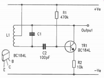
Fig. 5.1. Transistor Hartley Oscillator.
All oscillator circuits need positive feedback in order to sustain oscillation. To suit the amplifying device used, the feedback signal may need a change in level or impedance and, as in the case of a transistor circuit where it is taken from the collector and applied at the base, it may need polarity inversion. This is often achieved by using a "tap" in the tuned circuit. Some of the basic LC oscillator circuits are named after the engineers who originally thought of them, and the main difference between these is often the way in which the tank circuit is tapped. With the Hartley circuit, the coil is tapped. This is easy enough to provide in the case of home-wound coils, making this a useful circuit for use when experimenting with RF signals.
If the coil is thought of as a simple transformer, it will be seen that if the tap is grounded, then a positive polarity excursion applied to one end will result in a negative one at the other, and vice-versa. The tap can provide a voltage or impedance change if there is a difference in the number of turns to each side of it, though in many simple circuits it is sufficient to use a centre-tap. In the circuit of Figure 5.1 the collector current of transistor TR1 flows through one half of the coil to the positive supply rail, and the positive feedback taken from the other is applied to the base through DC blocking capacitor C2.
Capacitor C1 combines with coil L1 to set the resonant frequency, and can be a variable type as used for tuning AM radios. The version tested used 60 turns of 0.4mm enameled copper wire close-wound on a 9mm diameter ferrite rod and when tuned with a 5-240pF variable capacitor for C1 covered a range of 0.6 to 1.6MHz with a reasonably pure output wave form. This is approximately the AM radio medium wave range, so the circuit can be used for testing such radios.
The Hartley is a lively oscillator which easily produces high signal voltage levels but is prone to distortion though overdriving of the resonant circuit. The resistor R2 in the emitter circuit provides negative feedback which controls amplitude and distortion to some extent, and this may need some adjustment when used with other coil and capacitor combinations.
There are two disadvantages with this version of the Hartley circuit. One is that neither end of the tuning capacitor is grounded, so in tune-able RF circuits it may be susceptible to the effect of stray capacitance from the user's hand. The other is provision of the coil tap. This is simple with home-wound coils but commercial inductors, chokes and the like may not have suitable taps. One possibility is to use two coils in series, so long as they are positioned so that their magnetic fields do not oppose each other significantly. At first sight it appears that this might not work but in practice it usually does, probably because the resonant CR network is still "prodded" by the transistor sufficiently to provide the necessary feedback.
Components for Figure 5.1
Resistors (all metal film, 0.6W)
R1 470k
R2 10k (but see text)
Capacitors
C1 see text
C2 100pF polystyrene (could be increased for lower frequencies)
Coil
L1 see text
Semiconductor
TR1 BC184L (although most small silicon NPN transistors should work in this circuit)
Transistor Colpitts Oscillator
To avoid the need for a tapped coil, it is possible to tap the capacitor of the resonant circuit instead. Although it may not be immediately apparent, this in fact has exactly the same effect as a tap on the coil and can be used in the same way. Like the Hartley this type of circuit is named after its inventor, an engineer by the name of Colpitts. Apart from removing the need for a tapped coil, the Colpitts oscillator is less lively than the Hartley and so can more easily be used for generating a signal of reasonable purity, so it is often found in RF signal generators.
There are now two tuning capacitors however, and since they are in series their effective capacitance is reduced. For tune-able versions of the Colpitts, variable capacitors having two equal sides can be obtained. At one time large and solidly constructed air-spaced tuning capacitors were commonplace and many constructors may still have at least one of these, possibly salvaged from the stripping of an old radio. New ones can still be purchased from some suppliers, though their price tends to be a trifle prohibitive. However, there is no reason why one of the small and cheap plastic-cased types should not be used instead. The tap between the capacitors is connected to ground, thereby eliminating the stray capacitance problem of the previous circuit.
A single-transistor version of the Colpitts circuit is shown in Figure 5.2. For fixed frequency operation, wire-ended chokes or tiny inductors can be used in this circuit together with fixed capacitors. It would then also be possible to vary the ratio of the capacitor values to experiment with impedance matching, possibly increasing C2 with respect to C1 to reduce the drive input to the base of TR1. As in the previous circuit, the emitter resistor R3 controls the amplitude and purity of the output. For some combinations of L and C it may be necessary to use a capacitor to bypass all or part of this resistor, and the amount could be made adjustable by using a preset resistor to obtain optimum results. The inset next to R3 shows how this can be done. When calculating the operating frequency of this circuit, remember that the value of "C" is now that of C1 and C2 in series, which is given by:
C = 1 / 1/ C1+ 1/C2
where C 1 and C2 are equal in value, the equivalent capacitance is half the value of one of them.
Components for Figure 5.2
Resistors (all metal film, 0.6W)
R1 470k
R2 4k7
R3 2k2
Capacitors
C1, 2 see text
C3 100n polyester
Coil
L1 see text
Semiconductor
TR1 BC184L NPN silicon
Transistor Colpitts, Emitter Feedback
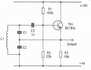
Figure 5.3
The version of the Colpitts oscillator shown in Figure 5.2 took its feedback from the collector of the transistor. To turn this into positive feedback phase inversion was needed, but only a small signal voltage as the transistor provides plenty of voltage amplification at its collector. Another version of the Colpitts circuit, Figure 5.3, often found in signal generators, obtains its feedback from the emitter. Because of the absence of voltage gain at this point this version of the circuit can often be designed to give a more pure and stable signal. The phase inversion is no longer needed with feedback from this point, but as the emitter signal voltage is always very slightly smaller than the signal applied to the base some voltage increase in the feed back is required if the oscillator is to work. Capacitors C1 and C2 again form the tap which is driven by the signal taken from the emitter of the transistor TR1. The voltage at the top of C1 is higher than the drive signal, by a factor of about two if the capacitors are of equal value, but is in phase with it for connection through C3 to the transistor base.
As with the previous Colpitts circuit the capacitors C1 and C2 may be a dual variable type, but this time their common point is not grounded, which may cause stray capacitance problems depending on the physical arrangement of the circuit.
One possibility is to use a fixed capacitor for C1 and a smaller, single-gang variable component for C2. There will be some variation in output amplitude across the frequency range if this is done though, and the coverage will be smaller. However it may be a useful option for circuits that need only a small adjustment range, perhaps for trimming purposes.
The gain of this circuit may need trimming to obtain a reasonably pure output waveform. Adjustment of the value of R3 will normally allow very good results to be achieved.
Although not shown, the Hartley circuit can also use feed back from the transistor emitter, with drive to the coil tap and a single tuning capacitor. Like its collector feedback equivalent it tends to be livelier and may need more negative feedback to obtain a low-distortion output signal.
Components for Figure 5.3
Resistors (all metal film, 0.6W)
R1 100k
R2 22k
R3 10k
Capacitors
C1, 2 see text
C3 1n polystyrene
Coil L1 see text
Semiconductor
TR1 BC184 NPN silicon transistor
Two-transistor
Oscillator
Although the circuits shown so far have been very simple, all have needed a tapping point in the resonant circuit to provide feedback. There will be many occasions when this is not convenient and a little extra circuit complexity and a second transistor can be justified to eliminate it. It is also fairly easy to modulate this design with an audio signal, as will be shown.
The basic circuit is shown in Figure 5.4a. The resonant tank circuit of L1 and C2 forms the load for the collector of transistor TR 1, and feedback is taken from here by capacitor C3 to the base of the second transistor TR2 which then completes the circuit by returning this feedback to the emitter of TR 1. It can do this since resistor R3 effectively supplies a constant current to the two emitters, so the more current TR2 draws the less is available for TR1 and its load. The bases of both transistors are supplied with a bias voltage by resistors RI and R2, but whilst C1 "grounds" the base of TR 1 at signal frequencies, R4 allows the feedback signal from C3 to drive the base of TR2.
With a 9-volt supply, the prototype of this circuit delivered an output of about 6 volts peak to peak, using the 60 turn coil wound on 9mm ferrite and a 5 to 250pF variable capacitor for C2. R3 controls amplitude and may need adjustment to suit other coil and capacitor combinations where low output distortion is needed. With a 10µH choke for the coil the output frequency ranged up to 10MHz, but R3 had to be reduced to 10k for this. At the other end of the scale a frequency of 50kHz was achieved using a 1mH choke and a 10n polyester capacitor as the resonant circuit.
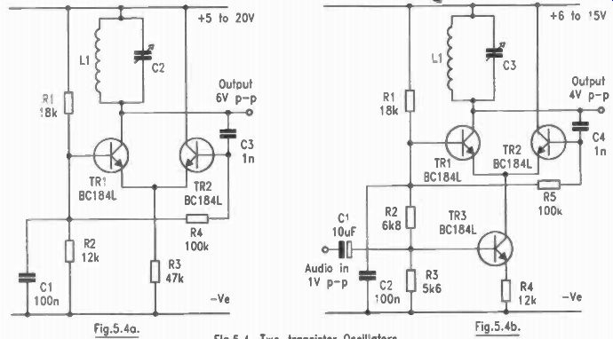
Fig. 5.4
This circuit is exceptionally reliable and will work happily with many different coil types, generally producing a good low distortion output. The tuning capacitor C2 has one side connected to the positive supply rail, which is usually equivalent to "ground" at signal frequencies so the effects of stray capacitance is minimized when a variable capacitor is being used. One final point of interest is that if a designer really needs the coil and C2 to be connected to negative supply, there is no reason why the circuit should not be constructed "upside down", using PNP transistors instead of the NPN's shown. The PNP equivalent of the BC184L is the BC214L, which has the same lead arrangement.
Components for Figure 5.4a
Resistors (all metal film, 0.6W)
RI 18k
R2 12k
R3 47k (see text)
Capacitors
C1 100n polyester
C2 see text
C3 1n polystyrene
Coil
L1 see text
Semiconductors
TR1, 2 BC184L NPN silicon transistor (2 off)
Audio modulation can be applied to this circuit quite easily.
Since the emitter resistor controls the output amplitude, it can be replaced with a transistor current source as shown in Figure 5.4b and this can be used for modulating the signal. The bias chain has an additional resistor, R3, to provide bias for this transistor. Current drawn through the emitter resistor R4 is delivered from the collector to the emitters of TR1 and TR2.
This current is dependent upon the base voltage, so it can be modulated by applying an audio signal through Cl. With a 9 volt power supply the level of the modulation signal should be about 1 volt peak-to-peak, though this may vary with different combinations of L1 and C3, and with different supply voltages.
The average output amplitude level can also be adjusted by altering the value of emitter resistor R4.
As with most simple modulation systems the output from this circuit is a mixture of amplitude and frequency modulation, but it can be used to couple a signal into a nearby AM radio with quite acceptable results for testing or perhaps using the radio as a simple audio amplifier.
Components for Figure 5.4b
Resistors (all metal film, 0.6W)
R1 18k R2 6k8 R3 5k6 R4 12k R.5 100k
Capacitors
C1 10µF/25V electrolytic
C2 100n polyester
C3 see text
C4 In polystyrene
Coil
L1 see text
Semiconductors
TR1, 2, 3 BC184L
NPN silicon transistor (3 off)
Complementary Two-transistor Oscillator
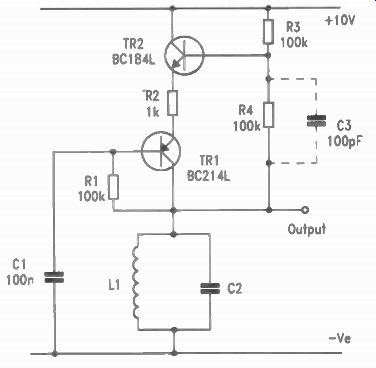
Fig. 5.5. Complementary Two-transistor Oscillator.
This interesting two-transistor circuit, shown in Figure 5.5, is similar to the one of Figure 5.4a, but this time uses transistors of complementary polarity, one NPN and one PNP. Again it is very simple and reliable, though performance is not so good when operated at higher frequencies. The version tested was found to distort a bit above 1MHz. However, it is a very good low-frequency circuit and retains the advantage of not requiring a tap in the coil or capacitor. A 1mH choke with a 100n polyester capacitor worked well, giving a frequency of just 15kHz, and there is no reason why the circuit should not work at even lower frequencies than this. A very wide range of supply voltages can be used, the test version worked quite happily with supplies from 3 to 30 volts! The resonant LC circuit L1 and C2 forms the collector load for the PNP transistor TR1 which, like TR1 of the previous circuit, has its base grounded at signal frequency by capacitor C1. Feedback and bias current is provided to the base of the NPN transistor TR2 by R3, this then controls TR1 emitter current through R2 Output amplitude can be adjusted by altering the value of R2. For maximum amplitude the feedback can be increased by the addition of C3 across R4, though practical tests will be needed to see if this is suitable with the coil being used. With a coil of reasonable "Q" and a low operating frequency, experiments showed that both R2 and C3 can be omitted altogether resulting in a very simple and economical circuit with a very good waveform, though this is not recommended with a poor "Q" or high frequency.
Like the last circuit, this one can be built the "other way up", returning the coil and C2 connections to the positive rail instead of the negative, by simply swapping the transistors. In many circuits C1 could be returned to either rail, making possible a two-terminal circuit that can be connected in series with the resonant coil and capacitor across the power supply.
Components for Figure 5.5
Resistors (all metal film, 0.6W) R1, 3, 4 100k (3 off)
R2 1k
Capacitors
C1 100n polyester
C2 see text
C3 100pF polystyrene
Coil
L1 see text
Semiconductors
TR 1 TR2
BC214L PNP silicon transistor
BC184L NPN silicon transistor
FET Hartley Oscillator
Field effect transistors also perform well in oscillator circuits.
Most of the transistor circuits described in this section have FET equivalents which are often more reliable with lower distortion. Biasing arrangements are often simpler too, and in many cases a strategically placed diode will control the gate voltage, giving automatic amplitude level control to make the output level substantially independent of supply voltage changes.
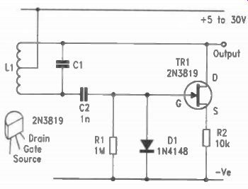
Fig. 5.6. FET Hartley Oscillator.
Figure 5.6 shows a basic Hartley circuit with the coil driven from the drain of the FET. The feedback is applied through capacitor C2 to the gate whilst resistor R2 in series with the supply to the source sets up the correct DC conditions and controls the signal amplitude. Like most N-channel field effect transistors the gate of the 2N3819 has to be biased so that it is negative with respect to the source, so if the gate is grounded and the source is provided with a series resistor the source voltage will rise until a balance is struck where the increasingly negative gate voltage prevents further increase in source current. Unlike bipolar resistors, this voltage varies quite a bit between individual FETs and circuit designs should take this variation into account. However, the arrangement shown will always bias the FET into its linear active region, allowing oscillation to start. For a given supply voltage the value of R2 could be simply adjusted for the output level required as FET circuits tend to be self-stabilizing to some extent anyway. However, the addition of the diode D1 improves stabilization further by generating a negative charge on the gate side of C2 as the amplitude of the feedback rises, and the level then remains more or less constant over a wide range of supply voltage.
The circuit shown actually ran with a supply of just 2 volts, though a minimum of 5 volts is recommended. As the supply voltage was increased the output level stabilized at about 10 volts peak-to-peak and remained constant right up to 30 volts input. With source resistors of 10k and higher the output wave form purity was excellent.
This circuit operates well up to and beyond 10MHz. The coil does require a tap of course, tests were carried out with the 60 turn home-wound coil on ferrite with a centre tap. The tuning capacitor C1 was a 5-250pF variable type. In this circuit it does not have a "grounded" side, which might cause difficulties in some applications. As with all these FET circuits other types of N-channel FET should work in place of the 2N38I9.
Components for Figure 5.6
Resistors (all metal film, 0.6W)
RI 1M
R2 10k
Capacitors
C1 see text
C2 in polystyrene
Coil
L1 see text
Semiconductors
D1 1N4148 silicon diode
TRI 2N3819 N-channel FET.
FET Hartley Oscillator, Source Feedback
Drive for the resonant LC circuit can be taken from the source of the FET instead of the drain, as shown in Figure 5.7. This usually results in lower signal amplitude across the coil, but the output waveform can be better. It also has the advantage that one end of the tuning capacitor C 1 and coil L1 is connected to ground, which can be used to minimize the effects of stray capacitance where a variable capacitor is to be used. Like the bipolar transistor version the feedback from the source does not need phase inversion, but it does need a small increase in voltage which is achieved by driving the coil through its tap with the source. The DC path for the source is through the coil, so the source resistor has been omitted and instead, the negative gate bias is generated by the diode D1. This increases as the amplitude of the oscillation builds up until a balance is reached, so the circuit has automatic level control.
With just three components in addition to the FET and the tank circuit L1 and C1, this circuit produces an excellent output waveform. The amplitude from the one tested settled at about 4 volts peak-to-peak and remained substantially constant with supply voltages from 3 to 30 volts, though this may vary with the characteristics of the FET used.. The supply current was just 50pA. It should work with a wide variety of coil and capacitor types, the prototype was tested with the 60-turn ferrite rod coil and 5-250pF tuning capacitor.
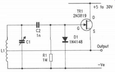
Figure 5.7
Components for Figure 5.7
Resistor (all metal film, 0.6W)
R1 1M
Capacitors
C1 see text
C2 in polystyrene
Coil
L1 see text
Semiconductors
D1 TR1 IN4148 silicon signal diode
2N3819 N-channel FET
FET Colpitts Oscillator
This is another circuit that takes its feedback from the FET drain but this time a resistor is required in the drain circuit to obtain the signal, as shown in Figure 5.8. Like the last circuit the basic arrangement has no source resistor, instead it uses the diode D1 to generate a negative gate bias across C2. However, being a Colpitts circuit, it uses an untapped coil for L1 so wire ended chokes or inductors can be used. The tuning capacitors C1 and C2 can be either fixed types or a dual-ganged variable component, in which case their common point is connected to ground. The circuit tested worked with supplies of 5 to 30 volts and generated an output of about 4 volts peak-to-peak, maintaining a fairly stable output amplitude throughout. This level may vary with the actual FET used.
A possible alternative way to stabilize it is to omit the diode and use a 10k preset resistor VR1 in series with the source, with a 100n polyester capacitor C4 connected to its wiper as shown.
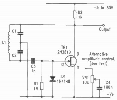
Fig.5.8. FET Colpitts Oscillator.
This can then be used to adjust the output level to some predetermined level with different FETs and coils. When set to 1 volt peak-to-peak, the output was found to be very pure and the amplitude remained constant right across the full supply voltage range. Frequencies of 10MHz and more were generated easily with this circuit.
Components for Figure 5.8
Resistors (all metal film, 0.6W)
R1 1M
R2 1k
VR1 10k (if used)
Capacitors C1, 2 see text C3 in polystyrene C4 100n polyester Coil L1 see text
Semiconductors
D1 1N4148 silicon signal diode
TR1 2N3819 N-channel FET
FET Colpitts Oscillator, Source Feedback
Two more versions of the Colpitts circuit are shown in Figure 5.9, this time driving the resonant circuit from the source of the FET. This circuit is often seen in RF signal generators, amateur HF transmitters and the like. When correctly designed, it is capable of providing a very pure, harmonic-free sinewave signal.
The first version, shown in Figure 5.9a, does not have the very best output waveform purity but has been included because it is so simple. Just a single resistor is required in addition to the resonant LC components and the FET. The version tested for this section, using a 2N3819 with assorted combinations of coils and capacitors, produced a peak-to-peak signal of almost twice the supply voltage across the coil. The waveform across the coil and capacitors was actually quite good, but if the signal is taken from the source it will probably contain some distortion due to the high drive level applied to the FET gate.
However, for a healthy output level and maximum simplicity, this circuit is hard to beat. Increasing the value of RI to 100k improves the signal waveform but reduces the amplitude to about 2 volts peak-to-peak, and for most uses it would probably require a buffer of some kind. This circuit can be operated from a wide range of supply voltages, from 5 to at least 30 volts.
An improved version is shown in Figure 5.9b. Here the feed back path to the gate of the FET has a DC blocking capacitor C3, which allows the diode D1 to generate a negative gate bias voltage in a similar manner to that of some of the circuits described earlier. This controls the amplitude of oscillation, resulting in a cleaner output signal from the FET source and a very stable output level, which may initially be set by selection of a suitable value for the source resistor. Tests showed that to avoid distortion the value of this resistor should be at least 10k, but the circuit still worked with a 100k resistor here, giving a 2 volt peak-to-peak signal across the coil and 1 volt from the source. With this value of resistor and a 10 volt supply the current taken was just 15µA, so this circuit may find applications in "micropower" designs. With a dual-ganged variable capacitor for C1 and C2 it could form a useful basis for an RF signal generator.
Components for Figure 5.9a
Resistor (all metal film, 0.6W) R 1 4k7
Capacitor C1, 2 select for frequency required (2 off)
Coil
L1 select for frequency required
Semiconductor
TR 1 2N3819 N-channel FET
Figure 5.9b
Components for Figure 5.9b
Resistors (all metal film, 0.6W)
R1 1M
R2 10k
Capacitors C1, 2 select for frequency required (2 off)
C3 In polyester or polystyrene
Coil
L1select for frequency required
Semiconductor
D1 TR1 1N4148 silicon diode
2N3819 N-channel FET
Two-FET Oscillator
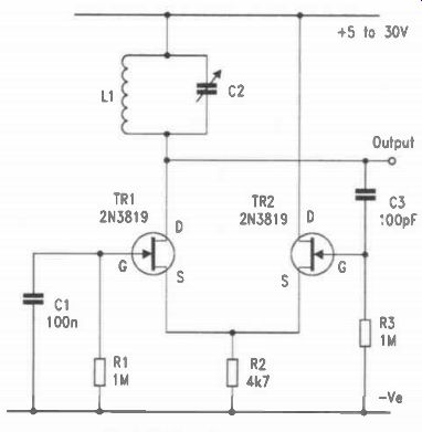
Fig.5.10. Two-FET osc.
This circuit, shown in Figure 5.10, is the FET equivalent of the 2-transistor circuit of Figure 5.4a. Like most of the FET circuits it is simpler because the biasing is less complicated and the output waveform tends to be better. Also like its bipolar counterpart it needs no taps for the feedback since this is provided, with the necessary gain, through the second active device. The high input impedance of the gate of FET TR2 allows the use of a small value for feedback capacitor C3, which reduces the load on the resonant circuit L1 and C2.
The amplitude of oscillation in this circuit can be controlled by varying the value of the common source resistor R2. A high voltage output can be achieved; with the component values shown, at a frequency of about 1MHz and with a supply of 10 volts a signal of 40 volts peak-to-peak was measured across the coil L1 whilst the current drawn from the supply was just half a milliamp. Increasing the value of R2 reduces the signal amplitude and with 100k it dropped to around 4 volts peak-to-peak.
However, with low supply voltages and a high value of R2 the circuit may sometimes fail to start up when power is applied. In general, values of R2 between 4k7 and 22k should ensure correct operation. With inefficient (low "Q") resonant circuits, values of less than 4k7 may be needed. The values of L1 and C2 will depend on the frequency required, the circuit was tried with a wide assortment of coils and capacitors, all of which worked well.
The increased complexity of this circuit makes it less suit able than some of the others for high frequency operation.
However, trials showed that it should be reliable up to at least 10MHz. Like the bipolar version, it should also be possible to add modulation by replacing R2 with a modulated current source, though the more variable characteristics of FETs would probably entail the use of a preset adjustment for the level of this.
Components for Figure 5.10
Resistors (all metal film, 0.6W)
R1, 3 1M (2 off)
R2 4k7
Capacitors
C1 100n polyester
C2 see text
C3 100p polystyrene
Coil
L1 see text
Semiconductors
TR1,2 2N3819 N-channel FET (2 off)
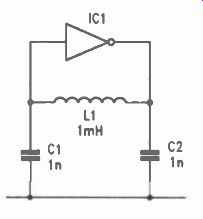
Fig. 5.11 Basic CMOS Gate Colpitts Oscillator
CMOS LC Oscillators
CMOS inverting gates can be used instead of transistors and FETs as amplifiers in the construction of oscillator circuits. Any of the usual configurations can be built with them, though in practice the simplest and most practical is probably the Colpitts circuit. Figure 5.11 shows the basic arrangement, which often will be all that is needed. The two capacitors each have one end connected to ground and it can be seen that this is actually the capacitor "tap". The usual formula can be used for calculating the frequency that will be produced, remembering that the effective capacitance is the value of both of them in series. Often they will be equal in value, so the total will be half of either of them. The example shown was tested with a 1mH choke for L1 and two in polystyrene capacitors for C1 and C2, which gave about 225kHz. With a 100µH choke and the same capacitors, it ran at just over 700kHz. The gate used was one of the four in a 4011B quad NAND gate with the two inputs connected together, though any of the CMOS inverters should work.
Apart from using just one gate, a CMOS LC oscillator built in this way gives much more predictable results than CR types at high frequencies, as the frequency depends almost entirely on the resonant components and is affected little, if at all, by factors such as the propagation delay of the device. Typically it will operate up to the maximum speed the gate is capable of, remembering that this depends to some degree upon the supply voltage. The waveform at the gate input is usually fairly pure, but at the drive end, across C2, it may show some distortion due to loading by the output of the gate. This can be improved if necessary by placing a resistor between the gate output and the junction of L1/C2. The value required will depend on the coil and capacitor in use, but something between 1k and 10k will generally be suitable.
Since other gates can be used, it follows that one of the two provided for oscillator construction in a 4060B divider will work in this arrangement. Figure 5.12 shows this with a 100µH choke and a pair of fixed capacitors C1 and C3, plus the preset trimmer C2 for fine adjustment. With the values shown the frequency will be around 1.638MHz and the trimmer will permit accurate adjustment so that the output from pin 1, the divide by-4096 output, is exactly 400Hz. When set to this with a sup ply of 10 volts, this circuit deviated by less than 1-4Hz over a supply voltage range of 5 to 15 volts, a variation of less than 0.5%. This gives some idea of the stability that can be expected. With a 220µH choke for L1 and the same capacitors, the output from pin 15 (divide-by-1024) can be adjusted to 1000Hz. With different values for L and C, this oscillator also ran happily at 5MHz with supplies as low as 5 volts, which was considerably faster than the stated performance for this IC. Should the primary oscillator frequency be needed for use else where in a circuit, the best place to obtain it is from the output of the second internal oscillator gate, which appears at pin 9.
Components for Figure 5.12
Capacitors
C1 150pF polystyrene
C2 5-65pF preset trimmer
C3 220pF
Coil
L1 100µH or 22001 miniature wire-ended choke (see text)
Semiconductor
IC1 4060B CMOS 14-stage divider with internal oscillator.
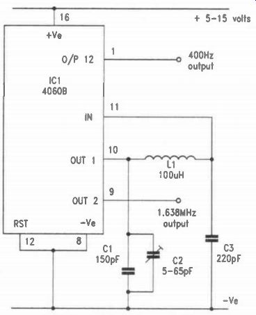
Fig. 5.12. 40608 Oscillator and Divider.
Two-gate CMOS LC Oscillator
It is possible to do away with the need for a tapped capacitor in the CMOS LC oscillator circuit by using two gates. A simple circuit for this is shown in Figure 5.13a. The resonant frequency of this is set by a single untapped coil and capacitor, which will be useful in some designs.
The output of the first gate G1 drives the input of the second G2 so that the overall phase shift of the pair is zero and feed back from the output to the input is positive. Meanwhile local negative DC feedback from the output of G1 to its input through R1 ensures that this gate operates in the active, linear state. The resonant circuit is driven through the resistor R2 and the positive feedback is taken from it through capacitor C1. This is an extremely reliable circuit that will nearly always work well even with very inefficient, low-Q coils. The author has used this in the past to drive metal detector "search coils", air-cored coils with odd shapes and diameters of 15cm or more, using three gates of a 4011B in parallel for G2 to increase power. Apart from the simplicity, the rail-to-rail resistive nature of the CMOS outputs ensured good amplitude stability, and detectors using the circuit usually gave excellent performance.
With the component values shown the circuit will oscillate at about 160kHz, though other values of L1 and C2 can be used to change this. It operates well at very low frequencies. Most of the metal detector designs operated at about 15kHz, though one experimental design used just 2.5kHz as the search frequency! The value of R2 will depend on the efficiency of the resonant circuit, but should be chosen so that the waveform across this is a fairly pure sinewave with a peak-to-peak value close to the supply voltage, which will ensure clean switching of the gates.
Too much drive will cause distortion and may affect frequency stability.
Components for Figure 5.13a
Resistors (all metal film, 0.6W)
R1 1M
R2 1k
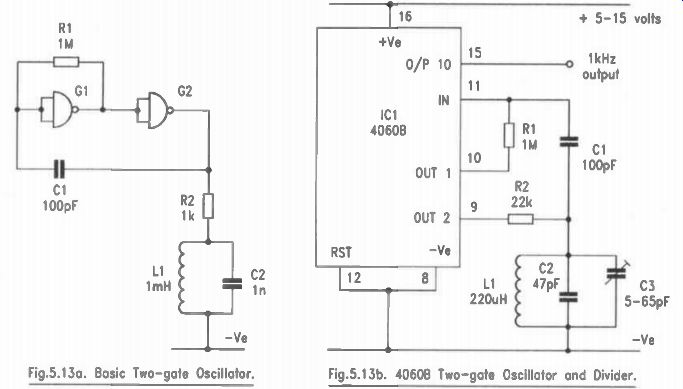
Fig.5.13a. Basic Two-gate Oscillator.
Fig.5.13b. 40608 Two-gate Oscillator and Divider.
Capacitors
C1, C2
Coil
L1
Semiconductors
G1, G2
100pF polystyrene in polystyrene 1mH (see text)
4011B CMOS quad NAND gate (any inverting gates can be used in this circuit) (2 off)
This circuit can also be implemented with the oscillator gates of the 4060B IC, as shown in Figure 5.13b. The component values shown here give an output from pin 15 that can be adjusted to precisely 1000Hz. An efficient ferrite-cored miniature inductor was used for L1 when trying this, which led to the high value used for R2. The stability was found to be not quite as good as the Colpitts version of Figure 5.12, but was still much better than a CR type. It is fairly simple to design this circuit so that it has a reasonably wide range of adjustment.
Components for Figure 5.136
Resistors (all metal film, 0.6W)
R1 1M
R2 22k
Capacitors
C1 100pF polystyrene
C2 47pF polystyrene
C3 5-65pF trimmer
Coil
L1 220µH (see text)
Semiconductors
IC1 4060B CMOS 14-stage divider with built-in oscillator.
Also see: