This information is not required in order to use the testing, adjustments and other service procedures in this guide. It is presented for those readers desiring more information about how a radio works, simply as a matter of interest or because they wish to do servicing of an advanced nature.
TUBE FUNCTIONS
The functions performed by electron tubes are many and varied, but for convenience these functions may be consolidated into a few general groups. Each function is determined not only by the tube type but also by the circuit and its associated apparatus.
A general capability of the electron tube is to alter an AC (alternating current) so that it becomes a pulsating DC (direct current), as shown in FIG. 1.
Associated apparatus can smooth out the variations in the current, and the system as a whole can be said to change an alternating current into a constant-amplitude direct current. This function provides convenient sources of DC voltage when the only available primary source of electrical energy is an AC power line or an AC generator. These DC voltages may be as low as a fraction of a volt and as high as tens of thousands of volts. The action of changing an alternating current into a pulsating direct current is referred to in general terms as rectification. The electron tube which does this is called a rectifier.
Another significant and useful capability of the electron tube, and perhaps its most important function, is described as amplification ( FIG. 2). A stronger signal voltage may be obtained from the tube than is fed into it. In effect, the tube is a signal voltage magnifier. A signal equal to 1 volt fed into the input system of the amplifying tube may appear as 20 volts at its output. Different arrangements provide for different amounts of signal amplification.
This amplification ability accounts for the advanced development of modern-day communication. It is the basis of all long distance telephony, because microwave amplifiers compensate for the energy losses encountered in transmission. Also public address systems amplify the voice of an individual so that thousands of people gathered together may hear it clearly.
Amplification makes radar possible because it strengthens the echo signal received from the target so that it can be made visible on a special screen. It is responsible for Teletype operation. Television would be impossible without it. Amplification is essential in radio transmitters and receivers of all kinds to increase electrical energy to proportions necessary for proper operation of the various circuits of the equipment.
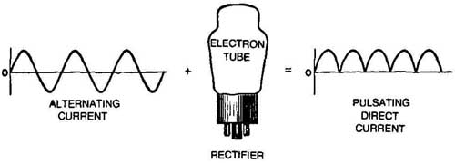
FIG. 1. Function of tube as rectifier of alternating current.
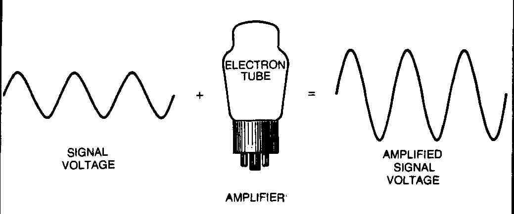
FIG. 2. Function of tube as amplifier.
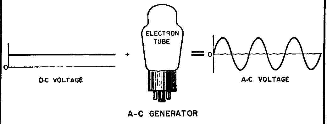
FIG. 3. Function of electron tube as generator of alternating current.
Still another extremely important facility offered by the vacuum tube is the conversion of electrical energy existing as direct current and voltage into alternating current and voltage ( FIG. 3). Used in this manner, the tube draws energy from a DC source and, in conjunction with suitable apparatus, generates high-frequency oscillations. This function has been responsible for innumerable developments in the communication field.
The principle of oscillation underlies the operation of virtually every type of radio transmitter, large or small, fixed or portable. As a generator of high-frequency oscillation, the electron tube replaced ponderous rotating machinery. Even more important is that specialized oscillators opened up the very-high- and ultra-high- frequency and microwave regions for operation. These extend from approximately 30 MHz to tens of thousands of megahertz. The use of these frequencies has helped to overcome the communication limitations caused by changing seasons and the effects of weather. It helped create new techniques, among which are radar, television and microwave cooking.
Availability of these high-frequencies for communications has made possible the convenient use of low power and the design of small receivers, transmitters and antennas.
The electron tube can modify the shape of electric current and voltage waveforms; that is, it can change the amplitude of these quantities relative to time. Voltage and current shaping (Figs. 4 and 5) are vital to the operation of numerous electronic devices. It is used in code transmission, the timing of circuit actions in radar, in the production of television pictures and in the operation of Teletype equipment. Electronic computers could not operate without waveshaping of the currents and voltages present in the equipment.
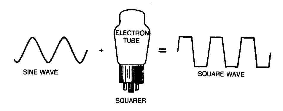
FIG. 4. One type of waveshaping accomplished by electron tubes. The input
signal is a sine wave; the output is a square wave.
At the radio transmitter, the carrier frequency is modulated by the desired signal, which may consist of coded characters, voice, music, or other types of signals. Amplitude modulation (AM) occurs if the signals cause the amplitude of the output to vary. Frequency modulation (FM) occurs if the signals cause the frequency of the carrier, or center frequency, to vary. Although there are other types of modulation, only AM receivers will be treated in this Section.
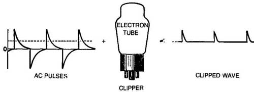
FIG. 5. Another type of waveshaping. Only parts of the positive peaks of
the input signal are present in the output.
The RF carrier wave with the modulating signal impressed upon it is transmitted through space as an electromagnetic wave to the antenna of the receiver. As the wave passes across the receiving antenna, small AC voltages are induced in the antenna. These voltages are coupled into the receiver via the antenna coupling coil. The function of the receiver is to select the desired carrier frequency from those present in the antenna circuit and to amplify the small AC signal voltage. The receiver then removes the carrier by the process of detection (rectification and the removal of the RF component) and amplifies the resultant audio signal to the proper magnitude to operate the loudspeaker or earphones.
Two major types of radio receivers are covered here—the tuned-radio-frequency (trf) receiver, and the super-heterodyne receiver.
TRF RECEIVERS
The tuned-radio-frequency receiver, generally known as the trf receiver, consists of one or more RF stages, a detector stage, one or more AF stages, a reproducer and the necessary power supply. A block diagram of a trf receiver is shown in FIG. 6. The waveforms that appear in the respective sections of the receiver are shown below the block diagram.
The amplitude of the AM signal at the input of the receiver is relatively small because it has been attenuated in the space between the transmitter and the receiver. It is composed of the carrier frequency and the modulation envelope. The RF amplifier stages amplify the waveform, but they do not change its basic shape if the circuits are operating properly. The detector rectifies and removes the RF component of the signal. The output of the detector is a weak signal made up only of the modulation component, or envelope, of the incoming signal. The AF amplifier stages following the detector increase the amplitude of the AF signal to a value sufficient to operate the loudspeaker or earphones.
RF Section
The antenna-ground system serves to introduce the desired signal into the first RF amplifier stage via the antenna coupling transformer. For best reception, the resistance of the antenna-ground system should be low. The antenna should also be of the proper length for the band of frequencies to be received, and the antenna impedance should match the input impedance of the receiver The gain of most commercial receivers, however, is generally sufficient to make these values noncritical.
The IF amplifiers in the trf receiver have tunable tanks in the grid circuits. Thus, the receiver may be tuned so that only one if signal within its tuning range is selected for amplification. When the tank is tuned to the desired frequency, it resonates and produces a relatively large circulating current. The grid of the IF amplifier then receives a relatively large signal voltage at the resonant frequency, and minimum signals at other frequencies.
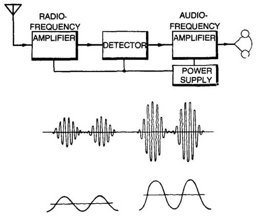
FIG. 6. Block diagram of a trf receiver and waveforms.
The relative ability of a receiver to select one particular frequency and to reject all others is called the selectivity of the receiver. The relative ability of the receiver to amplify small signal voltages is called the sensitivity of the receiver. Both of these values may be improved by increasing the number of if stages. When this is done, the tuning capacitors in the grid tank circuits are usually ganged on the same shaft, and trimmers are added in parallel with each capacitor to make the stages track at the same frequency. In addition, the outer plates of the rotor sections of the capacitors are sometimes slotted to enable more precise alignment throughout the tuning range.
Tetrodes or pentodes are generally used in if amplifiers because, unlike triodes, they do not usually require neutralization. They also have higher gain than triodes.
A typical if amplifier stage employing a pentode is shown in FIG. 7. Tuned circuit L2C1 is inductively coupled to Li, the antenna coil. R1 and C3 provide operating bias for the tube. C4 and R2 are the screen bypass capacitor and dropping resistor, respectively. The tuned circuit, L4C6, couples the following stage inductively to L3. Both transformers are of the air-core type. The dotted lines indicate mechanical ganging of C1 and C6 on the same shaft. The tuning capacitor in the next stage is also ganged on the same shaft.
If you want the receiver to cover more than one frequency range, use additional coils that have the proper inductance. They are sometimes of the plug-in variety, but more generally they are mounted on the receiver and their leads are connected to a multi-contact rotary switch. The latter method is preferable for band switching because the desired band can be selected simply by turning the switch. The same tuning capacitor is used for each band. However, when band switching is employed, the trimmers are connected across the individual tuning inductors and not across the main tuning capacitors.
Decoupling circuits are designed for both RF and AF amplifiers to counteract feedback. Thus, in the RF amplifier in FIG. 7, C5 and R3 make up the decoupling circuit. R3 offers a high impedance to the signal current, but C5 offers a low impedance. Consequently, the signal current is shunted to ground around the B+ supply. Because R3also offers a high resistance to DC current, it may be replaced by a choke coil having a high impedance only to the signal current. Each stage is similarly equipped with a decoupling circuit.
A mechanical or an electrical bandspread may be used as an aid in separating stations that are crowded together on the tuning dial.
Mechanical bandspread is simply a micrometer arrangement to re duce the motion of the capacitor rotor as the tuning knob is turned. When electrical bandspread is used, a small variable capacitor is connected in parallel with the tuning capacitor. Because of its small size, you can move this variable capacitor a considerable amount before it causes an appreciable change in the frequency of the tuned circuit. If the tuning capacitors are ganged, the bandspread capacitors are also ganged.
Detector
The process of removing the intelligence component of the modulated waveform from the ii carrier is called detection or de modulation. In the AM system, the audio or intelligence component causes both the positive and the negative half cycles of the RF wave to vary in amplitude. The function of the detector is to rectify the modulated signal. A suitable filter eliminates the remaining RF pulses and passes the audio component on the AF amplifiers.
Details of the various methods of detection will be discussed in a subsequent paragraph. Each of the several methods that might be used in the trf receiver have certain inherent weaknesses. For example, the diode detector requires several stages of amplification ahead of the detector. It loads its tuned input circuit, and therefore, the sensitivity and selectivity of the circuit are reduced. However, it can handle strong signals without overloading, and its linearity is good.
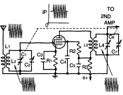
FIG. 7. An RF amplifier stage.
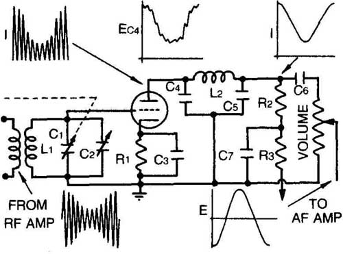
FIG. 8. Plate detector circuit.
The grid-leak detector is sensitive—and consequently requires fewer stages of amplification—but it has poor linearity and selectively. Also, it can be overloaded on strong signals.
The circuit shown in FIG. 8 employs plate detection. It has medium sensitivity and the ability to handle strong signals without overloading. The selectivity of this circuit is excellent, but because the ip:eg (plate current verses grid voltage) graph is curved near the cutoff point (where the plate detector operates), some distortion in the output cannot be avoided.
In FIG. 8, the tube is biased nearly to cutoff by the average plate current that flows through R1. This average value increases as the signal strength increases. On positive half cycles of the incoming signals the plate current varies with the amplitude of the modulating wave and produces the desired AF output voltage. On negative half cycles no appreciable plate current flows. Between positive half cycles the bias voltage is held constant across R1 by the action of C3, because the time constant of R1C3 is long compared with the time for the lowest AF cycle.
The RF pulses are filtered out by means of a low-pass filter (consisting of C4, L2 and Cs), which rejects the RF component and passes the AF component. C6 couples the AF component to the first audio amplifier. R2 is the plate load resistor, and the combination R3C7 makes up the decoupling circuit.
AF Section
The function of the AF section of a receiver is to further amplify the audio signal, which is commonly fed via the volume control to the grid of the first audio amplifier tube. In most cases, the amount of amplification that is necessary depends on the type of reproducer used. If the reproducer consists of earphones, only one stage amplification might be necessary. If the reproducer is a large speaker or other mechanical device requiring a large amount of power, you might need several stages. In most receivers, the last AF stage is operated as a power amplifier.
A necessary part of the AF section is some means of manual control of the output signal level of the receiver. A manual volume control may be employed in a number of receiver circuits. Normally this control varies the amplitude of the signal applied to the grid of an amplifier tube, as shown in FIG. 8. Increasing the resistance between ground and the sliding contact increases the amplitude of the signal applied to the grid of the driven stage.

FIG. 9. Audio amplifier output stage.
An AF output stage is shown in FIG. 9. C1 couples the first AF amplifier to the output stage, and R1 is the grid coupling resistor. R2 and C2 provide a steady bias. Because of the low frequencies involved, C2 should have a larger value of capacitance than similar bypass capacitors in the RF section. C4 is the plate-bypass capacitor, or decoupling capacitor. C3 has a small value of capacitance and bypasses some of the higher frequencies around the output transformer, thus emphasizing the bass. The impedance of the primary of the output transformer commonly represents a compromise between maximum power transfer and minimum distortion. The impedance of the secondary is chosen to match the impedance of the voice coil. Some secondaries have taps on the windings to permit an impedance match to a variety of voice-coil impedances.
Tone control is usable. The purpose of tone control is to emphasize either low or high frequencies by shunting the undesired frequencies around the remainder of the circuit components in the audio section. A simple tone-control circuit, such as the series capacitor C5 and variable resistor R3 combination shown in FIG. 9, can be connected between plate and ground or between grid and ground in any of the audio stages of a receiver. In this figure, it is connected between plate and ground. The value of the series capacitor is such that it will bypass to ground the high-frequency components. The amount of high-frequency energy removed by the tone-control circuit is determined by the setting of the variable- resistor control arm. When the resistance is low, the high frequencies are attenuated; when it is high, they appear in the output.
Feedback voltage from output to input is sometimes developed across the impedance of the common power supply. For frequencies within the usable audio range, this impedance is sufficiently low so that insufficient feedback is obtained to cause oscillation. However, for extremely low frequencies, the capacitors in the power supply will sometimes have enough impedance to cause oscillation.
When two or more audio amplifier stages are supplied from a common B+ supply, feedback occurs as a result of common coupling between the plate circuits, and some method of decoupling must be employed. The coupling consists of the internal impedance of the source of plate voltage. The feedback may either increase or decrease the amplification, depending on the phase relation between the input voltage and the feedback voltage. In a multistage amplifier, the greatest transfer of feedback energy occurs between the final and first stages because of the high amplification through the multi stage amplifier.
The effects of feedback are important if the feedback voltage coupled into the plate circuit of the first stage is appreciable compared to the signal voltage that would be developed if feedback did not exist. For example, a three-stage resistance-coupled amplifier may develop a feedback voltage (coupled via the B+ supply into the plate circuit of stage 1) which is in phase with the signal voltage of stage 1 and hence may cause oscillations to be set up. In audio amplifiers having high gain and a good low-frequency response, this regeneration causes the low-frequency oscillation known as “motor-boating.”
Design engineers usually decouple plate circuits by adding a series resistor to the input stage, between its plate load and B+, and bypassing that resistor to ground. The appearance of motorboating means you need to replace either the decoupling resistor or its bypass capacitor.
Circuit of the trf Receiver
The complete circuit of a trf radio receiver operated from an AC power supply is shown in FIG. 10. The receiver uses two pentodes in the RF section, one triode operated as a plate detector and two pentode AF amplifier stages to feed the loudspeaker.
From previous discussions, the various circuits may be identified and the signal may be traced from the antenna-ground system to the loudspeaker. The dotted lines indicate that the three main tuning capacitors are ganged on a single shaft. Across each of the main tuning capacitors is connected a trimmer capacitor to enable circuit alignment. The ground circuit and the various decoupling circuits may be readily identified. The power supply voltage is obtained from a conventional full-wave rectifier. Rectifier and tube filament currents are obtained from two low-voltage windings on the power transformer.
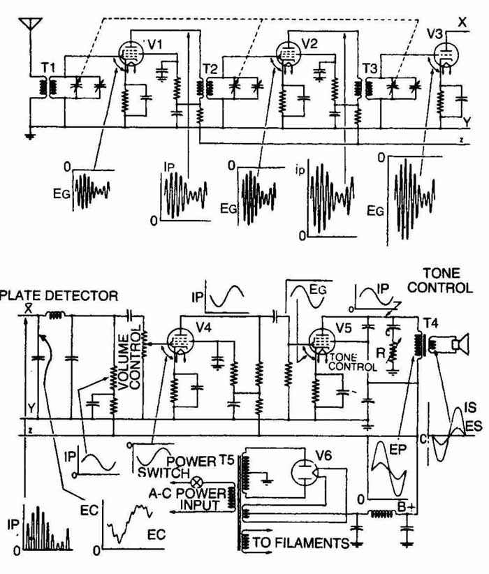
FIG. 10. Circuit of a complete trf receiver.
Characteristics of the trf Receiver
The principal disadvantage of the trf receiver is that its selectivity, or its ability to separate signals, does not remain constant over its tuning range. As the set is tuned from the low-frequency end of its tuning range to the high-frequency end, its selectivity decreases.
Also, the amplification, or gain, of a trf receiver is not constant over the tuning range of the receiver. The gain depends on IF transformer gain, which increases with frequency. In order to improve the gain at the low-frequency end of the band, RF transformers employing high-impedance (untuned) primaries are designed so that the primary inductance will resonate with the primary distributed capacitance at some frequency slightly below the low end of the tunable band. Thus, the gain is good at the low end of the band because of the resonant buildup of primary current. The near- resonant condition of the primary at the low end more than offsets the effect of reduced transformer action. However, the shunting action of the primary distributed capacitance lowers the gain at the high-frequency end of the band. To make up for the resultant poor gain at the high end of the band, a small capacitor is connected between the plate and grid leads of adjacent RF stages to supplement the transformer coupling. At the low end of the band, the capacitive coupling is negligible.
SUPERHETERODYNE RECEIVERS
The superheterodyne receiver was developed to overcome many of the disadvantages of the trf receiver. The essential difference between the trf receiver and the superheterodyne receiver is that in the former the RF amplifiers preceding the detector are tunable over a band of frequencies, whereas in the latter the corresponding amplifiers are tuned to one fixed frequency called the intermediate frequency (IF). The principle of frequency conversion by heterodyne action is here employed to convert any desired station frequency within the receiver range to this intermediate frequency. Thus, an incoming signal is converted to the fixed intermediate frequency before detecting the audio signal component, and the IF amplifier operates under uniformly optimum conditions throughout the receiver range. The IF circuits can then have uniform selectivity, uniformly high voltage gain and uniform, satisfactory bandwidth to contain all of the desired sideband components associated with the amplitude modulated carrier.
The block diagram of a typical superheterodyne receiver is shown in FIG. 11. Below corresponding sections of the receiver are shown the waveforms of the signal at that point. The RF signal from the antenna passes first through an RF amplifier (preselector) where the amplitude of the signal is increased. A locally generated unmodulated RF signal of constant amplitude is then mixed with the carrier frequency in the mixer stage. The mixing, or heterodyning, of these two frequencies produces an intermediate frequency signal which contains all of the modulation characteristics of the original signal. The intermediate frequency is equal to the difference between the station frequency and the oscillator frequency associated with the heterodyne mixer. The intermediate frequency is then amplified in one or more stages called intermediate-frequency (IF) amplifiers and fed to a conventional detector for recovery of the audio signal.
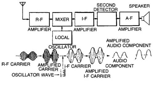
FIG. 11. Block diagram of a superheterodyne receiver and waveforms.
The detected signal is amplified in the AF section and then fed to a headset or loudspeaker. The detector, the AF section and the reproducer of a superheterodyne receiver are basically the same as those in a trf set, except that diode detection is generally used in the superheterodyne receiver. Automatic volume control or automatic gain control also is commonly employed in the superheterodyne receiver.
RF Amplifier
If an RF amplifier is used ahead of the mixer stage of a superheterodyne receiver, it is generally of conventional design. Besides amplifying the RF signal, the RF amplifier has other important functions. For example, it isolates the local oscillator from the antenna ground system. If the antenna were connected directly to the mixer stage, a part of the local oscillator signal might be radiated into space and cause interference. For this reason and others, superheterodyne receivers are provided with at least one RF amplifier stage.
Also, if the mixer stage were connected directly to the antenna, unwanted signals, called images, might be received, because the mixer stage produces the intermediate frequency by heterodyning two signals whose frequency difference equals the intermediate frequency. (The heterodyne principle is treated later in this chap ter.)
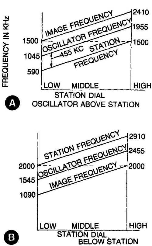
FIG. 12. Relation of image frequency to station frequency in a superheterodyne
receiver.
The image frequency always differs from the desired station frequency by twice the intermediate frequency. Image frequency is the station frequency plus or minus two times intermediate frequency. The image frequency is higher than the station frequency if the local oscillator frequency tracks (operates) above the station frequency ( FIG. 12A). The image frequency is lower than the station frequency if the local oscillator tracks below the station frequency ( FIG. 12B). The latter arrangement is generally used for the higher frequency bands, and the former for the lower frequency bands.
For example, if such a receiver having an intermediate frequency of 455 kHz is tuned to receive a station frequency of 1500 kHz ( FIG. 12A), and the local oscillator has a frequency of 1955 kHz, the output of the IF amplifier may contain two interfering signals—one from the 1500 kHz station and the other from an image station of 2410 kHz (1500 + 2 x 455 = 2410 kHz). The same receiver tuned near the low end of the band to a 590 khz station has a local oscillator frequency of 1045 kHz. The output of the IF amplifier contains the station signal (1045 — 590 = 455 kHz) and an image signal (1500 — 1045 = 455 kHz). Thus, the 1500 kHz signal is an image heard simultaneously with the 590 kHz station signal.
It may also be possible for any two signals having sufficient strength, and separated by the intermediate frequency to produce unwanted signals in the reproducer. The selectivity of the preselector tends to reduce the strength of these images and unwanted signals.
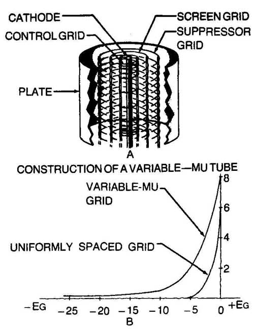
FIG. 13. Construction of variable-mu tubes and plate-current-versus-grid
voltage curves.
The ratio of the amplitude of the desired station signal to that of the image is called the image rejection ratio and is an important characteristic of a superheterodyne receiver. Better super heterodyne receivers are therefore equipped with one or more preselector stages, a typical example of which is shown in FIG. 14.
The amplification of a tube may be controlled by varying the bias voltage applied to the grid, but normally the range of this control is limited by the cutoff bias and the permissible distortion. In receivers employing automatic volume control (AVC) in the RF amplifier section, the amplification is varied over a wide range so that strong or weak signals may be accommodated. To permit this increased range of volume control, the variable-mu tube was developed. This tube is also known as the super-control or remote cutoff type.
The only difference in construction between variable-mu tubes and normal, or sharp cutoff, tubes is in the spacing between the turns of the control grid. In sharp cutoff tubes the turns of the grid wires are equally spaced, while in remote cutoff types the grid turns are closely spaced at the ends and widely spaced in the center. The construction of variable-mu tubes is shown in FIG. 13A.
With a small bias voltage, electrons flow through all the spaces of the grid and the amplification factor is relatively large because of the close spacing of the end turns of the control grid. As the bias is increased, the electron flow is cut off through the narrow spaces at the ends of the grid structure. However, they are still able to pass through the relatively large spaces at the center of the grid. The increased bias causes a decrease in the amplification due to the coarser turns in the central portion of the grid. A much greater value of bias is required to cut off the plate current flow in this type of tube. The remote-cutoff tube is so named because the cutoff bias value is greater than (more remote from) the value required to cut off plate current flow in tubes of evenly spaced turns.
FIG. 13B shows the ip:eg (plate versus grid voltage) curves for both a conventional sharp cutoff tube and a variable-mu or remote-cutoff tube. The cutoff bias for the normal tube is —5 volts, and because the slope is almost constant, any change in bias produces little change in amplification. Contrasted with this characteristic, the curve for the variable-mu tube has a pronounced change in slope as the grid bias is increased from —10 volts to —15 volts and a small value of plate current is still flowing at a bias of —25 volts. The changing slope of this curve indicates a variation of amplification with bias. Thus, if a variable-mu tube is used with a bias source that varies with the signal strength, (AVC bus in FIG. 14), the output signal can be made substantially independent of the input signal strength.
The preselector stage shown in FIG. 14 employs a variable-mu tube and cathode bias. L1 is the antenna coil, L2 and C1 make up the tuned input circuit and C2 is the trimmer used for alignment purposes. The dotted line indicates ganged tuning capacitors. Usually these are the tuning capacitor of the mixer input tank circuit and the local oscillator tuning capacitor. C3 provides low-impedance coupling between the lower end of the L2 and the grounded end of C2, thus bypassing the decoupling filters in the automatic volume control (AVC) circuit. (Automatic volume, or automatic gain, control is treated later in this Section.) The RF transformer in the output circuit consists of an untuned high-impedance primary, L3, and a tuned secondary, L4, which resonates with tuning capacitor C5 at the station frequency. The RF bypass capacitor, C6, serves a function similar to that of C3.
First Detector
The first detector, or frequency-converter, section of a superheterodyne receiver is composed of two parts—the oscillator and the mixer. In many receivers, particularly at broadcast frequencies, the same vacuum tube serves both functions, as in the pentagrid converter shown in Fig.11-15. The operation of the tube may be simplified somewhat if both stages (oscillator and mixer) are considered as exerting two different influences on the stream of electrons from cathode to plate. These electrons are influenced by the oscillator stage (grids 1,2 and 4) and also by the station input signal on grid number 3. Thus, coupling between the input signal and the oscillator takes place within the electron stream itself.
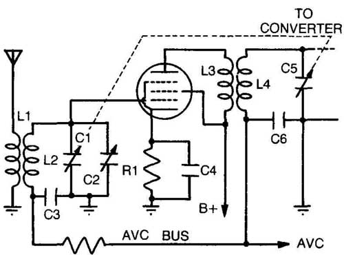
FIG. 14. Typical superheterodyne preselector stage.
There is a tendency for the local oscillator to synchronize with the station frequency signal applied to grid 3. At high frequencies where the two signals have nearly the same frequency, the pentagrid converter is replaced with a mixer tube and a separate oscillator tube. This type of circuit provides frequency stability for local oscillator.
The oscillator stage employs a typical Hartley circuit in which C5 and the oscillator coil make up the tuned circuit. C4 is the trimmer capacitor used for alignment (tracking) purposes. C3 and R2 provide grid-leak bias for the oscillator section of the tube. Grid 1 is the oscillator grid, and grids 2 and 4 serve as the oscillator plate. Grids 2 and 4 are connected together and also serve as a shield for the signal input grid, number 3.
Grid 3 has a variable-mu characteristic and serves as both an amplifier and a mixer grid. The tuned input is made up of L1 and C1, with the parallel trimmer C2. The dotted lines drawn through C1 and C5 indicate that both of these capacitors are ganged on the same shaft (in this example with the preselector tuning capacitor). The plate circuit contains the station frequency and the oscillator frequency signals, both of which are bypassed to ground through the low reactance of C6 and C7. The heterodyne action within the pentagrid converter produces additional frequency components in the plate circuit, one of which is the difference frequency between the oscillator and the station frequency. The difference frequency is the intermediate frequency and is developed across C6 and L2. This signal is coupled to the first IF amplifier grid through the desired band-pass coupling which is wide enough to include the sideband components associated with the amplitude-modulated signal applied to grid 3 of the pentagrid converter.
The conversion gain in a pentagrid converter is:
u=V_d x S_c
where Vd is the AC plate resistance with the station RF carrier applied, and Sc is the conversion transconductance (30 percent to 40 percent of the gm of the pentode amplifier). Conversion gain is the change in plate voltage at the intermediate frequency divided by the change in grid voltage at the RF station frequency for equal changes in plate current at the intermediate frequency. Expressed as a formula:
conversion gain = IF output volts/RF input volts
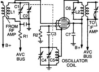
FIG. 15. First detector employing a pentagrid converter.
The conversion gain of a typical pentagrid converter used in broad cast receivers ranges between 30 and 80.
Heterodyne Principle
The production of audible beat notes is a phenomenon that is easily demonstrated. For example, if two adjoining piano keys are struck simultaneously, a tone will be produced that rises and de creases in intensity at regular intervals. This action results from the fact that the rarefactions and compressions produced by the vibrating strings will gradually approach a condition in which they reinforce each other at regular intervals of time with an accompanying in- crease in the intensity of the sound. Likewise, at equal intervals of time, the compressions and rarefactions gradually approach a condition in which they counteract each other, and the intensity is periodically reduced.
This addition and subtraction of the intensities at regular intervals produces beat frequencies. The number of beats produced per second is equal to the difference between the two frequencies.
The production of beats in a superheterodyne receiver is somewhat analogous to the action of the piano, except that with the receiver the process is electrical and the frequencies are much higher. FIG. 16 indicates graphically how the beat frequency (intermediate frequency) is produced when signals of two different frequencies are combined in the mixer tube. The resultant envelope varies in amplitude at the difference frequency, as indicated by the dotted lines.
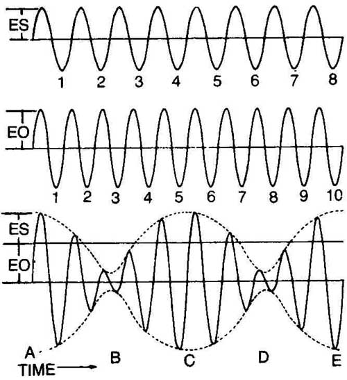
FIG. 16. Simplified graphical analysis of the formation of beats.
In this example, one voltage, es, has a frequency of 8 cycles per second and the other voltage, eo, has a frequency of 10 cycles per second. Initially, the amplitudes of the two voltages add at instant A but at instant B the relative phase of eo has advanced enough to oppose es, and the amplitude of the resultant envelope is reduced to a value dependent upon es. At instant C the relative phase of eo has advanced enough to permit the amplitudes to add again. Thus, one cycle of amplitude variation of the envelope takes place in the time interval that eo needs to gain one cycle over es. From FIG. 16 it may be seen that eo gains two cycles in the interval A to E. Therefore, the beat or difference frequency is 2 cycles per second. In the superheterodyne receiver the amplitude of the oscillator signal is designed to be greater than that of any received signal.
I-F Amplifier
The IF amplifier is a high-gain circuit commonly employing pentode tubes. This amplifier is tuned to the frequency difference between the local oscillator and the incoming RF signal. Pentode tubes are generally employed with one, two, or three stages, de pending on the amount of gain needed. As previously stated, all incoming signals are converted to the same frequency by the frequency converter, and the IF amplifier operates at only one frequency. The tuned circuits, therefore, are permanently adjusted for maximum gain consistent with the desired bandpass and frequency response. These stages operate as class-A voltage amplifiers, and practically all of the selectivity of the superheterodyne receiver is developed by them.
FIG. 17 shows the first IF amplifier stage. The minimum bias is established by means of R1 C1. Automatic volume control can be applied to the grid through the secondary of the preceding coupling transformer.
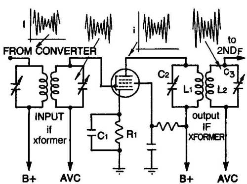
FIG. 17. First IF amplifier stage.
The output IF transformer, which couples the plate circuit of this stage to the grid circuit of the second IF stage, is tuned by means of capacitors C2 and C3. Mica or air-trimmer capacitors were used in old-time radios. In newer radios the capacitors are fixed, and the tuning is accomplished by means of a movable powdered-iron core. This method is called permeability tuning. In special cases only the secondary is tuned (single tuned). The coils and capacitors are mounted in small metal cans that serve as shields, and provision is made for adjusting the tuning without removing the shield.
The input IF transformer has a lower coefficient of coupling than he output transformer in some receivers in order to suppress noise from the pentagrid converter. The output IF transformer is slightly over-coupled with double humps appearing at the upper and lower sideband frequencies. The overall response of the stage is essentially flat, and in typical broadcast receivers has a voltage gain of about 200 with a bandpass of 7 to 10 kHz and an IF of about 456 kHz.
The chief characteristic of the double-tuned band-pass coupling is that at frequencies slightly above and slightly below the intermediate frequency, the impedance coupled into the primary by the presence of the secondary is reactive. This cancels some of the reactance existing in the primary, and the primary current increases. Thus the output voltage of the secondary does not fall off, and the response is uniform within the pass band.
Demodulation of Waves
Demodulation, or detection, is the process of recovering the intelligence from a modulated wave. When a radio carrier wave is amplitude-modulated, the intelligence is imposed on the carrier in the form of amplitude variations of the carrier. The demodulator of an amplitude-modulated (AM) wave produces currents or voltages that vary with the amplitude of the wave. Likewise, the frequency- modulation (FM) detector and the phase-modulation (PM) detector change the frequency variations of an FM wave—and the equivalent phase variations of a FM wave—into currents or voltages that vary in amplitude with the frequency or phase of the carrier.
The detector in the receiver must therefore be designed so that it will be sensitive to the type of modulation used at the transmitter, and generally insensitive to any other.
Most collectible radios are designed for amplitude modulation. A dear understanding of the mechanism of AM detection is there fore very important.
AM modulators and demodulators are nonlinear devices. A nonlinear device is one whose current to voltage relationship is not a straight line. Because the ratio of current to voltage is not constant, the device has a nonlinear impedance—for example, in one of the electron-tube detectors to be considered later, the average output current is the difference between each successive positive and negative swing of the output signal current, as shown in FIG. 18. The average output (signal component) follows the envelope of the incoming modulated wave more or less closely, depending on the shape of the nonlinear curve. Because the envelope of the incoming AM wave contains the desired audio frequency, a nonlinear device demodulates the AM wave.
For an understanding of the difference in the output frequencies of the various detectors, it is necessary to examine the frequencies involved in both modulation and demodulation.
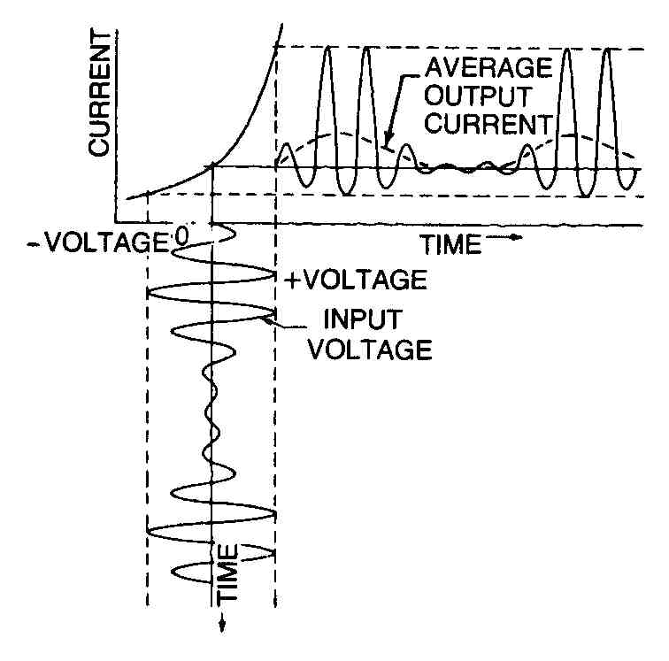
FIG. 18. Results of impressing an AM wave on a nonlinear device.
Comparison of Amplitude Modulation and Demodulation
If at the transmitter, an RF carrier and a single-frequency audio-modulating signal of sine waveform are impressed on a linear device, the output waveform from the linear device will contain the same RF and AF signal frequencies. The tuned RF amplifiers in the transmitter will amplify the RF carrier but will eliminate for all practical purposes the AF component. Under these circumstances, only the carrier will be radiated, and it will be ineffective in carrying the intelligence component.
A very different result is obtained if an RF carrier and a single- frequency audio-modulating signal of sine waveform are impressed on a nonlinear device. In this instance distortion is introduced and, as a result, additional frequencies are produced. In addition to the original frequencies, sum-and-difference frequencies are generated, and a zero-frequency, or DC component, is added. The tuned circuits at the transmitter now respond to the carrier and the upper and lower sidebands. As before, though, the AF modulating signal is discriminated against. However, this AF component is replaced, or generated, by the demodulator in the receiver.
In the receiver the carrier and the two sidebands are impressed on a second nonlinear device called the demodulator. If the demodulator has an ideal nonlinear curve, it will distort the incoming waveform (the positive halves of the cycle will be different from the negative halves). Therefore, in addition to the RF carrier and the two sidebands, the signal frequency—the difference between the upper sideband and the carrier or the difference between the carrier and the lower sideband—and a zero-frequency, or DC component will be produced. This DC component may be used for automatic volume control.
If the demodulator used in the receiver does not have an ideal nonlinear curve but has a practical realizable curve such as the square-law curve, additional frequencies will be produced. These frequencies will be harmonics of all frequencies present in the input. They are produced because input voltages having larger amplitudes are distorted differently from input voltages having smaller amplitudes. The RF harmonics may be filtered in the output of the demodulator, but the AF harmonics are not easily eliminated.
Thus, modulation and demodulation are essentially the same in that the waveform is distorted in each case and new frequencies are produced.
Types of AM Detectors
Detectors are classified according to the shape of their current-voltage (characteristic) curve. If the curve is smooth, as in FIG. 18, the detector is called a square-law detector. It is called a square-law detector because, for a first approximation, the output voltage is proportional to the square of the effective input voltage.
If the current voltage curve of the detector is shaped like an obtuse angle, as in FIG. 19A, the curve is still nonlinear because of the abrupt change in shape at the knee. Because the detector action takes place on the linear portions of the curve on both sides of the voltage applied to the plate on the next cycle exceeds the potential at which the capacitor holds the cathode (point B), diode current again flows and the capacitor charges up to almost the peak value of the second positive half cycle at point C.
So the voltage across the capacitor follows very nearly the peak value of the applied RF voltage and reproduces the AF modulation. The detector output, after rectification and filtering, is a DC voltage that varies at an audio rate, as shown by the solid line in FIG. 20E. The curve of the output voltage across the capacitor is shown somewhat jagged. Actually, the RF component of this voltage is negligible and, after amplification, the speech or music originating at the transmitter is faithfully reproduced.
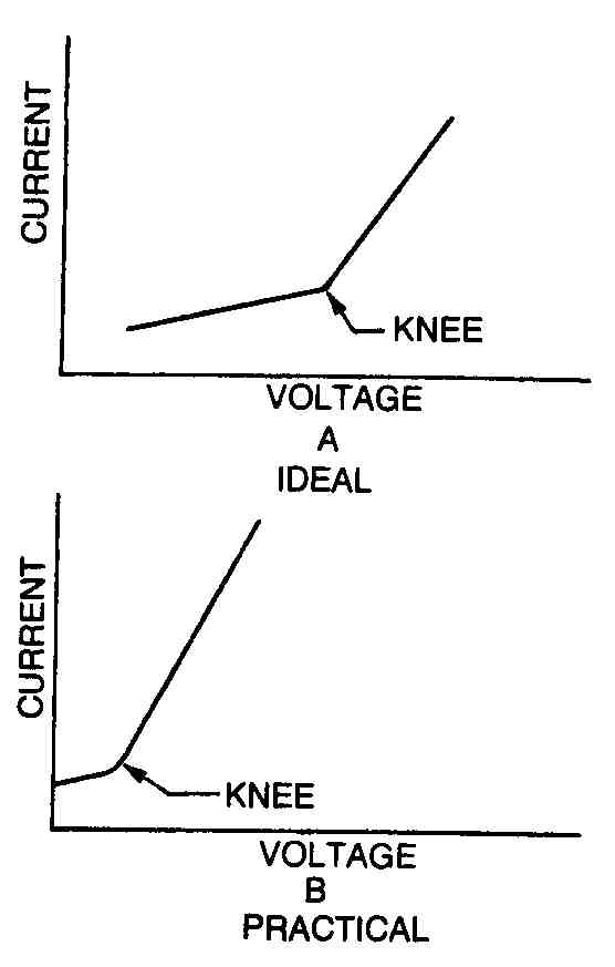
Fig. 19. Linear detectors.
The correct choice of R and C2 ( FIG. 20A) in the diode- detector circuit is very important if maximum sensitivity and fidelity are to be obtained. The load resistor, R, and the plate resistance of the diode act as a voltage divider to the received signal. Therefore, the load resistance should be high compared with the plate resistance of the diode so that maximum output voltage will be obtained. The value of C2 should be such that the RC time constant is long compared with the time of one RF cycle. This is necessary because the capacitor must maintain the voltage across the load resistor during the time when there is no plate current. Also, the RC time constant must be short compared with the time of one AF cycle in order that the capacitor voltage can follow the modulation envelope.
The values of R and C2 therefore place a limit on the highest modulation (audio) frequency that can be detected. FIG. 20F shows the type of distortion that occurs when the RC time constant is too large. At the higher modulation frequencies, the capacitor does not discharge as rapidly as required, and negative peak clipping of the audio signal results.
The efficiency of rectification in a diode is the ratio of the peak voltage appearing across the load to the peak input signal voltage. The efficiency increases with the size of R compared with the diode plate resistance, because R and the diode are in series across the input circuit and their voltages divide in proportion to their resistance. With audio frequencies, a large value of R may be used (of the order of 100,000 ohms), and consequently the efficiency is relatively high (95 percent). When high modulation frequencies are necessary, the value of R must be reduced to keep the RC time constant low enough to follow the envelope. Consequently, the efficiency is reduced.
The diode detector can handle large signals without overloading, and it can provide automatic volume control voltage without extra tubes or special circuits. However, it has the disadvantage of drawing power from the input tuned circuit because the diode and its load form a low-impedance shunt across the circuit.
Consequently, the circuit Q, the sensitivity and the selectivity are reduced. The interelectrode capacitance of the diode detector limits its usefulness at high carrier frequencies, and the bend in the lower portion of current-voltage characteristic indicates that it distorts on weak signals. Therefore, considerable amplification is needed before detection.
Grid-Leak Detector
The grid-leak-detector functions like a diode detector combined with a triode amplifier. It is convenient to consider detection and amplification as two separate functions. In FIG. 21A, the grid functions as the diode plate. The values of Cd and Rd must be so chosen that Cd charges during the positive peaks of the incoming signal and discharges during the negative peaks. The time constant of Rd Cd should be long with respect to the RF cycle and short with respect to the AF cycle.
An approximate analysis of the waveforms existing in the diode (grid) circuit is shown in FIG. 21B. Part 1 shows the input waveform, which is also the waveform in the input tuned circuit. Because RF current g flows in only one direction in the grid circuit, part 2 shows a rectified current waveform in this circuit. Part 3 shows the waveform developed across Cd. This audio waveform is produced in the same way as the audio waveform in the diode detector. However, the waveform shown in part 3 is not the output voltage. In the grid-leak detector, the waveform produced across Cd is combined in series with the RF waveform in the tuned circuit to produce the grid-to-cathode waveform shown in part 4.
An approximate analysis of the waveforms existing in the triode plate circuit is shown in FIG. 21C. Part 5 is the plate-current waveform, and part 6 is the plate-voltage waveform.
Capacitor C discharges on the positive half cycles of grid input voltage (points 1, 3, 5, 7, 9, 11, 13 and so forth). The discharge path is clockwise through the circuit including the tube and capacitor. The time constant of the discharge path is the product of the effective tube resistance and the capacitance of capacitor C. This time constant is short because the effective tube resistance is low. The increase in plate current is supplied by the capacitor rather than the B + supply, thus preventing any further increase in current through the RF choke and plate load resistor RL. Therefore, any further change in plate and capacitor voltage is limited.
Capacitor C charges up as plate voltage rises on the negative half cycles of RF grid input voltage ( FIG. 21C, points 2, 4, 6, 8, 10, 12, 14 and so forth). The charging path is clockwise through the circuit containing the capacitor, RF choke, load resistor RL and the B+ supply. The rise in plate voltage is limited by the capacitor charging current that flows through the RF choke and through RL. The plate current decrease is approximately equal to the capacitor charging current so the total current through the RF choke and R_L remains nearly constant, and the plate and capacitor voltage rise is checked.
Positive grid swings cause sufficient grid current flow to produce grid-leak bias. Low plate limits the plate current on no signal in the absence of grid bias. Accordingly, the amplitude of the input signal is limited, since with low plate voltage the cutoff bias is low, and that portion of the input signal that drives the grid voltage below cutoff is lost. The waveform of the voltage across capacitor C is shown by the solid line in part 6 of FIG. 21C. The plate voltage ripple is removed by the RF choke (RFC). Part 7 shows the output- voltage waveform. This waveform is the difference between the voltage at the junction of R and RFC with respect to the negative terminal of Eb and the voltage across coupling capacitor Cc, which for most practical purposes is a pure DC voltage.
Because the operation of the grid-leak detector depends on a certain amount of grid-current flow, a loading effect is produced which lowers the selectivity of the input circuit. However, the sensitivity of the grid-leak detector is moderately high on low- amplitude signals.
Plate Detector
In a grid-leak-detector the incoming RF signal is detected in the grid circuit and the resultant AF signal is amplified in the plate circuit. In a plate detector, the RF signal is first amplified in the plate circuit, and then it is detected in the same circuit.
A plate detector circuit is shown in FIG. 22A. The cathode bias resistor, R1, is chosen so that the grid bias is approximately at cutoff during the time that an input signal of proper strength is applied. Plate current then flows only on the positive swings of grid voltage, during which time average plate current increases. The peak value of the AC input signal is limited to slightly less that the cutoff bias to prevent driving the grid voltage positive on the positive half cycles of the input signal. As a result, no grid current flows at any time in the input cycle, and the detector does not load the input tuned circuit, LC1.
Cathode bypass capacitor C2 is large enough to hold the voltage across R1 steady at the lowest audio frequency to be detected in the plate circuit. C3 is the demodulation capacitor across which the AF component is developed. R2 is the plate load resistor. The RF choke blocks the RF component from the output. R2R3 has a long time constant with respect to the time for one RF cycle so that C3 resists any voltage which occurs at the RF rate. R2C3 has a short time constant with respect to the time for one cycle so that the capacitor is capable of charging and discharging at the audio rate.
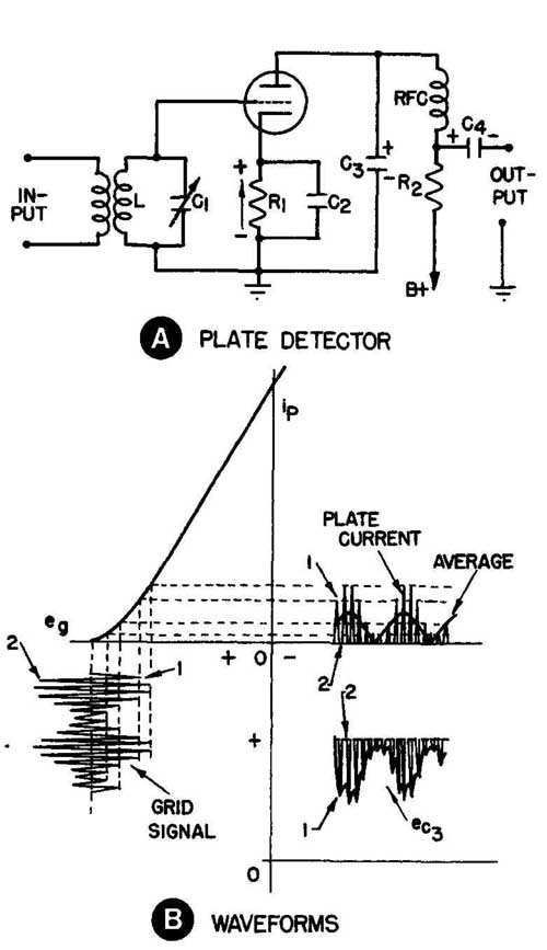
FIG. 22. Plate detector and waveforms.
The action of the plate detector may be demonstrated by the use of the ip-eg_curve in FIG. 22B. On the positive half cycle of RF input signal (point 1), the plate voltage falls below the B+ supply because of the increased drop across R2and the r f choke. Capacitor C3 discharges. The discharge current flows clockwise through the circuit including the tube and C rather than the B supply. The drop across R2 and the RF choke is limited, and the decrease in plate voltage is slight.
On the negative half cycle of RF input signal (point 2) plate current is cut off and plate voltage rises. Capacitor C3 charges. The charging current flows clockwise around the circuit, including the RF choke, R2 and the B + supply. The drop across R2 and the RF choke contributed by the charging current of C3 checks the rise in plate voltage.
Thus, C3 resists voltage change at the RF rate. Because C3R2 has a short time constant with respect to the lowest AF signal, the voltage across C3 varies at the AF rate.
The plate detector has excellent selectivity. Its sensitivity (ratio of AF output to RF input) is also greater than that of the diode detector. However, it is inferior to the diode detector in that it is unable to handle strong signals without overloading. Another disadvantage is that the operating bias will vary with the strength of the incoming signal and thus cause distortion unless a means is provided to maintain the signal input at a constant level. This is why AVC or manual RF gain control circuits usually precede the detector.
Second Detector
Most superheterodyne receivers employ a diode as the second detector. This type of detector is practical because of the high gain as well as the high selectivity of the IF stages. The diode detector has good linearity and can handle large signals without overloading. For reasons of space and economy, the diode detector and first audio amplifier are often included in the same envelope in modern superheterodyne receivers.
A simple diode detector is shown in FIG. 23. The rectified voltage appears across R1, which also serves as the volume control potentiometer. Capacitor C2 bypasses the RF component to ground, and C3 couples the output of the detector to the first audio amplifier stage. The tuned circuit, L2C1 is long compared to the time for one IF cycle but short compared to the time for one AF cycle, if the intermediate frequency is 456 kHz, the time for one IF cycle in microseconds is
1/0456 =2.19 us
If R1 is 250K and C2 is 100 pF, the time constant in microseconds is 0.25 x 100 = 25 ps
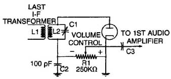
FIG. 23. Diode detector.
The demodulation capacitor, C2, discharges through R1 in one-half the time for one AF cycle, 1/2f. The time required to discharge C2, is 5R1C2 seconds. Thus
1/2f = 5R/f
= 1/10 xR1x C2
=1/10 x 0.250 x 106 x 100 x 10_12
= 103/0.250
= 4000Hz
So the highest audio frequency that C2 is capable of following without distortion is, in this example, 4000 Hz. In order to increase the response of the diode detector, the time constant of R1C2 is reduced, for example, by decreasing R1 to 100K. The highest audio frequency now becomes
f= 1/10xR1xC2
= 1/10
= 10000Hz
Demodulation capacitor C2 cannot discharge rapidly enough to follow modulation frequencies higher than 10,000 Hz (in this case), and clipping results with all higher audio frequencies.

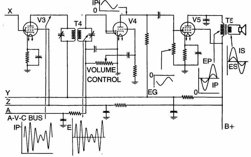
FIG. 24. Circuit diagram of a superheterodyne receiver.
Circuit of a Superheterodyne Receiver
The complete circuit of a superheterodyne receiver is shown in FIG. 24. In this circuit one RF amplifier (preselector) stage is used. Tube V2, a pentagrid converter, serves both as the mixer tube and oscillator tube. Three tuning capacitors (one each in the preselector, mixer and oscillator stages) are ganged on a common shaft to assure proper tracking. Trimmers are connected in parallel with each capacitor to permit alignment. The oscillator tuning capacitor is smaller than the tuning capacitor in the preselector or the converter stages. The oscillator operates above the station frequency and tracks closely at three points on the dial—the low end, the middle and the high end. The oscillator tuning capacitor split-rotor plates allow closer adjustment for tracking at the low end and at the middle of the band. Shunt trimmer capacity adjustments on the oscillator tuning capacitor provide close tracking of the oscillator at the high end of the band.
Tube V3 is the IF amplifier with input and output IF transformers tuned to the receiver intermediate frequency.
Tube V4 serves as the second detector and first audio amplifier. Conventional automatic volume control is tapped off at the end of the volume control potentiometer farthest from ground. Plate and screen potentials are obtained from the B+ supply through the cones ponding voltage-dropping resistors. The power supply is a conventional full-wave rectifier.
The final stage in the receiver contains a power amplifier; it may be single ended or push-pull. FIG. 24 shows a complete power amplifier stage containing V5, associated resistors and capacitors, a transformer and a speaker. The stage operates as a class A amplifier in this case, since it is single ended. If push-pull is used, the stage can operate as class A, AB or B. In any case, the energy is transformer- coupled to the load—the speaker in FIG. 24—for better impedance matching.