For constant reference while working on repairs, the TV technician’s constant companion should be a schematic diagram. Certainly the schematic diagram is one of the most important tools of anyone who works with electronic or electrical equipment. If you expect to do any TV repair work, or have anything to do with handling electrical or electronic equipment, you need a working knowledge of these diagrams. This guide was created with the assumption that you already have some experience in reading schematics; but this appendix is included to give some pointers on the specifics of television schematics.
Schematic Diagram Basics
Schematic diagrams are designed to provide a graphic presentation and analysis of electrical equipment components, and how they are connected. However, the schematic diagram is not an explanation of the function. Rather, the technician must be able to interpret the diagram. The schematic diagram should not be confused with other types of diagrams, such as block diagrams, wiring diagrams or layout diagrams. Because schematic diagrams show only basic electrical circuit functions, and not physical characteristics, a diagram often will be exactly the same for circuits that appear to be different. Conductors and components in a schematic diagram are arranged in such a way that they do not resemble their actual physical arrangement. Arranging everything in a schematic diagram to conform with the actual features of an electronic component could make it hard for the technician to interpret the circuit function of the components, which is, after all, the primary purpose of the schematic diagram.
Component names and connections are apparent to anyone who examines the equipment. Understanding how a component functions requires knowledge of the circuits being used. This is where the schematic diagram is the most useful: when the technician is troubleshooting, repairing, and operating the electronic components.
Here are a couple of basic tips on reading general schematic diagrams, if you aren’t familiar with using them. First of all, straight lines represent all connecting conductors, despite the type of conductor being used, whether a huge bus bar or a tiny wire. Several different types of conductors could be used in the component in question, but in the schematic diagram they will all be depicted as simple straight lines. Occasionally, a heavier line is used to depict a heavy ground bus or a metal chassis; but for the most part, all conductor lines are thin, regular lines.
If some conductors within a given circuit connect, a dot is placed at the point where the conductor lines cross, or where one conductor line ends as it reaches another. If conductor lines cross but do not connect, there is no dot; sometimes a “jumper” is drawn to show that one conductor jumps over the other instead of connecting to it.
The Television Schematic
The schematic diagram of a typical television receiver is rather complex. The television sound system is identical to that of FM radio, while the picture system is more like an AM system; except, of course, that pictures rather than sound are broadcast.
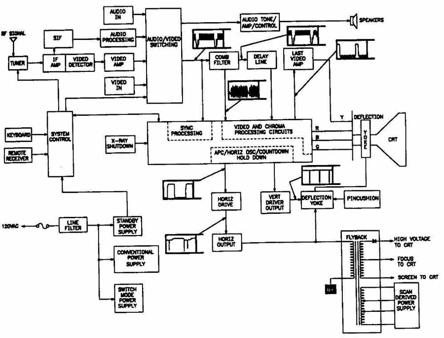
FIG. 1. Block diagram of a color television receive, showing the black-and-white
stages.
The schematic diagram for a typical television receiver is rather large and complex, so we shall first examine the overall block diagram before looking at specific components within the schematic diagram. (See FIG. 1.)
The Receiver Block Diagram
The location of any circuit within the actual television set is important in interpreting the overall schematic diagram. For this reason, we will first review the TV circuits.
Color television, of course, dominates the TV broadcast industry, but many black-and-white sets are still in use. The only difference between a color receiver block diagram and one for a black-and-white set is that a separate sound detector isn’t used in the black-and-white set. The video detector is used for both functions, and the sound IF signal moves from the video detector to the sound IF amplifier.
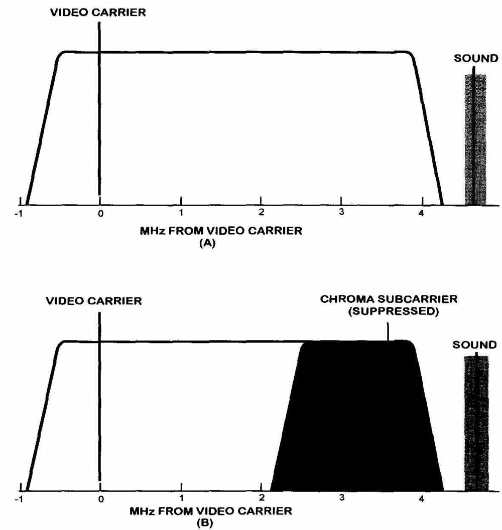
FIG. 2. Black-and-white (A) and color (B) television signals.
The antenna signal enters through the tuner or front end, the section that contains the oscillator, the mixer and the RF amplifier. Included in the signal are the frequencies of the black-and-white and color signals ( FIG. 2). Please note that there are two separate carriers, one each for sound and picture. In addition, the bandwidth of the signal is almost 6 MHz: the frequency space set aside for each television channel. This bandwidth also includes the sound and picture side bands. Back in FIG. 1, the frequency components are contained in the tuner and video IF amplifier sections, after which the amplified signals are split into the sound and video detectors.
The mixer output contains the video IF and sound IF signals; the sound signal is 4.5 MHz lower than the video signal’s frequency. Both the sound and video IF signals are amplified by the video IF amplifier, which also applies them to the video and sound detectors. These signals mix (hetero dyne) in the sound detector to produce a third signal with a carrier frequency of 4.5 MHz (the difference between the carrier frequencies of the two IF signals). The carrier is frequency modulated by the audio signal and, to an extent, amplitude modulated by the video signal. The limiting action of the amplifier stage removes the amplitude modulation. The 4.5 MHz sound IF signal is amplified in the sound IF amplifier, and demodulated in the sound demodulator, creating an AF signal. The AF signal is then amplified in the AF amplifier and sent to the loudspeaker. At least one IC is used in the sound section of most receivers.
The video IF amplifier output goes through the video detector, where the video elements of the signal are separated. The video elements consist of information for a black-and-white picture (luminance), color (chrominance) and synchronization between picture and color (sync).
In FIG. 1, you can see the destinations of the signals used for black-and-white reception. The video signal moves from the video amplifier to the grid of the picture tube. The sync elements move to the sync section, where they are used to control the vertical and horizontal sweep oscillators. The sync elements also supply pulses for the high-voltage power supply and occasionally part of the low-voltage supply.
The other color sections are shown in FIG. 3. You can see that the luminance pail of the signal encounters a delay line in its path. The delay line holds the luminance signal just long enough to allow the other color signals to “catch up” in their respective sections; therefore, all color signals reach the picture tube at the same moment.
In the meantime, the chrominance elements leave the video amplifier to be filtered and amplified in the chroma bandpass amplifier. From there, they move through the chrominance demodulator, then to the picture tube. The two chrominance signals, R-Y and B-Y, are separated by the demodulation process and then combined to produce the G-Y signal. The red (R-Y), blue (B-Y) and green (G-Y) signals (known as color or difference signals) are then applied to the picture tube, or matrixed to produce red (R), green (G) and blue (B).
The color burst and sync signals, derived from chrominance information, are used to put the color video elements in sync, by synchronizing the subcarriers in the chrominance demodulator. These signals move from the chroma amplifier to the burst amplifier, which separates them. The color killer switches off the chrominance amplifier if there are no color signals.
As shown in FIG. 4, the tuner stage selects one channel from all of the signals received by the antenna. Each channel consists of an RF frequency containing two carriers: the FM sound carrier and the AM video carrier. The tuner circuit adjusts the lever of the RF signal and converts it into an IF signal. So, the tuner circuit has one input, the RF frequency, and one output, the IF signal, though there are two carriers in the RF frequency. See Section 9 for tips on troubleshooting tuners.
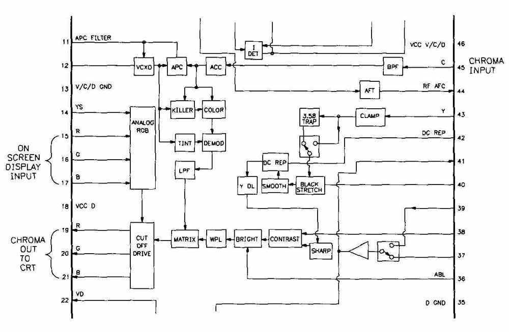
FIG. 3. A color TV color sections.
The Tuner Stage
Each of the television stations in a geographic area transmits on a specific frequency. To select one signal and have all of the other stages in the chassis recognize the selected signal without having to constantly retune, televisions use a tuning method called heterodyning.
In heterodyning, when you select a channel, the RF amplifier is tuned to that frequency. The RF amplifier amplifies the signal and outputs it to the mixer stage. Then, the oscillator outputs its signal reference to the mixer. These two input signals are mixed so that the output signal from the mixer is the difference between the two signals, or the intermediate frequency (IF). All of the later stages in the chassis are permanently tuned to the IF so that they do not have to be retuned each time you select a new channel.
There are two types of tuner circuits. A “discrete” tuner is composed of individual components that are part of the main board. If a discrete tuner is not working correctly, you can test the components, locate the one that is faulty, and repair it. A “modular” tuner is a replaceable unit that is easier to replace than try to repair when it is faulty. FIG. 5 shows a block diagram for a “generic” tuner circuit.
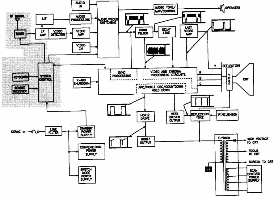
FIG. 4. The tuner stage (shaded).
Manufacturers have developed several types of tuners, including varactor (variable capacitance diode) and frequency synthesis tuners. However, all tuners, including the older mechanical tuners and hybrid tuners, have three main tuner stages: RF amplifier, oscillator and mixer.
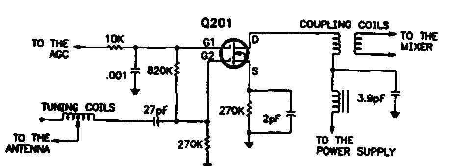
The RF amplifier provides frequency selectivity, improves the signal-to-noise ratio, and prevents the radiation from the oscillator from leaking back to the antenna. The RF amplifier stage, shown in FIG. 6, selects one RF signal from all of the signals being received by the antenna, amplifies it, and outputs it to the mixer. The AGC (automatic gain control) is connected to the RF amplifier and controls the gain of the amplifier by offsetting variations in the carrier signals. The RF amplifier can be a transistor or a FET (field effect transistor).
The television’s antenna is part of the RF amplifier circuit. The RF amplifier blocks the signal from the oscillator from leaking back to the antenna. Signal leaking can cause picture interference.
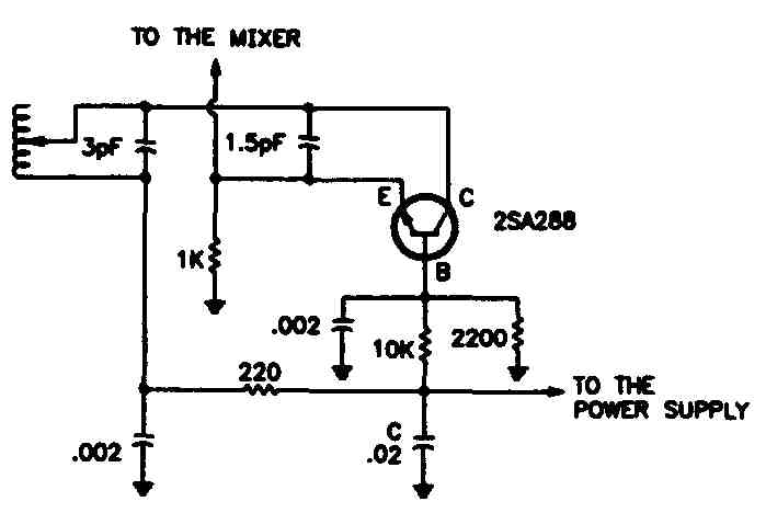
The oscillator stage, like the one shown in FIG. 7, outputs an unmodulated reference signal to the mixer that tracks the desired RF signal at a fixed, offset frequency. The frequency of the signal is manufacturer dependent.
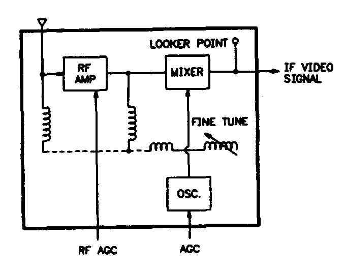
FIG. 5. A generic tuner circuit.
Also, tuners have an AFT (automatic fine tuning) circuit connected to the oscillator. The AFT shifts the oscillator frequency as needed to keep the signal in phase with the selected channel frequency. Older televisions have manual fine tuning controls that keep the signal in phase with the channel frequency.
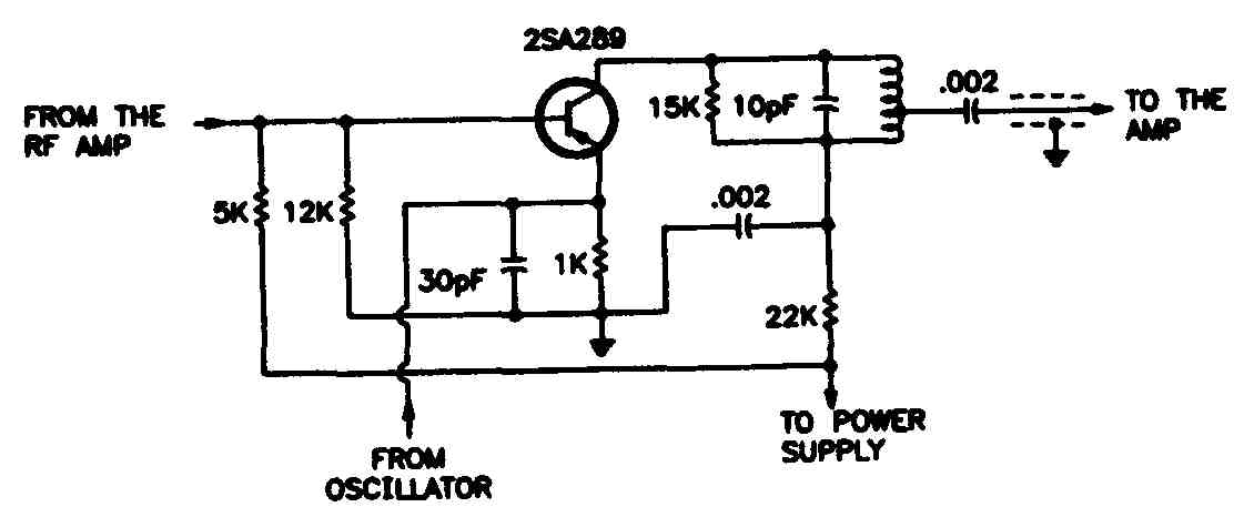
The mixer stage, like the one in FIG. 8, inputs the RF and oscillator signals, mixes them, strips out the extraneous signals from the original RF and oscillator signals, and produces the IF signal. The conversion must be performed without distorting the incoming signal. Mixers are sometimes called frequency converters, frequency translators or heterodyne detectors.
The output from the mixer is an IF signal, as shown in FIG. 9. The frequencies represented in the signal are constant so that the signal can be used in later stages in the chassis:
39.75 MHz — The adjacent channel’s video carrier.
41.25 MHz — Audio carrier.
41.67 to 42.69 MHz Color carrier.
45.75 MHz — Video carrier.
47.25 MHz — Adjacent channel’s audio carrier.
Listed here are only three of the types of tuners you will see. The design of most tuners is dependent on the individual manufacturers. A varactor tuner is a diode that acts like a variable capacitor when the diode is biased by a variable voltage supply. The capacitance can be changed over a large range of frequencies by inputting a control voltage from the regulated low-voltage power supply. When a channel is selected, a pre-selected voltage for that channel is applied to the diode. This causes the diode to align with the selected frequency. When you fine-tune the frequency, the applied voltage is adjusted using an AFT correction voltage until the diode is completely aligned with the frequency.
A reactance tuner consists of coils and a capacitor. Each coil is assigned to a tuner frequency. The coils are connected with a multiple contact switch or a series of diodes used as switches. When a new channel is selected, the switch contacts another coil, and the channel changes.
A frequency synthesis (FS) tuner, also known as digital tuning or quartz tuning, provides up to 127 channels and all of the UHF frequency band. The ES circuit is an IC that contains additional stages such as a phase-lock loop (PLL), step generator, a frequency band switch decoder, an AFT, digital sync, and a presence decoder. Refer to the schematic for details about the FS tuner.
Phase-Locked Loop (PLL) Synthesizer System
The phase-locked loop (PLL) is a system through which a frequency signal can be frequency stabilized through the control of a standard reference oscillator. The operation of a PLL system is depicted in FIG. 1O.
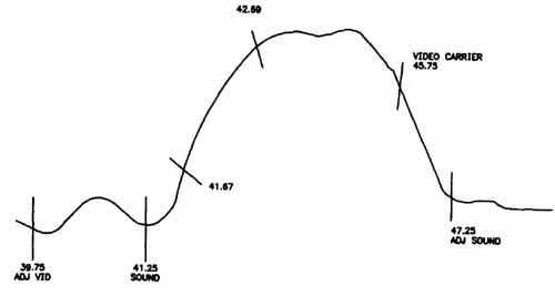
FIG. 9. An IF signal waveform.
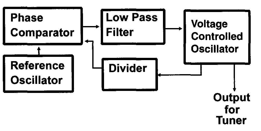
FIG. 10. A phase-locked loop (PLL) synthesizer system.
The varactor in the voltage-controlled oscillator (VCO) circuit varies the oscillator frequency according to a DC voltage being applied to the varactor. Usually, the reference oscillator is a fixed-frequency, crystal-controlled circuit. In FIG. 10, the reference oscillator frequency is relatively low, so its stability is ensured. VCO and reference oscillator outputs are applied to a phase comparator. The VCO signal is passed through a divider that reduces its frequency so it comes close to matching the reference oscillator in value (the VCO frequency is higher than that of the reference oscillator).
The VCO and reference signal phases and frequencies are compared in the comparator. If the signals are different in any way, a DC (or difference) voltage develops. The difference voltage moves back into the VCO to correct the oscillator frequency, so that it matches that of the reference signal.
In FIG. 10, the reference setting fixes the received oscillator frequency and channel, since programmed dividers can operate at any integral multiple of the oscillator frequency.
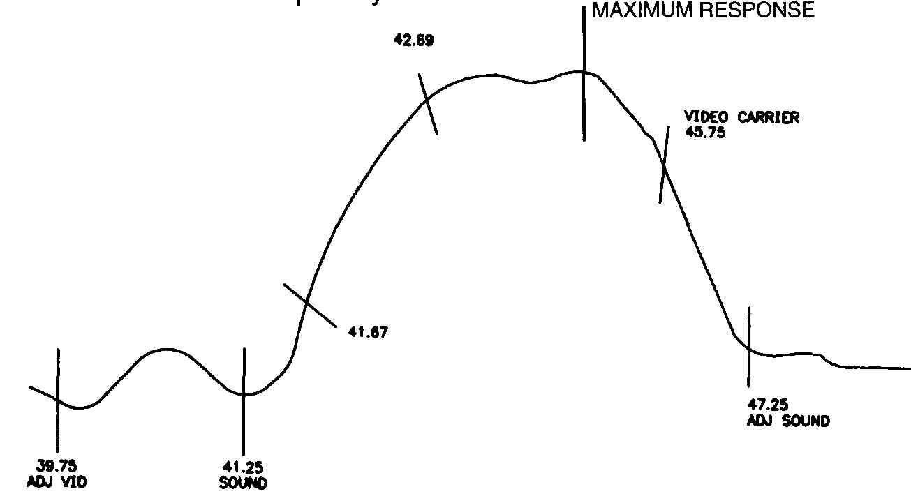
FIG. 11. An IF signal waveform with maximum response curve indicated.
Video
IF amplifiers used for television video are similar to those used in radios. The television IF is designed to amplify a wide band of frequencies (almost 6 MHz) to include the carriers and side bands shown in FIG. 2. The video IF amplifier must have a frequency response that maintains the ratio of the video and sound IF amplitudes (see FIG. 11).
Most television receivers use ICs in the IF amplifier, so ICs are indicated in the amplifier section in a schematic diagram. FIG. 12 shows a typical IF section. Note that one IC (shown in three parts, IC1A, IC1B and IC1C) is used for the IF and detector sections. The tuned circuits are external to them, and the IC contains the active components, such as the transistors. IF alignment is accomplished through the IF transformers, which is why they are kept physically accessible. FIG. 12 also shows the video detector and the first video amplifier circuit.
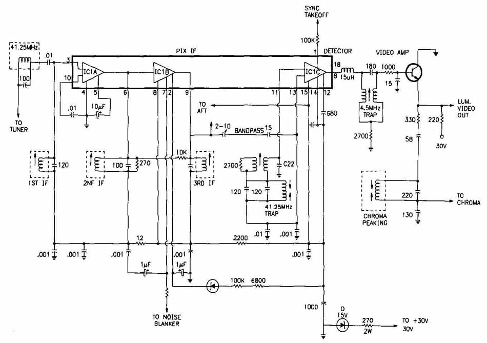
FIG. 12. An IF amplifier section, connected to an AGC.
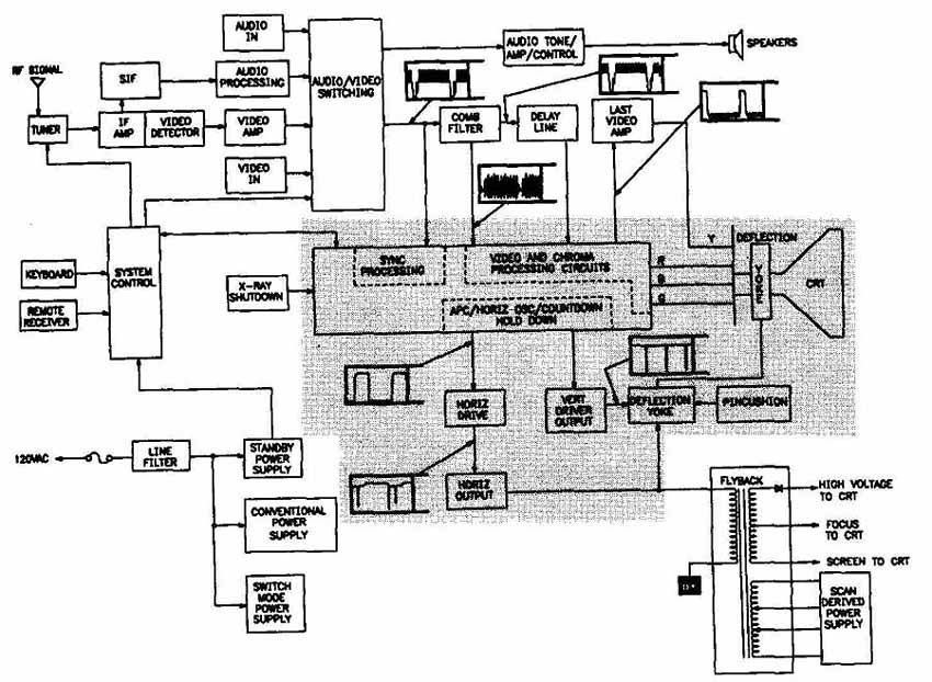
FIG. 13. The television picture sync and deflector circuits (shaded).
The coupling transformer between IC3 and the video amplifier acts as a trap to eliminate the 4.5 MHz sound IF signal from the video and sync composite signals. The sound IF signal is from the output of IC2, as indicated in FIG. 12. There is a separate detector for sound in color TV receivers. The sound detector separates the sound IF signal from the video IF signal. The resulting signal is a mix of the high-frequency sound IF (41.25 MHz) and video IF signals (45.75 MHz). Its frequency is the difference between them.
When the video signal is retrieved from the IF signal, it is put through several stages (at least two) of amplification. The video amplifier supplies signals to three other receiver sections, consisting of the picture tube (through matrices), the chrominance amplifier and the picture sync section. The luminance or Y signal goes to the picture tube. The Y signal contains all the signal components for monochrome or black-and-white video. The luminance signal moves through the picture tube matrixing circuit, where it is mixed with chrominance to produce picture tube grid and cathode signals.
Sync and Deflection
Sync pulses in the video signal are used to keep the vertical and horizontal deflection signals in sync with the received signal. Sync pulses are divided into vertical and horizontal pulses, separate from the video signal. Sync circuits compare sample pulses from the receiver’s deflection circuits with the received pulses, and synchronize the frequency and phase of the received picture.
FIG. 13 shows a block diagram of the picture sync and deflection circuits. The separated vertical sync pulses move directly to the vertical deflection section, where they control the vertical oscillator frequency. When applied to the automatic frequency control (AFC) circuit, the horizontal sync pulses are compared to the pulses from the horizontal deflection circuit. Differences between the two results in a correction voltage being fed from the AFC circuit to the oscillator. The deflection signal sample used for comparison in the AFC is usually taken from the horizontal deflection section output stage.
FIG. 14 shows a vertical deflection circuit. The sync pulses trigger each cycle and keep the sweep in sync with the picture, when applied to the oscillator base circuit. The oscillator feeds a vertical pulse to the vertical output IC. The IC processes and compares the vertical signals in order to maintain a proper vertical output. The output moves to the vertical deflection yoke windings to ‘sweep’ the picture tube beam.
FIG. 15 shows a horizontal deflection circuit. Here the oscillator is synchronized by a DC voltage from the AFC circuit. This voltage corrects deviations of the oscillator frequency and phase. In the output stage, a power type transistor is used, which produces horizontal blanking to cut off the picture tube beam during retrace, current for pincushion magnets, heater current for the picture tube and pulses for the high-voltage power supply. The transistor can also be a source for a low-voltage power supply.
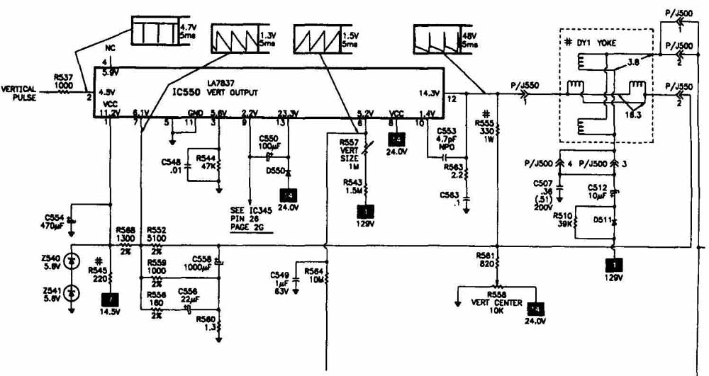
FIG. 14. Vertical deflection circuit.

FIG. 15. Horizontal deflection circuit.
Sound
FIG. 16 shows a block diagram of a sound section. In the video IF signal, the sound and video carriers are 4.5 MHz apart. The IF signal, which contains both signals, is fed to a separate detector in which the two signals are mixed, or heterodyned. The resulting difference heterodyne, based at 4.5 MHz, is used as the sound IF signal. To keep the FM sound modulation dominant in the 4.5 MHz sound IF signal, the high-frequency sound IF signal is maintained at a lower level than the video IF signal. Then, the 4.5 MHz IF signal is amplified and moved to the FM demodulator. The AF signal that results is then amplified in a regular amplifier.
The AF section is either all or partly included in an IC in nearly all television receivers. FIG. 16 shows an AF division into two ICs. FIG. 17, on the other hand, shows a circuit in which all AF components and the sound IF amplifier are included in one IC. The three main functions accomplished in the signal IC are illustrated in FIG. 17(A) and (B). Only the sound IF amplifier and demodulator are included in the IC in FIG. 18. Discrete components are used in the AF stages that follow.
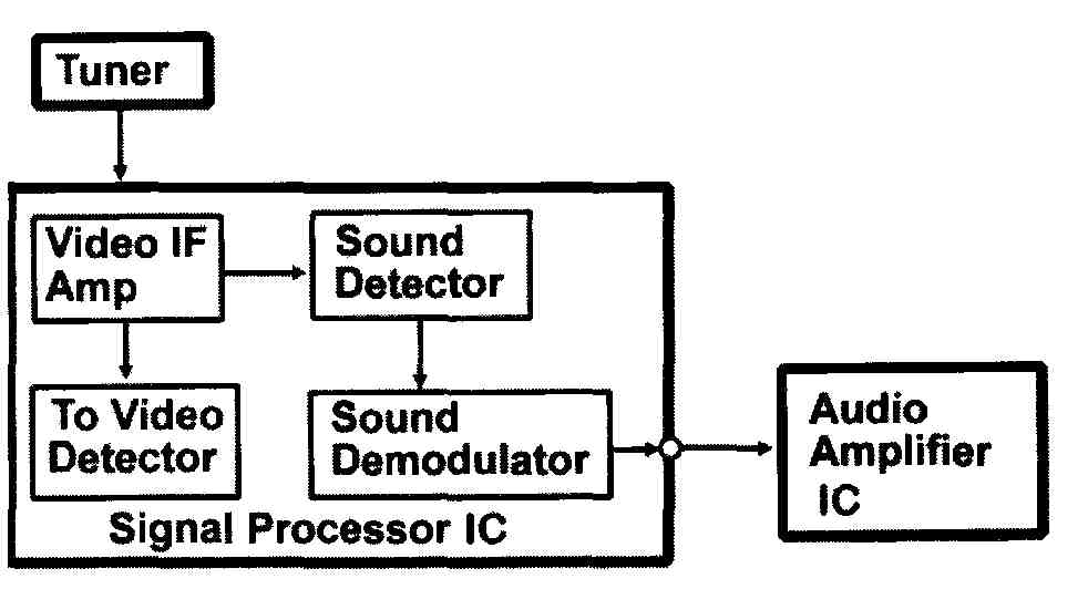
FIG. 16. Television sound system.
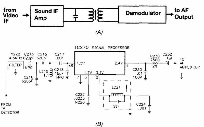
FIG. 17. An IC sound section showing (A) major portions of the IC, and (B)
an example circuit using ICs.
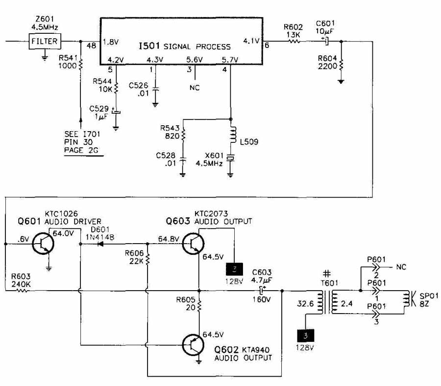
FIG. 18. In this sound section, only the sound IF amplifier and demodulator
are included in the IC.
Power Supplies
Low-voltage and high-voltage are the two power supplies used in a TV receiver. Low-voltage supplies provide current to the screen grids of the picture tube, to transistors, and to other devices requiring voltage in the 5- to 200-V range. The high-voltage power supply, 20 to 30 kV, is used for the anode and for the focus anode of the picture tube, 5 to 15 kV. All high- voltage (HV) supplies, and a few low-voltage ( LV) supplies, get their input from the horizontal output stage. Filtering is much simpler than with 60 Hz supplies because this current is at a frequency of 15,734 Hz. Some kind of 60 Hz supply must always be used, however, because current is needed to provide energy for the 15 kHz supplies, to operate the horizontal deflection section.
FIG. 19 shows the configuration of the 60 Hz LV power supply. In this example, a bridge rectifier supplies a 130 V regulator. These voltages are used to provide the necessary power for the horizontal deflection circuit. FIG. 20 shows the other type of LV supply, operating from the horizontal output circuit. In this case, the AC voltages are taken from the transformer at the output of the horizontal output transformer. Note that a Zener diode regulator is used for the 12 V output.
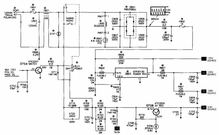
FIG. 19. The use of a 60 Hz low-voltage power supply.
High-voltage power supplies get their power from the horizontal output stage. A winding on the horizontal output transformer, or an extension of another, provides high-voltage pulses that are rectified or passed into a voltage multiplier. This in turn steps up the voltage while rectifying the signal. A typical high-voltage power supply circuit is shown in FIG. 21. Focus and screen voltages, needed for the picture tube, are also obtained from this supply.
Chroma Amplifier
The chroma, or chrominance amplifier (also called a bandpass amplifier) receives the signal from the video amplifier. This amplifier separates the chrominance side bands from the rest of the video signal. FIG. 2shows the frequency arrangement of the side band signals. The chroma side bands are part of the video signal, forming a modulated signal that must be de modulated in order to receive the chroma signals.
In FIG. 2(B), note that the chroma side bands are in the upper part of the video IF spectrum, from 3 MHz and up. So these side bands are de modulated and used properly, they are separated from the luminance video (Y signal) occupying the range under 3 MHz. The chroma amplifiers job is to handle this separation. The amplifier circuit itself is not much different from the video amplifier, but its constants limit response to the 1 MHz between 3 and 4 MHz.
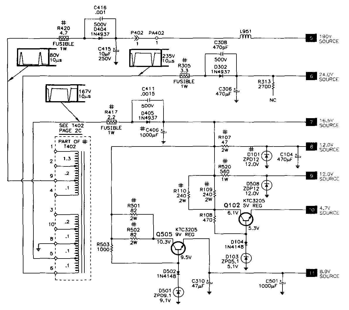
FIG. 20. Here the power supply receives input from horizontal deflection.
Color Sync
Demodulating the chrominance side bands requires the use of subcarriers to produce color signals that can be used at the picture tube. The subcarrier signal phases must be in sync in relation to a burst signal along each horizontal pulse. The color sync portion of the television receiver separates the color burst signals from the video signal, creates its own subcarrier signal and attaches it to the burst signal, and applies the resulting signal to the demodulator.
When the original signal is produced in the television studio, the camera captures the color and sends the signal to a modulator. The modulator circuit combines the three color signals into one color signal. This circuit also produces a color sync signal. The color signal is then called a color modulated signal. The color sync (color burst) signal is an unmodulated 3.58 MHz carrier. See Section 5 for more details.
A television’s color processing circuits recreate a color picture and produce the color picture on the screen. Essentially any color can be created from the primary colors red, green and blue (color difference signals R-Y, G-Y and B-Y).
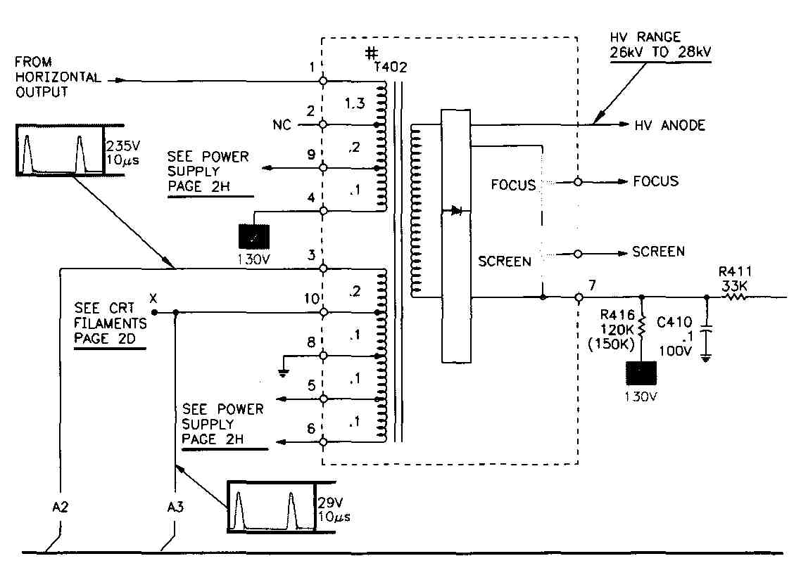
FIG. 21 . A high-voltage power supply circuit.
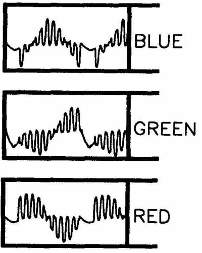
FIG. 22. Red (R), green (G) and blue (B) waveforms.
When the signal is received, the color sync signal turns on the 3.58 MHz oscillator and synchronizes it with the signal received from the station. The signal from the oscillator is output to the color killer, which turns on the color IF amplifiers so that the signal can be amplified. After amplification, the signal is passed to the color demodulator circuits. In the demodulator circuits the original red, green and blue signals (RY, G-Y and B-Y) are separated and sent to the red, green and blue color amplifiers. The color amplifiers combine the three color signals with the black-and-white luminance information, then pass the signals on to the three electron guns which pro- duce the color picture on the screen.
When these circuits malfunction, the result can be no color, color that is too intense, loss of one color, one or all wrong colors, or loss of color synchronization. For example, if the demodulator circuits fail, you might see no color, an incorrect tint or intensity, or intermittent color, tint or intensity. FIG. 22 shows the red, green and blue color waveforms to expect when testing the color circuits. (The waveforms are of a color bar pattern.)
Automatic kine bias (AKB) is circuitry used to adjust the beam current of each electron gun individually. This circuitry is intended to prolong the life of the electron guns and give optimum color setup. The setup is done only once in the lifetime of the CRT, or until a malfunction occurs within this circuit. The AKB IC samples the vertical blanking pulse for timing, and sources a small bias current to the cathode drivers to draw beam current individually on the electron guns. The AKB IC senses and adjusts with every vertical blanking pulse. For an optimum color screen setup, this is critical but relatively easy to set for most standard chassis.
Picture Tube Application
The color (difference) and Y signals must be combined and fed to the picture tube when they become available. Most picture tubes have three grids, each with a corresponding cathode, for the red, green and blue signals. The color signals are combined with the Y signal to cancel out Y and release R, G and B.
FIG. 23. Three methods for applying color signals to a picture tube. (A) shows the color circuits matrixed before the tube, (B) shows the color circuits at the grids, with the V signal at the cathode, and (C) shows the color signals being applied by the demodulator to the cathodes.
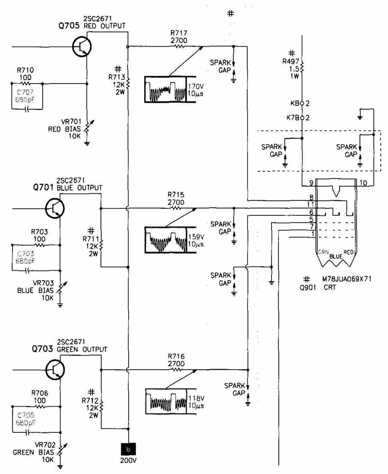
FIG. 24. Color amplifier circuit, showing brightness control and color drive
controls.
FIG. 23 shows some arrangements for combining or applying color signals to the picture tube. The three color signals are combined in matrices with the Y signal to derive R, B and G, as shown in FIG. 23(A). These signals are then applied to their respective grids. The DC-biased cathodes are grounded to the signals, and the color signals are applied to the grids, as shown in FIG. 23(B). A -Y signal is applied to the cathodes, which causes the Y signal to add to the color-difference signals. As a result, one of the three signals, red, green and blue, is applied between the grid and the cathode of each gun in the tube. Figure G-23(C) shows that the color signals are applied to the cathodes, and the grids are at signal ground; the opposite of what is shown in (A).
FIG. 24 shows a circuit for the color amplifier portion of a receiver, indicating the location of a brightness control and the color drive controls used to adjust the amplitudes of the three color signals. An arrangement for adjusting the levels of the screen grid voltages of the picture tube is also shown.
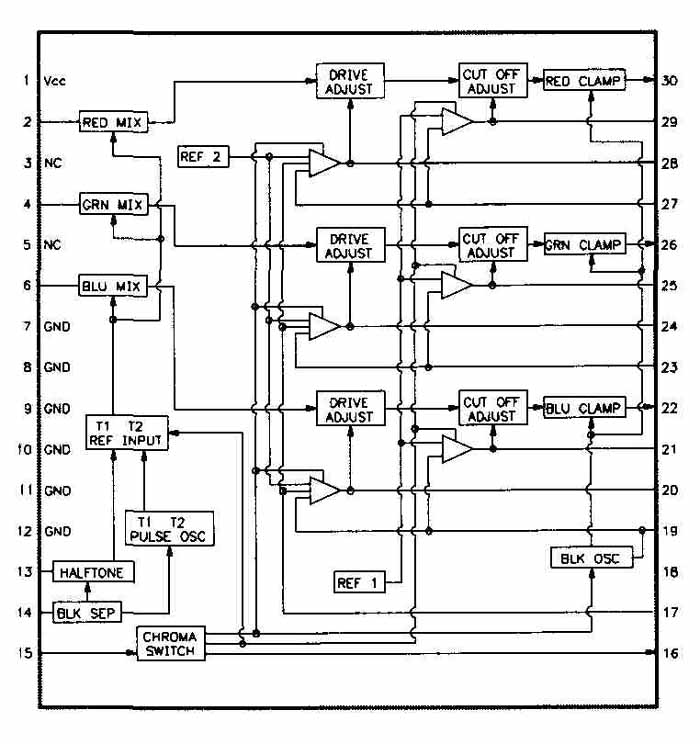
FIG. 25. Circuit using one IC for the color demodulators.
ICs
The receiver color sync section is often referred to as the chroma processor. Generally, some or all of the sync section is included in one or more ICs. FIG. 25 shows a circuit using one IC for the demodulators and the following color amplifiers. The demodulators are supplied by a voltage regulator that is also in the IC.
Additional Circuits
A television is too complex to require the examination of all of its circuits within a schematic diagram. At any rate, such a thorough examination is unnecessary when considering the actual function of the television set. However, let’s look at the block diagram of a typical receiver to examine automatic control circuits.
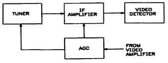
Automatic gain control (AGC) reduces receiver RF and IF gain when strong signals are received, so that they do not overload the amplifiers. FIG. 26 shows a block diagram of an AGC system. The sync pulse level alone is constant enough to be used as a measure of signal strength, since the video modulation level can vary widely during a broadcast. The sync pulse level is determined by separating the sync pulses at the gated AGC amplifier block. The clamping circuit forms the pulses into a DC voltage with a value of the received signal level, which is used as bias on the tuner and IF amplifier. The voltage polarity decreases the gain of the stages as signal level increases, so that the signal strength at the IF amplifier output remains stable.
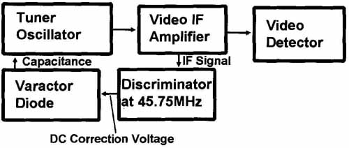
Automatic find tuning (AFT) is used to keep a television receiver properly tuned on a station. An AFT circuit is shown in FIG. 27. An IF signal from the video IF amplifier is fed to a discriminator tuned to the video inter mediate frequency (45.75 MHz). If video IF signal is at its ideal frequency of 45.75 MHz, where it should be, then the discriminator DC output voltage is zero and no adjustments are made to the tuner oscillator. If the tuner oscillator is off its proper frequency, the video IF signal will also be wrong; the result being that the discriminator will release a DC error signal of a polarity dependent on the tuner oscillator frequency. The DC error voltage is applied to the varactor, which changes the capacitance applied to the tuner oscillator, and returns the oscillator frequency to its correct value.
