THE LANG 20W CLASS-A MOSFET AMPLIFIER
BY K. LANG
THE GOAL OF THIS do-it-yourself project is to design a high quality amplifier at a reasonable cost, and without compromise. In order to achieve this goal some basic requirements must be fulfilled. The concept of this amplifier's circuit topology, and the choice of components, must be directed toward this goal right from the beginning.
The circuit should work with low open-loop distortion so we do not need to apply a lot of overall feedback around the circuit. Strong negative feedback causes stability problems, and increases transient distortion.
Therefore, the different stages must show good results using only a small local negative feedback, to achieve open-loop gain, with a minimum number of stages.
The output stage's circuit FETs (field effect transistors, Fig. 1) are especially suited for a class-A amplifier.
Aside from the low source current range, the FETs have an approximately linear transfer characteristic that shows up in the class-A operation: distortion goes toward zero with decreasing drive. In addition they can be easily driven, due to a theoretically infinite input impedance which simplifies the circuit as compared to bipolar transistors with their high power consumption.
Other advantages of these FETs are their lack of ‘secondary breakdown,' and their positive temperature coefficient. Both result in high operating reliability, without additional circuitry such as current limitations or ...
---Reprinted, with permission, from Elrad Magazine, Copyright 1985 Verlag Heinz Heise GMbH, Hannover, W. Germany. All rights reserved. ---
... temperature compensations, and an efficient paralleling of devices to in crease the overall current carrying capacity.
FETs do not store a charge during the transitions in the PN junction region, therefore they can be switched faster than bipolar transistors, which results in a higher limiting frequency. Their shorter recovery time, after an overdrive, has a positive effect on their transfer behavior for short overvoltages.
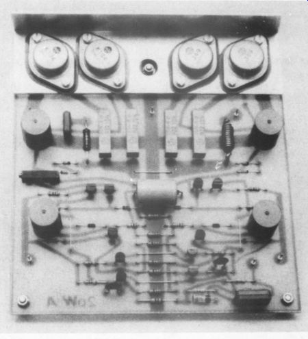
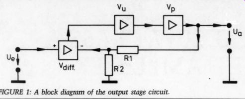
FIGURE 1: A block diagram of the output stage circuit.
Some disadvantages of a class-A output stage circuit are high power consumption, low efficiency and an unfavorable ratio of price to power output compared to other output stage circuits. The high price is mainly due to the costs of the necessary heatsinks and power supplies. How ever, all this together cannot convince a real class-A enthusiast not to build this circuit. Excellent sound is the most essential criterion. In addition, for a high quality output stage circuit, the price savings compared to the commercially available products is extremely good. Comparable class A amplifiers are twice as expensive.
Power Supply The cascode circuits of the low-level stages need a high voltage supply. On the other hand, the voltage supply to the output stage should be kept as low as possible due to power consumption problems. Therefore, two power supplies are used. This gives higher stability against oscillation and reduces crosstalk.
For the low level stages and the drivers, a standard dual power supply is used. The power requirement is very low, approximately 12mA per channel at + 24V. The output stage's power supply is unregulated and intentionally without current limitation, so as not to worsen the sound of the amplifier. The current requirement is approximately 3A to 6A per channel at +20V. [A regulated sup ply for the low-level section was published by James Boak in TAA 3/82, p. 9-Ed.] To protect the insensitive FETs against short circuit, or too low impedance, use fast-blow fuses. The circuit of the power supply is illustrated in Fig. 2.
Construction & Adjustment
Before the etched circuit board (ECB) is assembled some preparations need to be made. First drill the holes in the mounting bracket (shown mounted in Photo 1) and in the heatsink. For this purpose, we install the L-bracket on the empty ECB (Fig. 4) and drill the necessary holes for the FETs at the same time. This guarantees a better line-up of the ECB and the heat sink. Next we install the L-bracket on the external heatsink (see parts list) and drill the mounting holes through them at the same time.
The coil, L1, is built by winding 15 turns of #20 wire on resistor R29, and soldering it directly to the resistor leads.
The two power supplies should be built and checked in advance. By the way, two power supplies are the minimum solution. Using separate power supplies for each channel is recommended (four in all). Constructing a stabilized dual power supply according to one of the numerous standard circuits is easy, but it may be difficult to find a transformer for the output stage power supply. For stereo operation the output stage must deliver at least 7A to 8A, for mono at least 3A to 6A.
Now the parts of the amplifier must be soldered to the board in the known sequence, resistors, capacitors, diodes and transistors.
Note: solder the gate resistors of the FETs and the ceramic filter capacitors on the copper side of the ECB to minimize the interconnection wire length between these parts and the FETs.
The MOSFETs are mounted in the holes on the heatsink with mica insulators, insulating nipples and lots of silicone grease. The heatsinks and FETs are bolted to the ECB, and only then are they soldered. The mounting instructions are described in Fig. 3.
After inspecting the ECB for line up polarity, short circuits and breaks, we can start with adjustments. This is restricted by the adjustment of the quiescent current of the output stage.
First measure whether the resistance between the two connection points of the 10-turn potentiometer, P3, is zero ohm. If it isn't, P3 must be adjusted accordingly.
Now the power supply can be connected (without loudspeakers), and ...
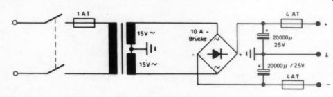
FIGURE 2: The power supply for the output stage. For the drivers and
input stages, a separate + power supply is needed.
-----------------
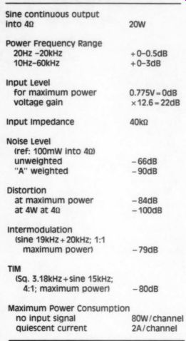
20W MOSFET POWER AMP PERFORMANCE SPECIFICATIONS
----------------
... the supply voltage can be switched on. If possible, for the first test, use two power supplies with power limitation to avoid potentially large damage in case of errors. You can test without the two supplies because the FETs are sturdy, but I recommend using two. If the test goes smoothly (without smoke), the output stage is ready for operation-in class-B.
The quiescent current is adjusted to 2A by connecting an ammeter in one of the supply wires of the output and by turning P3. The quiescent cur rent needs re-adjusting after the FETs and the heatsink warm-up (about ten minutes) to approximately 90 degrees Celsius (194F°). During this time the current should have dropped to approximately 1A to 1.5A.
The output stage can be operated with any other quiescent current between 0.0A and 2A, and will then be operated in class-B (respectively in class-AB). It now has a higher efficiency, but sounds worse than in pure class-A. Before operation, the output stage should be checked again with a voltmeter for offset voltage at the output. This voltage should not exceed 20mV.
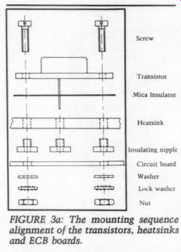
Transistor Mica Insulator Heatsink Insulating nipple Circuit board Washer
Lock washer Nut
FIGURE 3a: The mounting sequence alignment of the transistors, heatsinks
and ECB boards.
I recommend using heatsinks as side panels for installation in a box. Connect them with bars, and cut suitable plates for the top, bottom, back and front. The free space in the middle can be used for the power sup plies. The rectifier can be mounted directly on the bottom plate. The in put and output connectors, and the three fuse holders, should be mounted on the back plate.
Results
The description of this do-it-yourself project shows that an excellent class A amplifier can be constructed for audio applications with a relatively small number of components. The high quality of the amplifier is by no means the result of an innovative circuit design. It is due to the strict adherence of simple design rules: using moderate but correct amounts of negative feedback, avoiding TIM (transient intermodulation distortion) by pure passive bandwidth limitation, etc. However, the excellent test results are no guarantee for how well the amplifier sounds.
Personal listening tests are subjective and relevant, but cannot be technically measured. According to actual technical findings, however, the class-A amplifier produces a sound that listeners prefer over others. Finally it is worth mentioning that the best class-A amplifier sounds only as good as the loud speakers it drives. Also, because of the relatively low power output, high quality, high efficiency loudspeakers should be used (i.e., horns). Only then does the class-A prove its superiority. [Class-A is also fine in low power for multi-amped systems, and especially good for driving electro static loudspeakers.-Ed.| How Does it Work? In the block diagram of the amplifier (Fig. 1), are three intermediate circuits: differential amplifier, voltage amplifier and power amplifier. For a high open-loop-gain (Aol 100) the closed-loop-gain Acl can be determined approximately by:
ag = Ue _Rutha U. R,
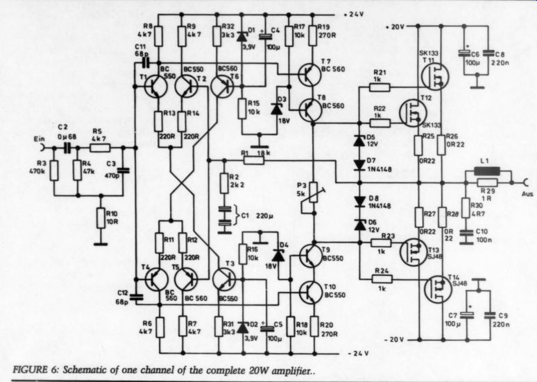
The complete design (Fig. 6) will be significantly simplified by this relation, and extensive calculations to find the total gain are unnecessary.
The circuit is remarkable, first of all, because of the completely symmetrical conception, which contributes considerably to reducing the distortions. The input stage is a differential amplifier: a nearly distortion free circuit without using any special measures. Therefore negative feed back, via the emitter resistors R1 to R14, is relatively low, resulting in a high open-loop gain.
The differential amplifier offers the additional advantage that the overall negative feedback can be applied, via a voltage divider, to the second input of the differential amplifier.
The two differential amplifiers operate with two constant current sources (R1 and R32, C4 and C5, T3 and T6 and D1 and D2). Here, the quiescent currents will be fixed and decoupled from the supply voltage.
The symmetrical design also simplifies the supply of base current to the input stage. The input is connected to ground through R14, R5 and R10, and is at zero volts, because no cur rent passes through these resistors when the input transistors are balanced.
The constant current sources are adjusted to approximately 1mA by R31 and R32. This is a good com promise between the noise of the transistors, proportional to the current, and the distortions, caused by the single-sided load of the differential amplifier due to the current requirement of the driver transistors.
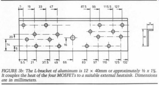
FIGURE 3b
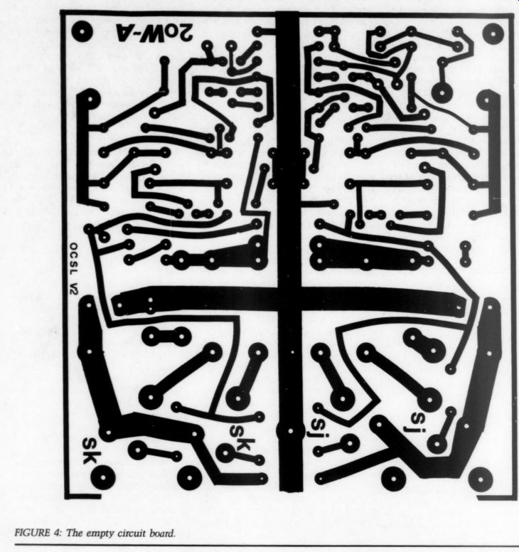
FIGURE 4: The empty circuit board.
The driver circuit is a bipolar push pull cascode circuit, consisting of transistors T7 to T10. Most of the design work is in this part of the circuit. The bipolar cascode was selected after extensively testing and measuring six different driver circuits. Simple push-pull circuits push pull Darlingtons or VMCS-driver types tested badly.
The cascode stages get their bias from the constant voltage sources, via R17 and R18, and D3 and D4. The cascode stages are driven with the voltage drop across the collector resistors of the differential amplifier.
The quiescent current through the cascodes will also be adjusted by that voltage, and depend on the quiescent current of the differential amplifier.
The emitter resistors R19 and R20, add a small negative feedback to the almost distortion-free cascodes. The quiescent current through the cascodes is approximately 10mA, to cover the current requirements at high frequencies of the FETs due to their channel capacities.
The quiescent current in the cascode stage is producing a voltage drop across P3, and this voltage is used to bias the output FETs. The quiescent current in the output stage can, with out problems, be adjusted between zero and 4A.
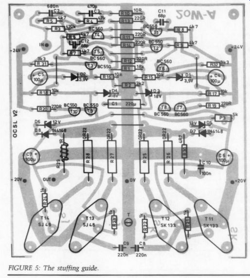
FIGURE 5: The stuffing guide.
The circuit of the output stage is simple: the source resistors R25 to R28 guarantee a small negative feedback, and compensate for variations between the different FETs. The resistors R21 to R24, and the capacitors C6 to C9 , , prevent the tendency toward oscillations of the output stage. They install as near as install as near as possible to the FETs. to the FETs.
The RL and RC networks, made up of R29 and R30, C10 and L1 at the amplifier's output, isolate the capacitive and inductive load represented by the loudspeakers, thus also reducing the tendency towards oscillations.
Protection diodes D5 to D8 prevent gate source voltage from rising too high in case of overdrive or short circuit of the output stage. The necessary output current, and the supply voltage of the output stages, are calculated as follows:
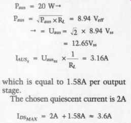
Paus = 20 W- Pass = (Poe xR, = 8.94Ver
= = Umus= [2 X 8.94 Vg
= 12.65Vy
= 3.16A
which is equal to 1.58A per output stage.
The chosen quiescent current is 2A
I DS_MAX = 2A +1.58A = 3.6A
The quiescent current is high so the FETs can still work, even at a minimum current of 0.4A, in a linear range. The minimum supply voltage results from the maximum output voltage, plus the voltage drop of the od in a hard driven:
Us = Uaus, + Ibsy,x X Rosy, =18.7V
The supply voltage chosen is +20V. The supply voltage chosen is +20V.
From the supply voltage and the quiescent current the maximum power consumption can be calculated:
P_v_max =2x20Vx2A =80W
This seems to be high, but it is unavoidable for a true class-A output stage. In addition, as is the normal case, power consumption is reduced considerably when the output stage is driven.
The last parts of the circuit are the input filter and the feedback path.
The input filter, built up by R3 to R5, and C2and C3, is a bandpass with a 1 bandwidth of 5Hz up to 60kHz.
--------------
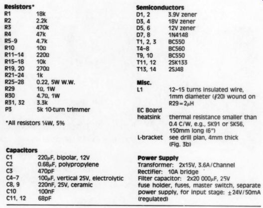
Parts List
Semiconductors
18k 3.9V zener 22k 18V zener 470k 12V zener a7k 1N4148 4 % 8CSS0 44 4, Ah ose g15-18 10k 25K133 R19,20 2700 2s)48 R21-24 1k goa 37 % JWWW. 11 12-15 turns insulated wire gz 4.70, WW 1mm diameter (20) wound on Rr31,32 33k R29=2uH P3 5k 10-turn trimmer EC Board heatsink thermal resistance smaller than
0. co 0.4 C/W, e.g., SK91 or SKS6, 150mm long 6 ”) L-bracket see drill plan, 4mm thick (Fig. 3b)
Capacitors
C. 2204F, bipolar, 12v
Power Supply
C2 0.68 uF, polypropylene
Transformer: 2x15V, 3.6A/Channel 3 470pF Rectifier: 10A bridge ca-7 100 uF, vertical 25V, electrolytic Filter capacitor: 2x20 000 uF, 25V 8.9 220nF, 25V, ceramic fuse holder, fuses, master switch, separate 100nF power supply, for input stage: +24V/50mA 68pF (regulated)
-------------------
Therefore, the bandwidth of the total circuit will be limited by passive components upwards as well as downwards.
This design is necessary to avoid a bandwidth limitation by the (active) high-pass of the negative feedback network, (R1 and R2, and C2). Such a bandwidth limitation in the negative feedback network is always a problem and easily leads to instabilities.
The upper limiting frequency of the passive input filter, in the range of 60kHz, lies considerably under the limiting frequencies of the active stages, and prevents problematical TIM distortion. The whole input filter is not connected directly to ground, but via the low value of R10, thus reducing the danger of ground loops and hum.
The negative feedback network, as already described with high open-loop gain, defines the total gain. With the indicated resistors it is adjusted to 13 times, but it is easily changed with a suitable resistor (i.e., in order to change the input sensitivity).
In this branch the capacitor C1 pro vides increasing negative feedback at low frequencies and theoretically an infinite negative feedback at DC volt age-gain is equal, 1=0dB. There fore, the output lies on the same voltage level as the input, namely on the ground level. O] Readers interested in constructing the Lang 20W Class A amplifier may express interest in circuit boards for the project by listing BK37 on a Fast Reply Card (estimated cost $10.50 each). Those interested in a complete kit of parts. (Estimated cost $260 per stereo amp with two power supplies.
----------------
Also see:
USING SOLID-STATE RELAYS: SAFE POWER CONTROL by L. B. Dalzell