A MOVING COIL PREAMP PART II
LET’s LOOK AT the complete MC preamp schematic (Fig. 1). I have connected four pairs of FETs in parallel, which become a good compromise as far as total drain current, cost and input noise are concerned. As I promised in the noise overview, you can do without electrolytics in the input stage by using only the lowest I_dss group (GR: 5-10mA) of the Toshiba FETs. You can use four pairs of the single devices (2SK147GR/ 2S5J72GR) I described in the preamp article or, if you have access to them, use two pairs of dual FETs: 2SK146GR/2S]73GR. The dual FETs have matched devices in one common case (Photo 4), but they only offer an advantage if the N-channel types are matched to the P-channel types. If not, the single devices will work just as well in this circuit.
Whether you use singles or duals is really a question of what you can find.
The GR group is specified at 5-10mA, and to get very low noise, they should be operated at a mini mum of 5SmA. By connecting four in parallel without source resistors, you might get, in the worst case, 20 40mA total drain current. This is too much variation, and to handle the drain current, you must get closer to the low-end than the high-end. Ideally, you should select devices with Ipss =5-6mA and connect these in parallel without source resistors. You might, however, need to buy many devices to find four within this range.
Instead, I have chosen a source resistor of 6.8 ohm, which slightly in creases the input noise but lets you use practically all devices from the GR group. Although this should as sure proper input stage operation, check the voltage drop across drain resistors R11 and R26. It should be 2-2.5V (20-25mA total drain current), but being 10% outside these limits doesn't seem to hurt the amp's operation.
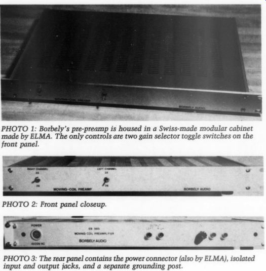
PHOTO 1: Borbely's pre-preamp is housed in a Swiss-made modular cabinet
made by ELMA. The only controls are two gain selector toggle switches
on the front panel.
PHOTO 2: Front panel closeup.
PHOTO 3: The rear panel contains the power connector (also by ELMA), isolated input and output jacks, and a separate grounding post.
To avoid excessively high current (and power dissipation) in the cascode transistors, connect two of the input devices' drains and feed separate cascode transistors (Q9 and Q10 on the N-channel side, and Q11 and Q12 on the P-channel side). For minimum noise, I have used extra filtering for the reference voltage of the cascodes.
Actually, I should also have reduced the voltage across the input FETs to avoid excessively high power dissipation. High temperature will reduce the effective gm and increase the FETs' gate leakage current, both of which tend to increase noise. The 15V seems to have an insignificant effect on the noise, yet helps keep the input devices in the linear range of their operation, so I opted to stay with the cascodes' original reference voltage.
The amplifier ’s second stage is the same as in the RIAA-1 amp (see the preamp article for a detailed description). The output stage uses the Hitachi MOSFETs (Photo 4), and these cannot be substituted by the bipolars used in the RIAA-1 amp. Adjust the bias with P1 to approximately 20mA.
For long-term stability, P1 should be a Cermet trimpot. A heatsink on the TO-220 MOSFETs is a must.
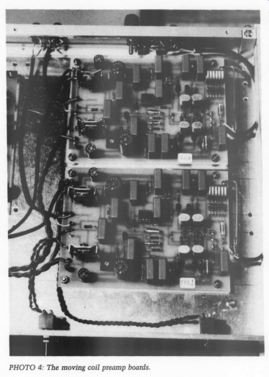
PHOTO 4: The moving coil preamp boards.
For pickup load switching, I added a DIL switch with up to six poles at the amp's input. I usually use the resistors shown in Fig. 1, but you can change these values to suit your MCs. You can also leave all switches in the “off” position if you need a high impedance load for your pickup! In this case, the load will equal RS, which I have chosen to be 47.5 k-ohm but which you can select as you wish. If you change your MCs frequently and don't want to go inside the amp to change the load resistor, add a small switch (gold-plated ELMA 01 or equivalent) on the back panel and arrange the load resistors on this switch. You can also add a second set of input connectors, connected in parallel with the main inputs and in which you can plug the necessary load resistors.
I have chosen a 0.0022 uF cap for the input. This might not be optimum for all MCs, so check the manufacturer ’s recommendations and change the value accordingly. The capacitor must be high-quality film, preferably polypropylene. The same goes for cap C, which connects the ground side of the input connector to the chassis. I am using a 0.01uF poly propylene (type WIMA FKP 2) in this position.
As I mentioned earlier, I compromised on the value of the feedback resistor (R31 =2.21 ohm). This will allow you to use a 43 ohm series feedback resistor for a gain of 26dB, and an 86 ohm for 32dB. These values solve the out put stage loading problems, but the offset problem remains. There is no practical way to adjust the offset by putting a trimpot in the source circuit. (You will notice there is a place for such a trimpot on the layout, and I use it in the higher impedance RIAA-1 version 2 [V.2] amplifier. I don't think you can find a 32/10 turn Cermet trimpot needed for this job.)
So, you must rely on the servo circuit. Using the LF411 here, with a minimum recommended load of 2k, you can easily calculate the amount of offset the servo can compensate:
V_out-max =13mV (9)
... where V_out-max is the maximum out put swing of the LF411, here assumed to be 12V. This doesn't sound like much, but I never had problems tracking the offset when the input FETs were from the same group. [ am afraid if the offset is higher, you must find either an op amp with higher current capability, or get FETs with better matching.
The equivalent noise circuit for the MC-preamp's input stage is shown in Fig. 2. The FETs are represented by their equivalent noise resistance, which, you might recall from our noise theory, is 34 ohm. The equivalent noise resistance of the entire input stage is calculated to be 9.5 ohm, that is, the input stage is generating the same amount of noise with shorted input as a 9.5 ohm resistor.
The equivalent input noise versus source resistance (Rs), as measured on several prototypes, is shown in Fig. 3. Notice the curve is very close to the theoretical one, going asymptotically to e, = 56mV, which is equivalent to the noise of a 10 ohm resistor.
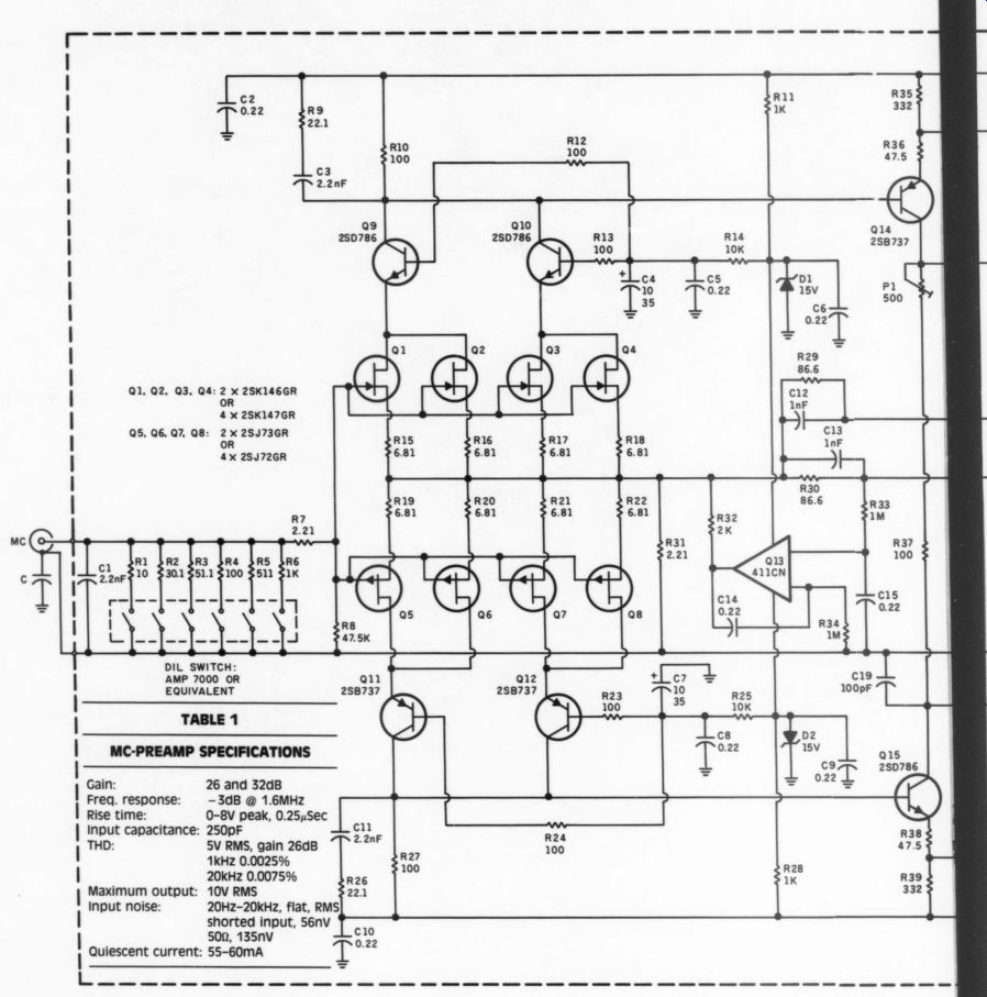
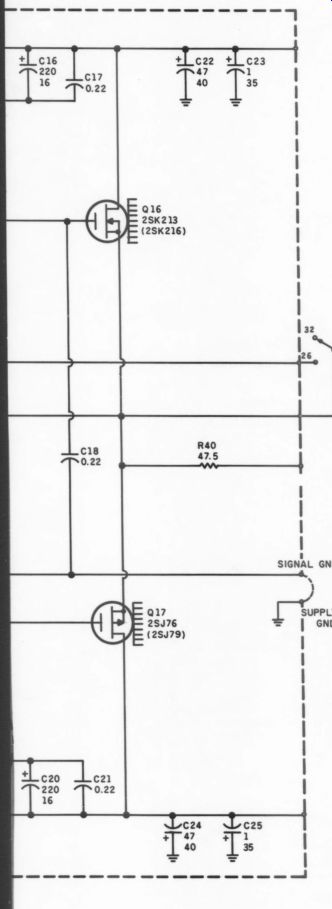
FIGURE 1: MC-preamplifier schematic.
Although not shown, the noise at 47.5 k-ohm is what is expected from a resistor of that value and with no sign of shot noise. I'm not claiming this is the lowest noise MC-preamp on the market, but it does offer excellent noise performance for pickups with sensitivities down to about 0.2mV.
Figure 4 shows the MC-preamp layout. In accordance with the wishes of the editor, I have changed the resistor spacing to 0.5 ”. This will allow you to use Resista ’s MK-3-type metal film resistors which Old Colony plans to standardize for future designs. Note the “clean ” signal ground on the board. You can connect this separately to the regulator board, but you must connect a 0.01 uF/160V polypropylene capacitor directly on the board between the signal ground and the power supply ground. This will avoid problems at high frequencies. As an alternative, you can connect the two grounds on the board, as shown on the stuffing guide (Fig. 5). When stuffing the board, be careful when you insert the input FETs. The stuffing guide shows the layout for the dual FETs. When using the single FETs, carefully consult the pinout in Fig. 14.
Power Supply
As mentioned earlier, one of the important factors in low-noise amplification is interference from power supplies. When you deal with extremely low levels of an MC-pickup, there should be practically no interference at all. Consequently, only the highest quality power supply is suitable for MC-preamps.
When I set out to design my power supply, I looked through my old sup ply designs. Instead of trying to up date these, however, I decided to use one of the excellent Sulzer designs in TAA. The final circuit is shown in Fig. 6, a modified version of the Sulzer circuit published by J. Breakall et al in TAA 1/832 It consists of a preregulator using the LM317/337 three-terminal IC regulators (Photo 5), and the op amp regulator using the NE5534. Unregulated input to the pre-regulators should be about 3V higher than their output, and the input to the op amp regulator should be about 3V higher than the final output. To build in some safety, I adjusted the pre-regulators for an output of approximately 28V for a final output of 24V. The rectified DC voltage of 32-33V comes from a transformer with 2x24V RMS secondary. Just as with the preamplifier, I used independent power sup plies for the two channels.
--------
------
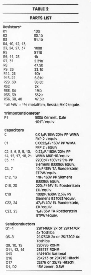
TABLE 2
PARTS LIST
Resistors* R1 100 R2 30.10 R3 51.10 R4, 10, 12, 13, 23, 24, 27, 37 1000 RS 5110 R6, 11, 28 1k R7, 31 2.210 R8 47.5k R9, 26 22.10 R14, 25 10k R15-22 6.810 R29, 30 86.60 R32 2k R33, 34 1 M-OHM R35, 39 3320 R36, 38, 40 47.5 ohm
*all aW + 1% metalfilm, Resista MK-2/equiv.
Trim potentiometer P1 5000 Cermet, Dale 101T/equiv.
Capacitors
C 0.01F/63V/20% PP WIMA FKP 2 /equiv C1 0.0022 uF/160V PP WIMA FKP 2 /equiv
0.22,F/160V/20% PP WIMA MKP-10/equiv.
2200pF/160V/2.5% PP Siemens B33063/ equiv.
10 uF/35V TA Roederstein ETPW/equiv.
1nF/160V PP Siemens B33063/equiv.
220uF/16V EL Roederstein EK/equiv.
100pF/630V/2.5% PS Siemens B31063/equiv.
47 uF/40V EL Roederstein, EK/equiv.
1 uF/35V TA Roederstein ETPW/equiv.
C2,5,6,8,9,10, 14,15,17,18, 1 C311 Ca,7 C12, 13 C16, 20 C19 C22, 24 C23, 25 Semiconductors Q1-4 2SK146GR 2x or 2SK147GR 4x
Toshiba 2SJ73GR 2x or 2SJ72GR 4x Toshiba 2SD736
ROHM 2SB737 ROHM LF411CN National 25K213 or 25K216 Hitachi 25J76 or 25J79 Hitachi 15V zener, 0.5W Q5-8 Q9, 10, 15 Q11, 12, 14 Q13 Q17 D1, D2
------------
Here are the formulas to calculate the necessary resistor values should you choose voltages different from the ones shown in Fig. 6:
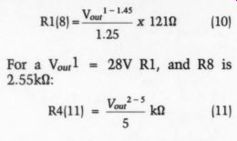
Formula 11 is valid when R3 and R10 are 1 k-ohm and the reference voltage is 5V. For a V_out=24V R4, and R11 is 3.8 k-ohm.
The opamp regulators' reference voltage is supplied by the LM336Z-5.0 reference diodes. These “diodes” have a tolerance of +4%, so the absolute value of the output voltage can be 4% off the nominal value: 24V, +/- 1V. If you are concerned with the absolute value and/or with the plus and minus sides being equal, you'll have to trim resistors R3 and R10.
Layout for the regulator is shown in Fig. 7. You will need two of these boards for an MC-preamp. The stuffing guide is shown in Fig. 8. Note I have used a common heatsink (Photo 6) for the preregulator and the series pass transistor on each side (Fig. 9).
Make sure you mount these with mica and nylon screws, and use a generous amount of silicone grease on both sides of the mica insulator.
No fuses are shown in connection with the power supply. I recommend, however, putting a fuse in the plus and minus leads, between the power supply and the MC-preamp. The quiescent current consumption of the MC-preamp is 55-60mA, but will rise to approximately 100mA with full drive. You should, therefore, fuse the circuit with 200mA medium blow fuses.
Naturally, you can use this supply for other projects, such as instruments and crossovers, by scaling the voltages for your particular application. Before you install the power supply, test it with a load resistor, a voltmeter, and preferably a scope.
The load resistor should reflect your application's final current demand. I also measured the power supply noise, using a low-noise preamp and a 20Hz-20kHz noise filter. The RMS noise output was 1-2uV. This should satisfy just about all audio application requirements.
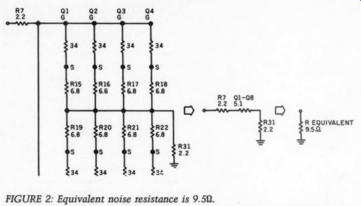
FIGURE 2: Equivalent noise resistance is 9.5 ohm.
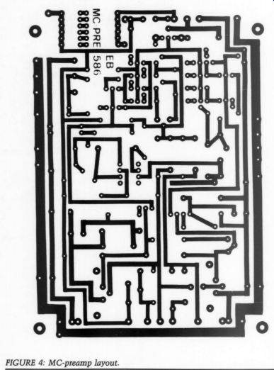
FIGURE 4: MC-preamp layout.
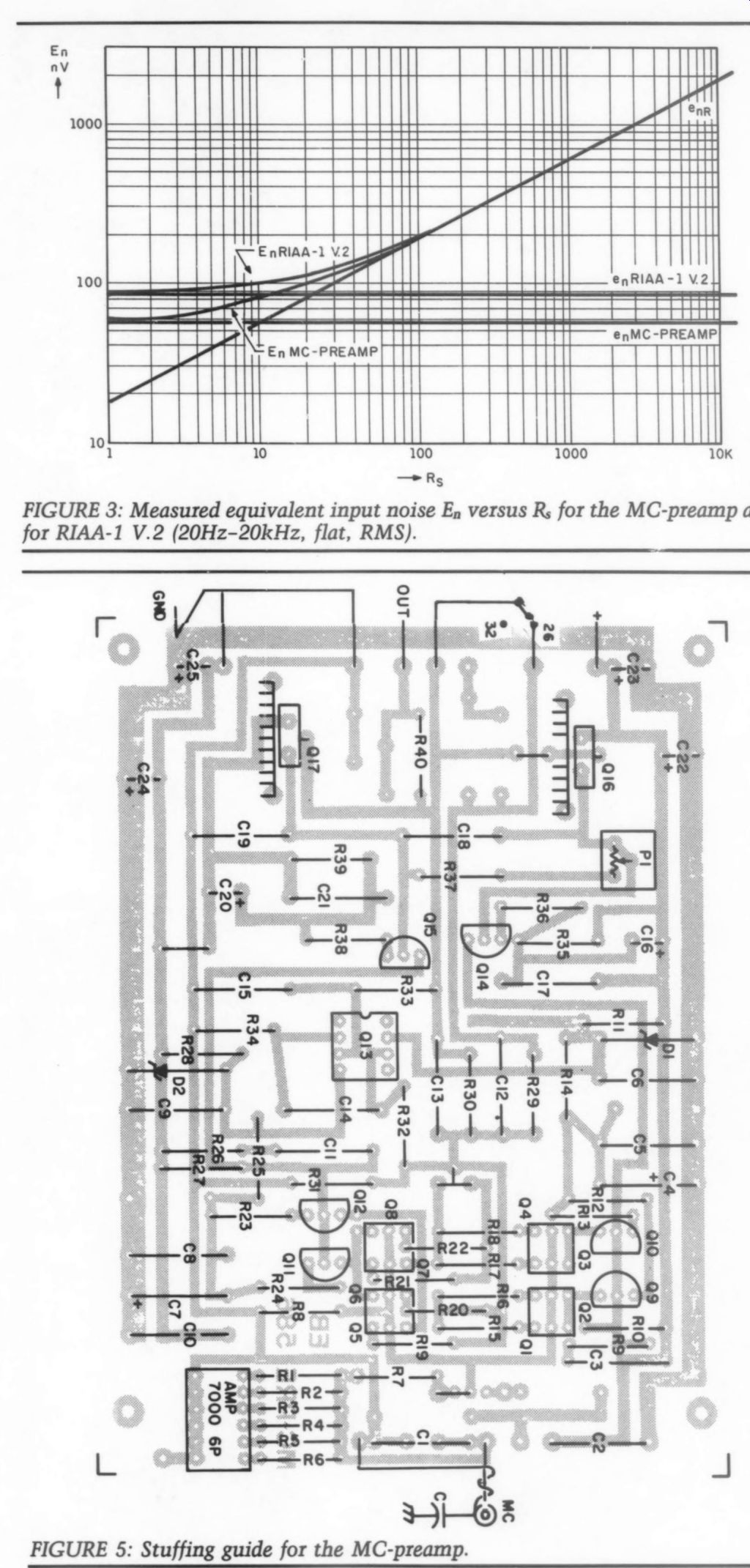
FIGURE 3: Measured equivalent input noise E, versus Rs for the MC-preamp and for RIAA-1 V.2 (20Hz-20kHz, flat, RMS).
FIGURE 5: Stuffing guide for the MC-preamp.
The wiring diagram for the MC preamp is shown in Fig. 10. I have been using a one-unit high, 260mm deep, 19 ” box for the pre-pre, and have considerable space to spare. I put the gain switches on the front, and gold-plated phono connectors for input and output on the back panel.
The transformer, like the preamp, is in a separate box, interconnected with a 6-pin LEMO connector (Photo 7) to the pre-pre.
Medium Output MCs
Although the previously-described MC-preamp can take care of just about all MCs, you do not need it when you have a medium-to-high output pickup and an EB-585 preamp.
A medium output has been defined as, you will recall, 0.5mV @ 5cm/sec RMS lateral velocity. With these pickups, you need approximately 20dB extra gain in front of the RIAA stage or, as I propose here, built into the RIAA stage.
In theory, if you were only interested in MCs, you could use the MC preamp in Fig. 11 (TAA 4/86) as an RIAA-1 stage. If you are like me and prefer to have both MM and MC in put, you can't use the MC-preamp without modifications. Four pairs of FETs have an input capacitance of approximately 250pF, and this might be too high for some MM-pickups. Also, the MC-preamp can't drive the feed back network in pure class A beyond approximately 1V RMS, which is not enough for the RIAA-1 stage used for MM-pickups. For MMs, the single pair is the best solution, as used in the RIAA-1 stage of the preamplifier.
For MCs, the four-pair input circuit is the best, as shown in the MC preamp. For a circuit that must work with both, a two-pair input is the best compromise.
Figure 11 shows the complete schematic of the high-gain version of the RIAA-1 amplifier. Notice the in put stage uses two pairs of single FETs (2SK147/2SJ72) or one pair of dual FETs (2SK146/2sj73). Since the MC-input is for medium-to-high out put pickups, it is not necessary to use very low values for the feedback and source resistors. The relaxation of the first makes it easier to drive the feed back network and to track the input offset. The second gives you a wider choice of input devices. Although I recommend you stick to the BL group for best low-level linearity, you can mix BLs with GRs in your circuit. I have also mixed two BLs on the N channel side with one GR and one V on the P-channel side, but this is a worst case situation and should be avoided.
The feedback network, which uses a 6.80 shunt resistor, allows you to select 20, 30 or 40dB gain. The lowest gain position is for MM-pickups and for high output MCs, and the highest gain position is for medium output MCs. With such a closed-loop gain (40dB), you might be wondering about the performance of the RIAA-1 V.2. Naturally, the THD of the RIAA 1 V.2 deteriorates somewhat at the highest gain setting because of reduced feedback. It's still only 0.0035% at 5V RMS and 1kHz, which I consider negligible. More importantly, I confirmed with extensive listening tests that there was no sound quality deterioration.
The RIAA-1 V.2's noise performance is indicated in Fig. 3. The equivalent noise resistance of the in put stage equals 220, with a theoretical value of e, =84nV. Actual measurements, as shown in Fig. 3, come very close to confirming this value.
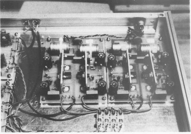
PHOTO 5: Separate power supplies for each channel are provided with
full regulation and individual fusing for each of the four supplies.
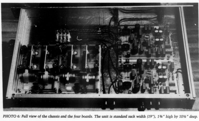
PHOTO 6
The input can be switched be tween MM and MC with an on-board switch (gold-plated, 0.1” spacing), or with a switch you can put on the front panel and wire to the board with a three-wire shielded cable (connect the shield to the input ground on the board). The MM input has 47.5 k-ohm load, installed permanently. The MC input, like the MC-preamp, can be loaded with up to six different resistors. Note that capacitor C1 is equal to C_load - C_in, where C_load is the recommended load capacitor for your MM-pickup and C1, is the input capacitance of the amplifier (C_in= 120pF). C2 is again 0.0022 uF, but you should adjust it according to the manufacturer's recommendations. Both capacitors must be high-quality film types.
The 75 usec high-frequency rolloff is provided by R36 and C26. I reduced this network's impedance to reduce the source impedance as seen by the RIAA-2 amplifier, which in turn reduces the noise in that stage.
As you did with the original preamp, I suggest you check the RIAA accuracy with an inverse RIAA network when you install this high-gain version of the RIAA-1 amplifier. If necessary, trim the accuracy with R36.
Layout for the RIAA-1 V.2 is the same as the MC-preamp (Fig. 4). The stuffing guide is shown in Fig. 12.
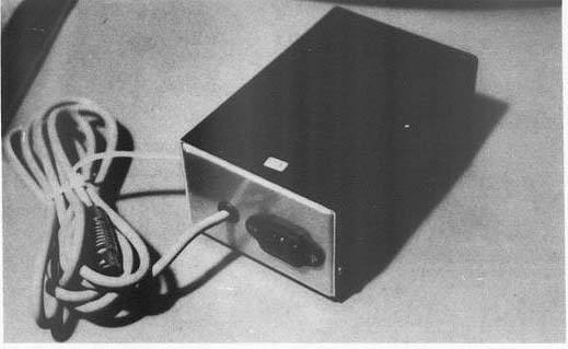
PHOTO 7: The raw DC power supply is housed in a separate enclosure with
a six-pin locking connector, a modular AC power connector with its on/off
switch on the front end.
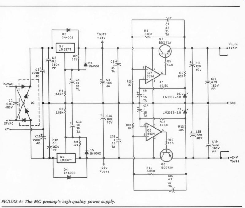
FIGURE 6: The MC-preamp's high-quality power supply.
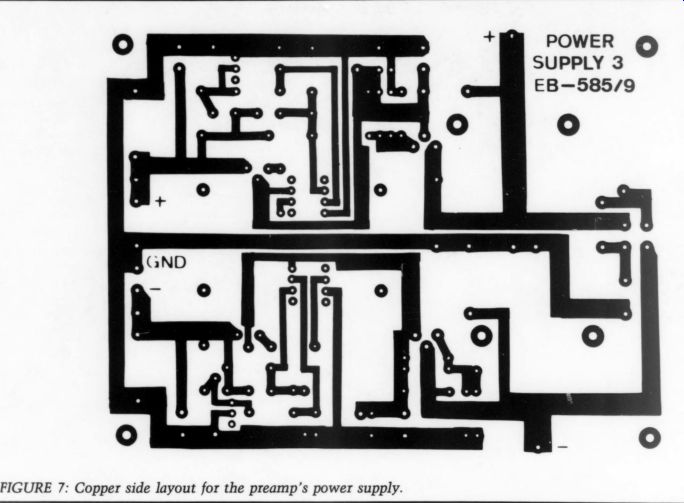
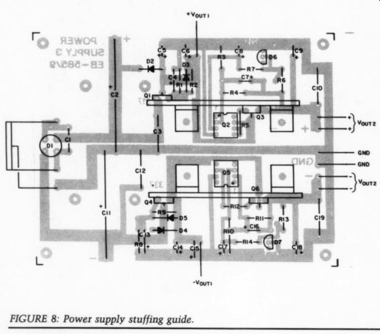
FIGURE 7; FIGURE 8: Power supply stuffing guide.
Again, the stuffing guide shows dual FETs at the input. If you use single FETs, carefully study the pinout diagram in Fig. 14.
Unfortunately, using the MC-pre amp layout for the RIAA-1 V.2 has a drawback: its size. Because it is more than an inch longer than the original RIAA-1, you might have problems re placing it with this larger board in an existing box. Two possible solutions immediately come to mind when you use the box and mechanical lay out indicated in my preamp article.
(If you don't need the tape buffers, the problem doesn't exist; the RIAA-1 V.2 and the RIAA-2 boards will fit nicely in the available space.) If you need the tape buffers and want to use the RIAA-1 V.2 boards, consider moving the power supply boards out of the preamp box and in to the separate transformer box. This will free up an entire column of space in this box size and allow you to put in many extra features, including the tape buffers. As an alternative, consider making a special layout for the RIAA-1 V.2 that fits into the place of the original RIAA-1 board. You won't have a problem if you have a dual-height box because you can stack two boards on top of each other.
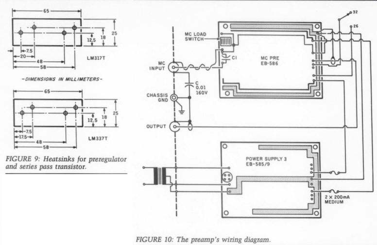
FIGURE 9: Heatsinks for preregulator and series pass transistor.
FIGURE
10: The preamp's wiring diagram.
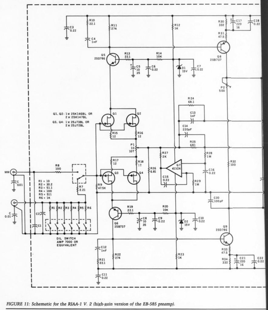
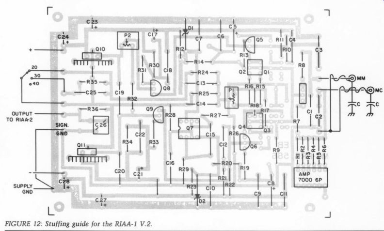
Fig 11; Fig 12
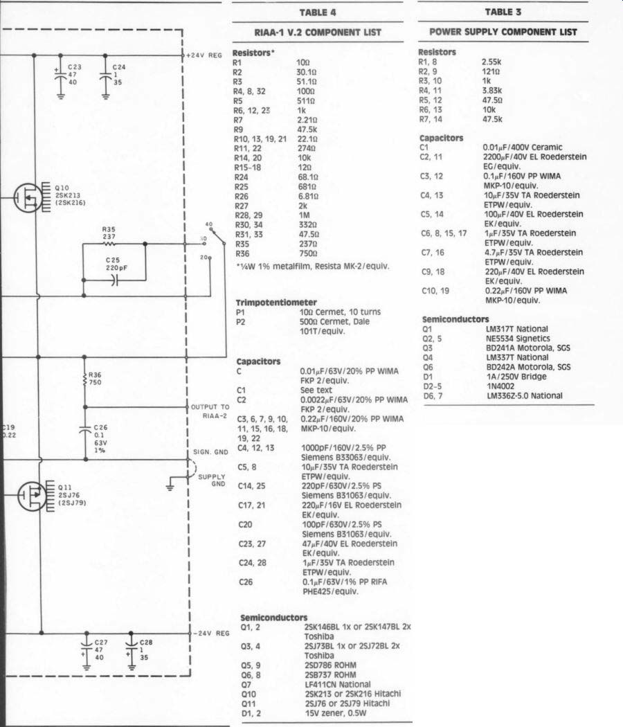
TABLE 4 --- RIAA-1 V.2 COMPONENT LIST
TABLE 3 --- POWER SUPPLY COMPONENT LIST
Refer to Fig. 13 before wiring the KIAA-1 V.2 board into the EB-585 preamp. I included some changes in this wiring diagram that also apply to the original preamp, including wiring of the RIAA-2 stage output, the 1k resistor in series with the volume control and the twisted pair of wiring to the line amp input.
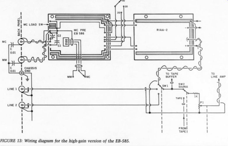
FIGURE 13: Wiring diagram for the high-gain version of the EB-585.
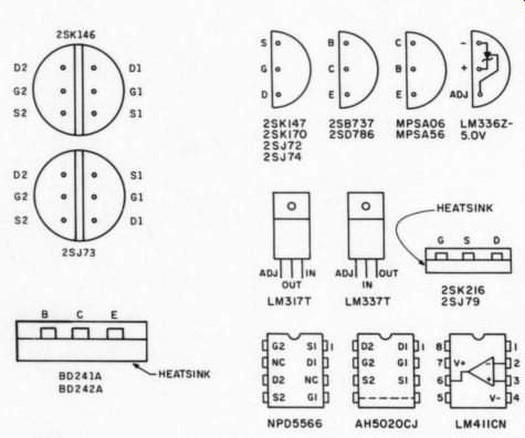
FIGURE 14: Pinout devices used in the MC-preamp, the power supply, and RIAA-1 V.2. Except for the 317/337 regulators, all devices are shown from the bottom view.
Conclusion
I apologize if you have already built the regular RIAA-1 input stage when you really needed the high-gain version. At the time I submitted the pre-amp article, however, I hadn't decided to offer this high-gain version.
I believe the approach presented here is the best compromise for sound quality, which is, after all, what this hobby is all about. Building the preamp with or without the MC-preamp, as dictated by your particular pickup(s), will, I believe, give you some of the best sound quality available today. Good luck with your project.
ACKNOWLEDGMENT: Dr. Kalman Molnar, consultant, reviewed the chapter on basic noise theory and suggested many excellent improvements. I greatly appreciate his contribution.
REFERENCES
1. TOM, “The Koetsu Rosewood Signature Review, ” The Absolute Sound, Vol. 10, Issue 40, Winter 1986.
2. Breakall, J. et al, “Measuring Power Supply Output Impedance, ” TAA 1/83.
By Erno Borbely
----
Also see:
PREEMINENT PHONO PREAMP, By John H. Roberts
A 500W MOSFET POWER AMPLIFIER PART II, By H. J. Heckert