ADVANTAGES OF “balanced”' transmission lines, chat is, lines where the A and B wires have equal impedances to screen or ground, have been well known to communications engineers since serious commercial services began. Despite the occasional phoney use of the term by the advertising fraternity to hype another characteristic altogether, 'balanced' enjoys general acceptance in the audio world.
Searches in my limited library have not uncovered a first use, but if I say it goes back to the early 1930s I'm sure one of you will do my job for me and produce a definitive reference.
Since the original method of obtaining the balance was by center-tapped transformers, the application to the in put and output of amplifiers followed predictable paths. Microphones, particularly ribbon types, benefitted audibly in freedom from hum and interference, and it was not long before designers produced whole amplifying systems which were balanced throughout. Ad vantages were not always logically linked to the true balance concept--sometimes elegance was as much a parameter as technical benefit! Unfortunately, transformers--particularly wide-band types-have always been expensive and have problems of inductance, self-capacitance and shielding which negate some of the balance advantages unless they are very care fully designed and installed. The transistor and op amp have given unlimited freedom to designers to get their balancing act together, and this little de sign comprising a send and receive module gives amateurs a flexible answer to the problems of converting un balanced signals to balanced and back again. It can be built to incorporate gain if required and to match any reasonable impedance.
--------------
For maximum common mode rejection, R1 + R2 = R3
Gain (dB) = 20 log (R1 + R2)/R2
Output Z = R5 + R6 (each 22)
Receiver: =
Input Z = R1 R2 + R4 A line input Z = R1 B line input Z = R2 + R4
For unity gain: R1 = R2 and R2 = R4, with R2 + R4 = R
Values for unity gain throughout and 600-ohm line:
R1 = 0 (i.e, a link) R2 = 10k R3 = 10k R4 = 47k (nominal value)
R5 = 300
R6 = 300
C1, C2 = 0.0uF ceramic disc
R1 = 300 R2 = 150
R3 = 300 R4 = 150
C3, C4 = 0.01uF ceramic disc
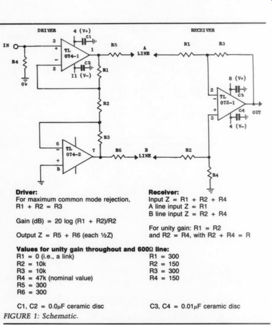
FIGURE 1: Schematic.
-------------------
Creatures of Habit
First the schematic, Fig. 1, which shows one channel of send and receive.
The values of R1, R2, R3, R5 and R6 are first calculated following the simple formulas shown. For example, in my prototype I chose unity gain for the driver and a line impedance of 600-ohm2-no magic in that, but communication engineers are creatures of habit. Thus, from the formulas, R1 = 0, R2 = R3 (chosen at a reasonably low value of 10k) and R5 = R6 = 3009. At the receive end, R1 = 300 ohm and R2 = R4 = 1500. R3 determines the gain, so for unity it is 300-ohm as well.
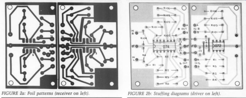
FIGURE 2a: Foil patterns (receiver on left). FIGURE 2b: Stuffing diagrams (driver on left).
Figure 2 shows the design and layout of a simple board which can be cut to provide the two modules, each giving two channels. You can leave the cut ting until you have finished construction, since this makes testing easy. As well as the input and output terminal pins, I used pins in the R1, R2 and R3 positions (R101, R102 and R103 for the other channel) on the driver module so that I could experiment with gains and impedances. The line terminals are aligned for foolproof connection, and the + Vg and -V; 15V supplies can be supplied from either end over the line cable.
If this upsets you, use separate supplies, but I would comment that communication engineers have been using the line supply concept over consider able distances for many years with no problems. Purists may query the need for two “links” on the simple receiver board. This is because the cussed TL072 has its (+) and ( -) supplies on the opposite sides of the IC from the TL074, and I considered the input pin symmetry to be more important.
A picture of the finished pair of boards is in Photo 1, and reference to this and the stuffing guide should make construction simple. Fit the two links on the receiver board first; C3 and C4 are in slightly different staggered positions on the prototype photo, but the board and component guide are easy to follow. Usual soldering precautions and care are mandatory, particularly on the IC socket pins. Check the finished board with a magnifying glass.
Worst Case Scenario
Power supplies are, as mentioned, (+) and (-) 15V. If these are not available at either end of the system, batteries can be used. Requirements are 8mA at the driver and 5mA at the receiver.
Feeding the total 13mA over the line using separate conductors is the obvious way, and in the prototype I purposely used a flat seven-wire ribbon cable to give the worst test conditions.
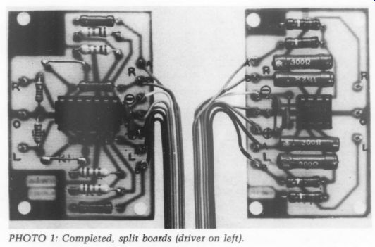
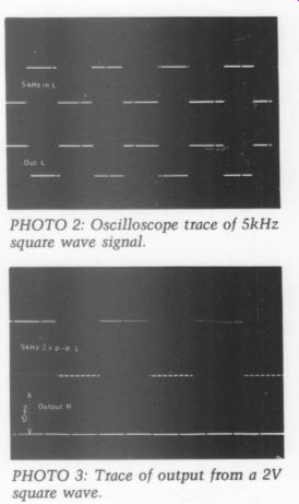
PHOTO 2: Oscilloscope trace of 5kHz square wave signal.
PHOTO 3: Trace of output from a 2V square wave.
The choice can be a six-wire shielded cable, using the shield as 0V. This should be impervious to any sort of in interference. If you decide batteries are a bit doubtful for continuous 13mA drain, then you could use a small stabilized power pack instead. C1-C4 are a precautionary decoupling design point which augments any other components in an outboard power supply.
An oscilloscope trace of a 5kHz square wave signal on one channel (Photo 2) shows input and output at 0.5V peak-to-peak. You will notice that the system is phase inverting; if this is not acceptable, then reverse each signal pair between the driver and receiver, A to B. In the photos, I have shown a straight connection for test purposes.
Don't Be Misled
Photo 3 shows the output from a 2V square wave on one channel with the other channel carrying no signal, and the trace blown up to 10mV sensitivity. To add insult to injury, I left the ribbon cable in a heap on the bench and turned on a portable TV, an RF genera tor and an electric drill before I took the trace photo. The only time I noticed any reaction on the “quiet” channel was when I was careless with my oscilloscope grounding-and that reminds me to mention that you should take care with tests on a balanced line with unbalanced test equipment: you can easily be misled.
ACKNOWLEDGMENT
My thanks go to Reg Williamson for his invaluable support.
++++++++++++++++
Also see: