BY ANDREAS SCHUBERT
PARALLEL OR SHUNT voltage regulators are uncommon in electronics, al though they offer advantages over series or pass regulators for audio applications.
Figure 1 illustrates how a standard volt age regulator works.
The raw supply usually consists of a power transformer, a bridge rectifier, and a large electrolytic capacitor. It de livers DC voltage, which varies with line fluctuations, and has a superimposed AC ripple dependent on load cur rent and charge capacitance. The regulator's task is to maintain a stable out put voltage, independent of load variations. It must have low output impedance, independent of input voltage changes, and high supply rejection. The regulator needs high internal feedback to work as intended. It is usually constructed as an emitter follower, with a differential amplifier or operational amplifier as the regulating device.
We can see from this scheme the audio circuit's bias current must flow directly through the regulator. Changes in the circuit's bias current due to an audio signal becomes an integral part of the regulators feedback loop. We can not guarantee the signal current is unaffected by the regulator's strong negative feedback.
In low feedback circuitry the goal is to minimize feedback generated effects, not only in the amplifier, but also in the supply design. Parallel regulators (Fig. 2) are one way to do this. The series regulator (Fig. 1) is substituted ...
--------------
ABOUT THE AUTHOR: Andreas Schubert is 29, and has a degree in electrical engineering from Technische Universitaat Berlin (FGR). He works for a well known West German audio amplifier manufacturer.
-----------
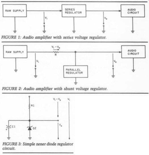
FIGURE 1: Audio amplifier with series voltage regulator.
FIGURE 3: Simple zener diode regulator circuit.
---------
... with a shunt regulator and a resistor R, which provides the necessary voltage drop between the raw supply voltage and the desired output voltage.
In this case, the audio circuit's bias current doesn't flow through the regulator, but is supplied by the raw sup ply via resistor R. The shunt regulator can only sink current, whereas the series regulator sources current. The circuit maintains a stable output volt age with low internal impedance. One disadvantage: regulators have a much higher idle power, due to a sort of "Class A” operation. They are, to my knowledge, not available as integrated circuits. Symmetrical supplies with positive and negative output voltages, Figures 1 and 2, can be completed with negative regulators in a mirror-imaged manner.
Circuits, such as the one published by R. N. Marsh (TAA 1/88 p. 26 and 4/88 p. 46) are not parallel regulators.
They provide a low impedance sym metrical ground to a single ended power supply, and need a pre-regulator which is actually a series regulator.
Practical Circuits
The simplest parallel regulator consists of a zener diode and a resistor R1. (Fig. 3.) A capacitor C can be connected for noise reduction. Figure 4 illustrates a typical V/1I transfer function for this type of diode.
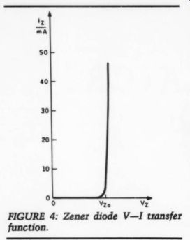
FIGURE 4: Zener diode V-I transfer function.
If the voltage across the diode junctions is raised from zero, very little current flows through the chip, until a certain break point is reached. Above this value, near the nominal zener voltage Vy the voltage cannot be raised much more, and zener current rapidly in creases. The diode acts as a constant voltage generator, because large changes of current cause only small voltage variations, i.e., the dynamic resistance dv / dl is low.
In the circuit (Fig. 3) a raw supply's excess voltage is dropped across resistor R1 by bias and load currents. This resistor's value must be chosen so that voltages and all load currents:
R1 = (Vipin = Vol / (lomin + 12min) Lin is the minimum allowable zener current, which depends on the diode type, usually in the 1-10 mA range.
With no load connected, the diode must sink the maximum idling current of:
Ime = (Vina = Vol / R1 so that maximum diode power is:
Poona = Vo X Lona Idling power obviously can be very high. Such a simple circuit is not there fore, suitable for high supply current With the addition of just one npn (power -) transistor Q and a resistor R2 (Fig. 5) a small power zener can be used, and high load currents are sup plied. Output voltage is now V, = V, + Vp due to the additional base-emitter voltage drop of Q1.
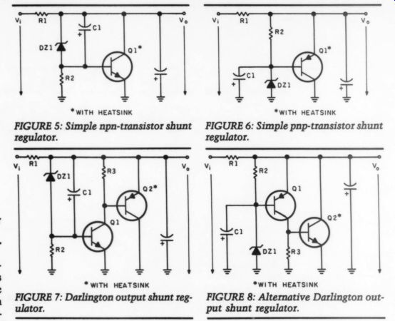
FIGURE 5: Simple npn-transistor shunt
FIGURE 6: Simple pnp-transistor shunt
FIGURE 7: Darlington output shunt regulator.
FIGURE 8: Alternative Darlington out put shunt regulator.
Again, R1 is dimensioned to supply constant V,, at minimum input voltage V,,, and maximum load current L,,.:
R1 = Vimin - (Vz + Viel] / lomex + Yzmin) and R2 is made R2 = Vg; / I; tO supply zener diode bias and provide base emitter voltage of Q1.
Bipolar transistor V1; is typically 0.6 to 0.7V.
Capacitor C serves to reduce noise. The circuit can also be arranged with a pnp transistor (Fig. 6).
We can reduce output impedance and improve supply rejection with Darling ton-connected transistors. Figures 7 and 8 show two examples which work well.
Additional resistors R3 speed up off drive for transistors Q2 and can be about 1k-ohm. These transistor circuits offer good performance with few parts.
Advanced Circuits
A regulation amplifier improves operation. It consists of a differential pair of transistors (Fig. 9). The zener diode generates reference voltage, and is connected to the non-inverting input of the differential amplifier Q1, Q2. Output voltage is measured and fed back to the inverting input by voltage divider R4, R5. Q2 supplies base current for shunt transistor Q3 to control the output, so that:
Vo = Vz x [1 + (R4 / RS]
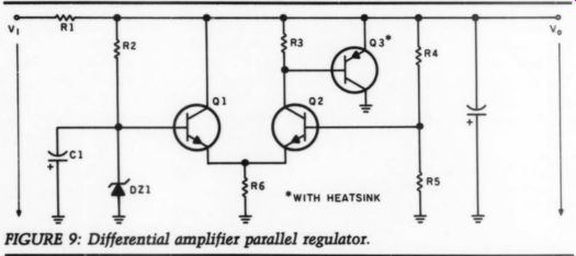
FIGURE 9
PARTS LIST: 2 x 30V 1A center tapped 1N4002 (100V, 1A) or equivalent dark red LED, 1.6V forward voltage TL O71 LF 356 1000, 10W 1 k-ohm 4.7k-ohm 1k, 1W 10ka linear operation 47uF, 16V 10,000uF, 63V 10,000.F, 40V BDW 84 pnp Darl. or equivalent BDW 83 npn Darl. or equivalent BC 560 C low noise. pnp 45V, 100mA or equivalent tor currents, and becomes R6 = (V; - Vas) / Ue.
You can chose I- in the range of 1-10mA.
R2 must supply zener current I; and becomes R2 = (V, - V;)/I;.
For base currents compensation, R4 should be equal to R2. Again, R3 speeds up off-drive for Q3. Finally, make R1:
R1 = (min = (ome + 2c + I)
Figure 10 illustrates an elegant regulator with just one operational amplifier A1 and a (power -) shunt transistor Q1. The circuit works similar to that in Fig. 9. The formulas given apply correspondingly. Two or more diodes, D1, D2, must be inserted to enable A1 to drive Q1 with its voltage supply connected to the regulated out put. This circuit offers excellent performance with few parts. You can try it with most op amps. For output voltages above 35V, a zener diode D, must be added to the negative supply line of A1 to limit its operating voltage.
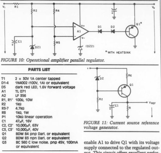
FIGURE 11: Current source reference voltage generator.
A Different Reference Source
The zener diodes should be eliminated as reference voltage generators to reduce output noise. A means of establishing a constant voltage is loading resistor R with constant current I;, so Uy, = R * Iz. A transistor current source (Fig. 11) can supply this current. Resistor R; sets; = (V; -Vg)/Rg so that V; = (R / Rg) x (Vz = Vg).
The zener diode in this case generates only reference voltage for Q1. Capacitor C1 can easily shunt noise in I; S and Ug. R; determines zener current I, = - Vs) /R, Forward driven light diodes, for in stance dark red: U;, = 1.6V, red U; = 2.0V, can take the place of the zener, and produce lower noise.
This reference voltage source can be used with circuits in Figs. 9 and 10, where the combination of R2 and D is replaced by the arrangement of Fig. 11.
Negative Output Voltages
All regulators described above can also be used for negative input and output voltages. All npn transistors must be substituted by pnp, and all pnp devices by npn. The polarity of all diodes and electrolytic capacitors must be reversed. All formulas apply correspondingly.
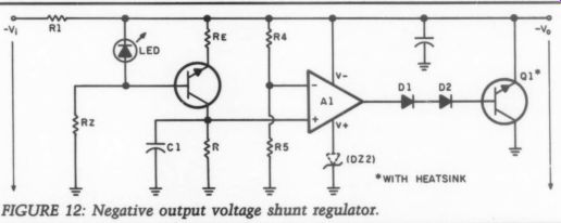
FIGURE 12: Negative output voltage shunt regulator.
Figure 12 shows a negative regulator, which is combined from Figs. 10 and 11. The supply voltage of A1must have correct polarity.
Design Example
One of my friends uses the circuit in Fig. 8 with a 24V, 150W power trans former to drive his NAIM preamp. A charge capacitor of 10,000uF, 40V is connected to the bridge rectifier and followed by a 110, 10W resistor. The zener is a 27V type giving an output voltage of about 28V, rather than the original 24V. The zener is buffered by a 10yF foil capacitor, and the output by another 10,000 uF, 40V electrolytic. A low noise BC-560-C transistor drives the well-known 2N3055 output device.
R2 is 2200, and R3 1k.
My friend reports distinct improvement in clarity and detail, compared to the original LM 317 regulator.
Spatial reproduction also was enhanced.
Using the low current gain 2N3055 alone (Fig. 5) reduced improvement.
The regulator (Fig. 12) supplies sym metrical output voltages adjustable from 10V-30V with potentiometer P1. Reference for the negative side is derived from the positive output voltage, keeping both outputs equal. The operational amplifier for the circuit's negative part should have a common mode input voltage range up to the positive supply voltage, because the differential inputs are at ground potential, as is its supply.
The diodes at the op amp's outputs can be omitted, because the shunt transistors are Darlington devices with base-emitter drop of 1.2V. They should be mounted with heatsinks. Maximum output current is about 100uA at 30V and 200uA at 15V. Current can be increased by reducing the two input resistors' value. Input voltage can be reduced, if only low output voltages are required.
The supply's negative side can be omitted if no symmetrical output volt age is needed. It is possible to experiment, for example, with different capacitors, and so forth. A parts list is given below.
Conclusion
I have tried to guide your interest into a relatively uncommon field, shunt voltage regulators for audio use.
Equipped with these figures and formulas, you can attempt to set up such a regulator for your preamp, for in stance. The raw supply, rectifier, and charge capacitor can be unchanged in most cases. It's useful to multiply sup ply capacitance, though, and to use large electrolytics with foil caps at the regulators' output. The transformer should be able to deliver additional power for the regulator's idling current.
The circuits are easy to build, and show no tendency toward parasitic oscillation. It isn't necessary to choose special electronic elements for the set up. Ordinary transistors and standard operational amplifiers will do the job, and it's possible to use Darlington transistors for the shunt output devices.
Note, however, the circuits can be shorted without danger if the raw sup ply is able to deliver the “short output" current of I; = V; / R1 and, if resistor R1 can dissipate the power Pi = V} / R1. Under normal conditions, the dissipation in R1 is P1 = (V;- V,J) / R1, so R1 must be a power type in many cases. Other setup considerations, such as wiring and grounding, are essentially the same as with ordinary regulators, but it should be noted currents in the ground wire are many times higher than usual. The circuits are suitable for "on board" regulation of individual amplifier stages in conjunction with a common raw supply.
One major advantage here is, unlike most other designs, the regulated out puts generate the reference voltages.
This feature considerably improves supply rejection.
++++++++++++++++
Also see: