-------------
ABOUT THE AUTHOR:
Mendel Kleiner is associate professor at the Department of Applied Acoustics at Chalmers University of Technology, Gothenburg, Sweden. He received his Master's Degree in 1969 and his Ph.D in 1978, both at Chalmers University of Technology. He is also working as a consultant in the fields of audio, acoustics, and noise control. Currently, his main acoustic research interests are in acoustical computer-aided design (auralization) and in active soundfield control. He is a member of the Institute of Electrical and Electronics Engineers, the Audio Engineering Society, the Institute of Acoustics, and associate member, the Acoustical Society of America. Mr. Kleiner is an audio enthusiast with electrostatic loud speaker and vacuum tube technology being an interest over the last 25 years. Projects accomplished range from audio preamps and power amps to UHF antenna systems.
-------------
PHOTO 1: Simple amplifier for electrostatic headphones and midrange/tweeter
units.
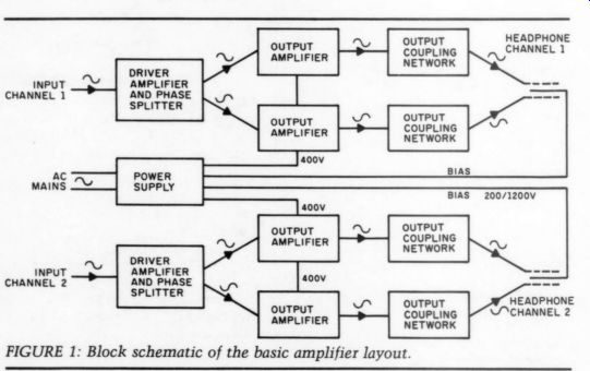
FIGURE 1: Block schematic of the basic amplifier layout.
THIS ARTICLE DESCRIBES a solid-state, high-voltage amplifier for electro static transducers. It contains few parts, has a simple power supply arrangement, and demonstrates high performance. The amplifier is suitable for driving most electrostatic headphones, as well as electrostatic midrange and tweeter units for loudspeakers. It also includes a simple free-field correction filter.
Electrostatic headphones can provide the highest quality sound reproduction.
A drawback, however, is the high volt age needed for drive and bias. Most electrostatic headphones require a driving voltage (AC) of approximately 200 400V across the electrodes. They also need a polarization voltage (DC) in the order of 200V-1kV. For a long time, these voltages needed special circuit considerations to accept transistors with much lower voltage ratings since high voltage transistors were sparse and expensive.
The advent of power supplies, using primary switching (at the “live ” end ahead of the power transformer), has in creased the need for high-voltage transistors and has made it possible to buy suitable inexpensive ones for high-volt age audio amplifiers. On the other hand, high-voltage transformers and capacitors used in vacuum tube amplifiers are scarcer and more expensive.
However, all parts for this amplifier are standard and readily available in electronics supply stores.
To eliminate high-value inductance networks, this amplifier uses a gyrator circuit, simulating a high-value inductance, in its filter. For simplicity and ...
---------------------
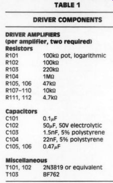
TABLE 1
DRIVER COMPONENTS DRIVER AMPLIFIERS (per amplifier, two required)
Resistors R101 R102 R103 R104 R105, 106 R107-110 R111, 112 100k-ohm pot, logarithmic 100k-ohm 220k 1M-OHM 47k 10k-ohm 4.7k-ohm Capacitors C10 C102 C103 c104 C105, 106 , 0.1uF 50uF, 50V electrolytic 1.5nF, 5% polystyrene 22nF, 5% polystyrene, 0.47uF Miscellaneous T7101, 102 2N3819 or equivalent T103 BF762
----------------
...to keep costs down, the circuit uses only a single power supply. All amplifier stages are of the Class A type. Field effect transistors are used where high impedance and biasing requirements are simplified. The output-stage/high voltage amplifier has a new, effective circuit that minimizes power dissipation and voltage requirements on the transistors. The amplifier has two differential output amplifier stages driving four high-voltage amplifiers to provide the voltages required by the head phones (Fig. 1).
The Differential Driver
The driver amplifiers use three transistors per channel as shown in Fig. 2. Transistor T101, a field-effect type, has simple biasing requirements and high ...
---------------------
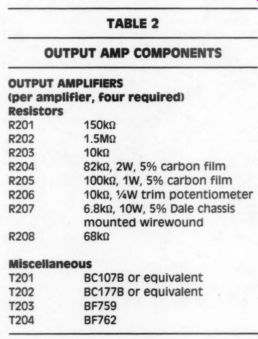
TABLE 2 OUTPUT AMP COMPONENTS OUTPUT AMPLIFIERS (per amplifier, four required)
Resistors R201 R202 R203 R204 R205 R206 R207 150k-ohm 1.5M-OHM
10k-ohm
82 k-ohm, 2W, 5% carbon film
100 k-ohm, 1W, 5% carbon film
10 k-ohm, ¼ W trim potentiometer
6.8k ohm, 10W, 5% Dale chassis mounted wirewound
R208 68k
Miscellaneous
T201 BC107B or equivalent
T202 BC177B or equivalent
T203 BF759 T204 BF762
-----------------
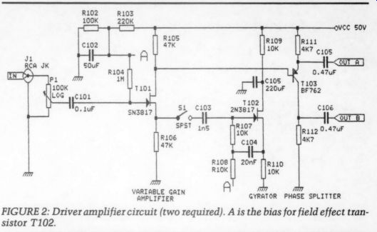
FIGURE 2: Driver amplifier circuit (two required). A is the bias for field effect transistor T102.
-----------------------
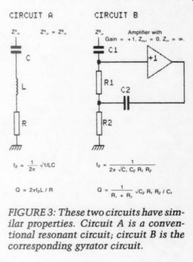
FIGURE 3: These two circuits have similar properties. Circuit A is a conventional resonant circuit; circuit B is the corresponding gyrator circuit.
------------------
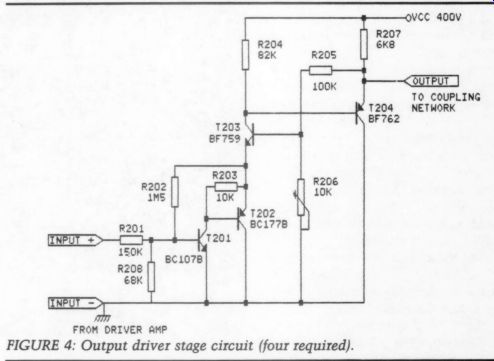
FIGURE 4: Output driver stage circuit (four required).
-------------------
... input impedance. It works as a variable gain amplifier. The gain is controlled by the ratio between the source and drain resistors, equal resistors giving a gain of -1 at the drain. Using a frequency dependent network in either circuit makes the gain frequency dependent.
For example, a series resonant circuit in the source circuit will produce a circuit with a gain peak at the resonance frequency. The gain is controlled by the resonant circuit's Q, which is deter mined by the losses in the inductor and capacitor or by the resistor's series resistance as shown in Fig. 3. However, the high impedances involved make conventional coils extremely large.
This application, for example, calls for a series resonant circuit with a resonance frequency of around 4kHz and a ...
----------------
Performance of the Prototype Unit
Frequency Response at amplifier outputs: +0 - 1dB, 20Hz-20kHz.
Noise and hum: Noise level is approximately - 87dB at 100V (un-weighed).
Hum is approximately -73dB at 100V (A-weighed).
Harmonic distortion (using an HP spectrum analyzer):
At 100V: 100Hz, 0.0003%; 1kHz, 0.003%; 10kHz, 0.003%.
At 10V: 100Hz below 0.0001%; 1kHz, 0.003%; 10kHz, 0.0008%.
The frequency response with the free-field correction filter switched into the circuit is shown in Fig. 8.
-------------------------
...series resistance of around 47k ohm, to give an amplification peak of about 6dB at the resonant frequency.
To avoid the inconvenience of your winding a large coil, this amplifier uses a gyrator circuit. It has the property of transferring the impedance of a resistance/capacitance network into an equivalent resistance/inductance net work as indicated in Fig. 3. If the AC voltages are not too high, the circuit will behave linearly, making a simulated inductance with extremely high value and very low losses possible.
Be careful with active circuits that have resonant elements with high Q values. The voltages in resonant circuits may become very high if the frequency applied corresponds to the resonant frequency of the network. In this application, however, the value of Q is low and the AC voltage applied to the coil at maximum output is only a few volts and in the linear operating region of field effect transistor T102, as shown in Fig. 2. To have a series resonant circuit, include a series capacitance. Using the switch gives you a frequency linear amplifier or one with a frequency correction applied.
Since the output stages require two identical signals 180° out of phase, the driver stage must include a phase split ter. This circuit uses the simplest one; it is a duplication of the input stage. If the emitter and collector resistors of transistor T103 are of equal value and the amplification factor of the transistor is high, the output voltages at the emitter and collector will be almost similar, but 180° out of phase.
Other phase inverter circuits, such as the “long-tailed ” pair, have more sym metrical properties, particularly at high frequencies. In this frequency range, however, the circuit has good proper ties. Because of the DC voltage offsets, blocking capacitors must be used ahead of the output stages. Since the output amplifiers have a high input impedance, these capacitors may be rather small. Do not use electrolytic capacitors since the leakage in them may off set the operating conditions of the output stages.
The High-Voltage Output Stages
The output amplifiers use two sub-circuits, with local feedback around each.
The input circuits consist of transistors T201 and T202 (Fig. 4), which amplify the signal ten times. This amplification is determined by the ratio between resistors R201 and R202. R202 connects to the emitter of T202. Bootstrapping transistor T201 by connecting the collector resistor of this transistor to the emitter of T202 linearizes the operating conditions of T201.
The output subcircuit consists of transistors T203 and T204. The former operates in the common base mode, ...
------------
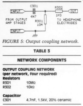
Fig 5
TABLE 3--NETWORK COMPONENTS
OUTPUT COUPLING NETWORK (per network, four required) Resistors R301 R302 10M-OHM 10k-ohm; Capacitor: C301 4.7nF, 1.5kV, 20% ceramic
-------
...which gives high gain and good high frequency response, but low input impedance and high output impedance.
To linearize this stage and raise the in put impedance so the input subcircuit is not loaded heavily, apply negative feedback to the base of T203.
To avoid loading of this transistor's collector, use an emitter follower, transistor T204; it lowers the output impedance considerably so the capacitive loading of the headphones does not affect the amplifier. You can adjust the amplifiers for symmetrical clipping by adjusting the trimmer, R206, since variations in power supply voltage due to variation between transformers used may be quite large. Together, these two subcircuits offer an amplifier with a high input impedance, a gain of around 400 times, low output impedance, wide frequency response, and low distortion. You can adjust the power consumption of the amplifier stages by changing R207; in creasing its value to 15k-ohm will not change circuit performance appreciably.
-------------
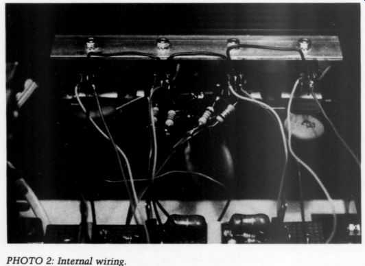
PHOTO 2: Internal wiring.
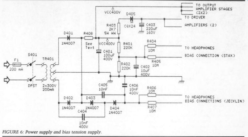
FIGURE 6: Power supply and bias tension supply.
The Output-Coupling Network
To avoid a DC component in the out put voltage, use a capacitor/resistor network to decouple each output amplifier's DC voltage. By using a suitably large capacitor, C301, you can make the attenuation small. The capacitance should be at least ten times that of the headphone (of the order of a few hundred picofarads). Resistor R301 keeps DC voltage to zero. To avoid capacitive loading of the amplifier, you can also insert a series resistance, R302. This resistance, in combination with the capacitance of the headphone, limits the high-frequency response.
You can set this limit safely above the limits of human hearing. If you use the amplifier with electrostatic speakers, these components may be used as dividing network components, although it is preferable to use dividing networks ahead of the amplifiers. If you use one box and a common power supply, this may still be an economical proposition since the amplifiers are simple enough that having separate amplifiers for each element will be rather inexpensive.
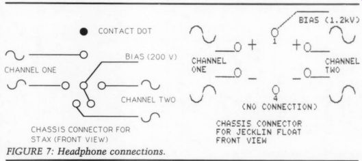
FIGURE 7: Headphone connections.
The Power Supply
You can make the basic power supply simple by using a transformer with a split secondary winding, two rectifiers, and a capacitor as shown in Fig. 6. The balancing action of the headphone elements' push/pull drive makes the unit very tolerant of power supply ripple.
The driver stages operate at a much lower voltage than the output amplifiers and a series dropping resistor is used to obtain the voltage necessary for the drivers (50V). You can add an LED in series with the resistor as a power on indicator.
------------------
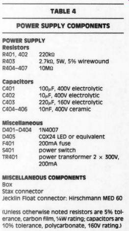
TABLE 4 POWER SUPPLY COMPONENTS POWER SUPPLY
Resistors
R401, 402 R403 RA04-407 220k-ohm 2.7k ohm, 5W, 5% wirewound 10M-ohm
Capacitors
C402 C403 C404-406 100uF, 400V electrolytic 10uF, 400V electrolytic 220 uF, 160V electrolytic 10nF, 400V ceramic
Miscellaneous D401-D404 1N4007 D405 CQX24
LED or equivalent Fa01 200mA fuse S401 power switch
TR401 power transformer 2 x 300V, 200mA
MISCELLANEOUS COMPONENTS
Box Stax connector
-------------------------
Jecklin Float connector: Hirschmann MED 60 (Unless otherwise noted resistors are 5% tolerance, carbon film, 1/2W rating; capacitors are 10% tolerance, polycarbonate, 160V rating.)
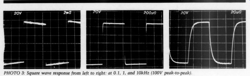
Photo 3
Under no circumstances should you allow the supply voltage to the output amplifiers to be higher than 400V. If your transformer gives a higher supply voltage, insert a series resistor (R408) as shown in the circuit diagram so the voltage drops to 400V. If you cannot find a transformer with the recommended current rating, use one that has a lower rating by increasing the value of the emitter resistors R207 of transistors T204.
Connectors and Bias
The Stax headphones use a Japanese type five-pin connector, whereas the Jecklin Float uses a European six-pin connector. The appropriate connections are shown in Fig 7. It is advantageous to use a Japanese connector, since you do not need to replace the connector at the headphone cable.
Note that the Stax and Jecklin Float headphones have different bias tension requirements. The Stax SR-34 and SR Lambda headphones use about 230V, but the Jecklin Float uses 1.2kV. If you choose the European connector, use one pin (#1) exclusively for the 1.2kV voltage bias and one (#4) for the 230V voltage bias. Some modern Stax head phones, the Stax SR-Lambda Pro and Signature models, use a higher bias voltage (580V). The Stax SR-84 is an electret model and consequently does not need any polarization voltage.
The bias supply for the Stax SR-34 and SR-Lambda is a simple voltage divider, but the Jecklin Float 1.2kV sup ply is a voltage multiplier. Both require a high value of resistance (about 10M ohm) in series with the headphone diaphragm connector to obtain constant charge operation of the headphones.
Amp Construction
You can build the amplifier with ordinary construction techniques. Keep in mind that the voltages involved in the circuits are lethal, so do not make adjustments with power applied to the amplifier. Always allow power supply capacitors to discharge after switching off the amplifier as well.
Follow the recommended voltage and power ratings of the components as specified in Table 1. The prototype amplifier was built using an experimental board, but you can use almost any construction technique (Vero-board or PC board, for example). The output transistors, T204, and mounting tabs of the emitter resistors, R207, are at ground potential so no special insulator is needed; just add heat transfer compound or silicon grease between the tab and the chassis or heatsink. The output stages of one complete stereo amplifier dissipate about 20W.
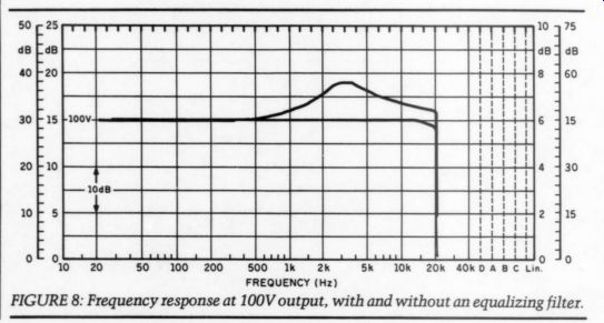
FIGURE 8: Frequency response at 100V output, with and without an equalizing filter.
ACKNOWLEDGMENT
I thank lab technician Mr. Borje Wijk, who assisted in the practical work of building the prototype amplifier.
++++++++++++++++
Also see: