MOSFET MOD FOR THE DYNA ST-120
BY KEN MILLER
DYNACO INTRODUCED the ST-120 in the mid 1960s, it be came one of the most popular solid-state amplifiers of all time. The ST-120 incorporated several design features which remain unique even today and it had the best power supply of any Dyna equipment at the time. Although there are plenty of these amplifiers still around, you don't see them much in audiophile systems. There are a couple of reasons for this. First, a lot of the units need re pair and, second, the sonic characteristics of this amp just don't measure up to today's expectations.
Even in its day, the 120 never drew rave reviews as did Dyna's tube equipment. I attribute all of the deficiencies of the original to the limited solid state technology of the times. The output stage in this amp consists of a pair of NPN transistors in series. This “totem pole” pair is driven by a NPN-PNP pair, forming a quasi-complementary circuit.
This, in turn, was driven by a single ended transistor with bootstrap feed back. The resulting circuitry is non-symmetrical and complex.
Having tinkered with this amp for years and unable to make dramatic improvements to its sound qualities with just minor, on-board parts changes, I became convinced that only totally re-designed circuitry could solve this amp's problems. However, I wasn't sure I wanted to put so much effort into an ST-120. After all, what I really wanted was a good, second amplifier for bi-amping my speaker system, and I thought seriously about buying a new one just for that purpose. I finally decided to do a re-design because I already had one and it met my power requirements. I also like its compact size. Now that my project is finished, I am sure I made the right decision. Audiophiles in various parts of the country favorably auditioned my modified ST-120. It has held its own when compared to some very expensive amplifiers. I think it has a neutral, transparent quality and precise stereo imaging. Violins are silky smooth and transients handled without smearing.
---------------
ABOUT THE AUTHOR
Kenneth P. Miller's interest in audio dates back to the early 1960s. When he is not working at the Health Physics Department at the Callaway Nuclear plant near Fulton, Missouri, he builds preamps, power amps, crossovers, and full-range speaker systems. Other interests include woodworking, canoeing, fishing, and alternative energy.
--------------
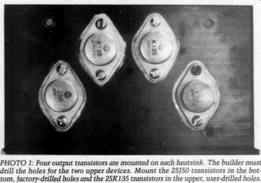
PHOTO 1: Four output transistors are mounted on each heatsink. The builder must drill the holes for the two upper devices. Mount the 2Sj50 transistors in the bottom, factory-drilled holes and the 2SK 135 transistors in the upper, user-drilled holes.
-------------------
In any case, all agree it is a “very listenable ” amplifier with remarkable capabilities considering the parts investment of about $100. Not bad for a 60W/ channel amp with a regulated power supply, complementary MOSFET out put transistors, push/pull drivers, cascode front end, and a JFET input. So if you are looking for an inexpensive way to add a second amplifier to your sys tem, or just want a super upgrade for an existing ST-120, this article is for you. If you don't own an ST-120, plenty of them are still around, many because they need repair. If you buy such, the amplifier portion need not work but the power supply should be operational.
Basically, my modification consists of removing the stock amplifier circuit boards and associated wiring, stuffing new PC boards, (Figs. 4 and 5) and wiring the new ones to the output transistors and power supply. Except for a resistor change, the power supply is used as is.
Design Goals
Once I start a project, I like to finish it in a reasonable amount of time. I ...
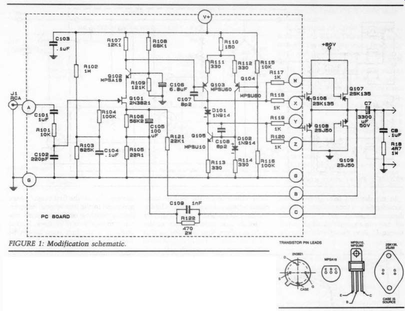
FIGURE 1: Modification schematic.
... dread ordering parts from Timbuktu and waiting eighteen months to get them. I have made every effort to de sign the circuitry using readily available parts. Several circuit areas require high quality parts but these, too, are easy to get. Except for the output transistors, all the semiconductors used are quite common. I bought most of the parts, including the MOSFET devices, from Welborne Labs. They always have the parts I need in stock and ship promptly.
Old Colony Sound Lab also can supply the MOSFETs.
Another of my objectives was to keep this amplifier compatible with the PAS/ 3X preamp. Input impedance of the amp remains at 100k, just as before.
A stock ST-120 can deliver only about 60W/channel to 4-ohm loads. My mod increases capability to about 90W/ channel into 4 ohm loads.
Design Philosophy
There are many important specifications to be met in an amplifier, and no single design can enhance all of them simultaneously. Thus the term “no compromise design ” is a misnomer.
Some compromise is always necessary for a successful design. If this were not so, then amplifier design would be an exact science, not an art. And all amplifiers would be designed the same. As I go through the circuit description, I will point out where compromises were made and why.
-----------
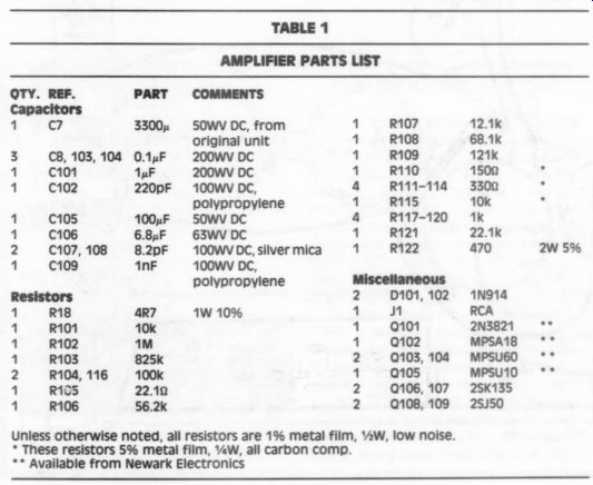
TABLE 1 AMPLIFIER PARTS LIST
QTY. REF.
Capacitors
1 Cc? COMMENTS 50wv DC, from original unit 200WV DC 200WvV DC 100WV DC, polypropylene 50wv DC 63WV DC 3 C8, 103, 104 1 C101 1 C102 C105 C106 C107, 108 C109 100WV DC, polypropylene
Resistors R18 ar? R101 10k R102 1M R103 825k R104, 116 100k RiCS 22.10 R106 56.2k 1W 10% 100WV DC, silver mica R107 R108 R109 R110 1500 R111-114 3300 R115 10k R117-120 1K R121 22.1k R122 470 12.1k 68.1k 121k Ee EF EE EE
:
D101,102 1N914 Nn RCA Q101 2N3821 Q102 MPSA18 Q103,104 MPSU60 Q105 MPSU10 Q106, 107 2SK135 Q108, 109 2SJS0 NNaSN=2aang Unless otherwise noted, all resistors are 1% metal film, 2W, low noise.
* These resistors 5% metal film, “Ww, all carbon comp.
** Available from Newark Electronics
-----------------------
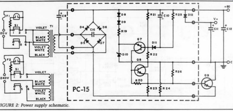
FIGURE 2: Power supply schematic.
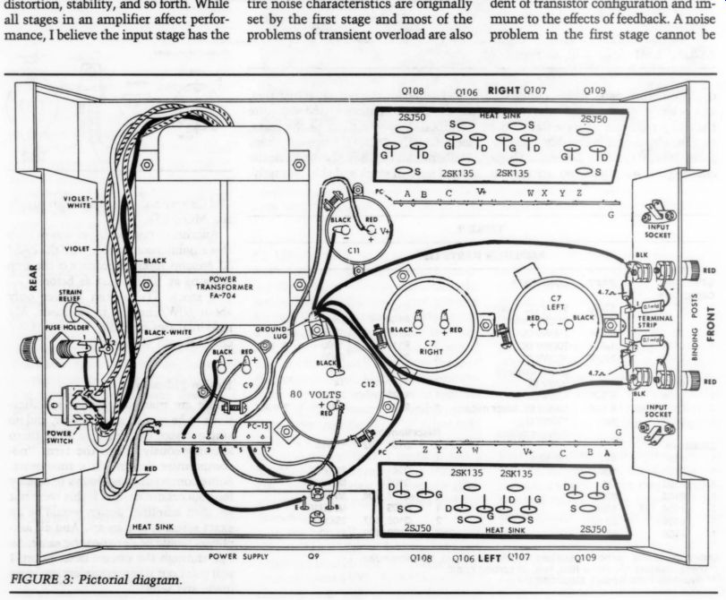
FIGURE 3: Pictorial diagram.
---------------
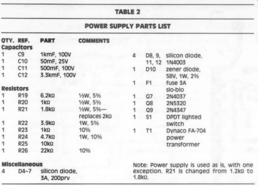
TABLE 2 POWER SUPPLY PARTS LIST QTY. REF.
Capacitors 1 C9 1 c10 1 cn 1 C12
PART COMMENTS
1kmF, 100V 50mF, 25v 500mF, 100V 3.3kmF, 100V silicon diode, 1N4003 zener diode, 58V, 1W, 2% fuse 3A slo-blo 2N4037 2N5320 2N4347 DPDT lighted switch
Dynaco FA-704 power transformer Resistors R19 R20 R21 6.2 k-ohm 1 K-OHM 1.8 k-ohm 0.25 W, 5%
0.5 W, 5% 0.25 W, 5%- replaces 2 k-ohm 0.25 w, 5% 10% W0.25 w, 10%
R22 R23 R24 R25 R26 3.9k0 1 k-ohm 4.7 k-ohm 10 k-ohm 22 k-ohm 10%
Note: Power supply is used as is, with one exception. R21 is changed from 1.2 k-ohm to 1.8 k-ohm.
Miscellaneous 4 D4-7 silicon diode, 3A, 200prv
-----------------
In my design I have given careful consideration to the problems of noise, distortion, stability, and so forth. While all stages in an amplifier affect performance, I believe the input stage has the most influence on the overall sonic characteristics of an amplifier. The en tire noise characteristics are originally set by the first stage and most of the problems of transient overload are also associated with the first stage! Noise generated in the first stage is independent of transistor configuration and immune to the effects of feedback. A noise problem in the first stage cannot be “fixed ” in later stages. Thus I begin any amplifier design with the input stage.
The Circuit
Refer to Fig. 1, transistors Q101 and Q102 form the input stage, a cascode arrangement for wide bandwidth. Q101 is a 2N3821 JFET transistor. Had I used a bipolar here, I could have achieved a slightly better noise figure for the amp.
However, the JFET is much more resistant to overload and does almost as well as a bipolar in the noise category.
C101 couples the incoming signal to the first stage.
R101-C102 form an input low-pass filter. R102-R103 form a DC bias net work for Q101. C104 is a noise shunt.
R105-R106 in the source circuit of Q101 are part of its bias network. C105 is a noise shunting capacitor. R108 R109 form the bias network for Q102, with C106 a noise shunt. R107 is the collector load resistor for Q102. Transistors Q103-Q104 form a differential pair. R115-R116 provide forward bias on Q104. R110 is a constant current source for the differential pair. R111 R112 supply degenerative or local feed back to the pair, eliminating the need for a matched pair. Q104-Q105 form a current-mirror.
The output of Q104 is developed across D102-R114. This network is essentially the same as the one formed by R113 and the base-emitter junction of Q105. Thus Q105 is forced to follow Q104. Q103-Q105 work push/pull to deliver a signal to the output transistors. C107/C108 are the phase lag compensating capacitors for stability. Transistors Q106-Q109 are paralleled, complementary transistors in the source follower configuration. C7, C8, and R18 are parts in the chassis re-used in my design. C7 is the output coupling capacitor. R18-C8 form a phase correcting network.
R121 provides both AC and DC feed back to the source terminal of Q101.
It holds the source terminals of the out put transistors to one-half the power supply voltage. R122 is the main AC feedback resistor. The combination of R105 and R122 set the overall voltage gain of the amplifier at about 20, or 26dB. C109-R122 form a low-pass filter and this network, along with the input stage low-pass filter, roll off the high frequencies at an effective rate of 12dB/ octave. This mirror minimizes slew induced distortion.
I believe MOSFET devices for the out put stage are a better choice than bipolar transistors because of their better thermal stability. They do require a higher drive voltage and this is accomplished by raising the power supply voltage from 72-80V DC. This voltage change is made by replacing one resistor in the power supply regulator board.
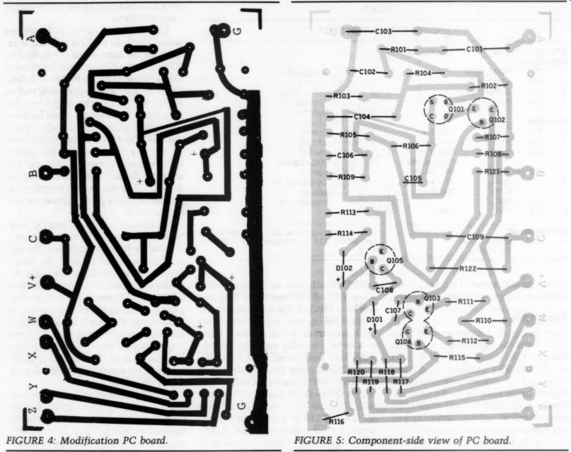
FIGURE 4: Modification PC board. FIGURE 5: Component-side view of PC board.
A schematic diagram and parts list for the power supply is shown in Fig. 2. Since the power supply is left “stock, ”' it won't be discussed here. Figure 2 is just for troubleshooting purposes.
Amplifier sensitivity is 1.1V RMS at 1kHz for 60W out into 8-ohm. Distortion figures are typically less than 0.2% THD at 60W output at any frequency in the audio spectrum. The internal slew rate is too high for me to measure accurately with my equipment; it computes out to 75V/microsecond. Operating slew rate is about 10V/microsecond. The one-half power points are 6Hz and 70kHz.
Construction Tips
You will be wise to read this entire section before beginning any work on the chassis.
While waiting for parts to arrive, you can do several things to prepare the unit for modification. Remove the original PC boards (marked PC-14), heatsinks, and associated wiring. Since the original power supply and regulator board (PC-15) will be re-used, leave that portion of the amplifier intact. Also, don't remove the 4.7-ohm resistor/ 1uF capacitor assembly. I suggest using a pair of diagonal cutters to just snip off wires until the chassis looks like the one in the pictorial diagram (Fig. 3.) Next, remove the amplifier heatsink/PC board assemblies. If your chassis needs cleaning, this is the time to do it.
When the chassis is clean, add a ground wire to each input phono jack.
You should solder these two wires together at the chassis ground lug at one end, and to the “cold ” or chassis terminal of the input jacks at the other end. They should be routed alongside the other ground wires going to the speaker jacks. You will need to add an other ground lug on top of the existing one in order to accommodate all the additional ground leads. Again, this is a good time to do it because there is plenty of working space inside the chassis.
The ground wires which you have just added (as well as all the additional wiring to be done) are not shown in the pictorial diagram. The pictorial is sup plied as an aid in locating the major components in the unit as well as de fining the locations right, left, front, and rear.
On the existing power supply regulator board (PC-15), connect and solder the wire from terminal 5 to the + (red) terminal of C11. This terminal is marked V + on both the schematic and pictorial diagrams and is shown on the pictorial.
Now test the power supply, with proper temporary loads in order to obtain the correct voltage readings. Temporarily solder a 500 ohm, 10W resistor across C12. If you haven't such a resistor handy, remove the two 300 ohm, 7W resistors from one of the PC-14 circuit boards, connected in series to form a 600 ohm load.
With the power supply loaded, turn on the unit. The DC voltage across C11 and C12 should read about 72V if the power supply is working properly.
Once you are satisfied it is okay, turn off the power and unplug it.
Next, remove PC-15 from the heat sink. Locate the 1.2 k-ohm resistor (brown red-red) near the middle of the board.
Remove this and replace it with a 1.8 k-ohm, AW resistor. With a little care and patience, you can make this resistor change without disconnecting any of the wires attached to PC-15. Remount PC-15 on the heatsink. Turn on the unit and again read the voltage across C11 and C12. This voltage should now read about 80V DC. If so, unplug the ST-120 and remove the load resistor, being sure the caps are fully discharged. The power supply alteration is complete.
In the interest of safety replace the original power cord with a three-prong grounded type. The green lead should be soldered to a lug mounted under one of the transformer mounting bolts.
Next, prepare the two heatsinks removed earlier from the chassis. Since four TO-3 style power transistors must be mounted on each sink, and since the originals are drilled for a single pair, you must locate and drill holes for the second pair. Their location is not critical.
Refer to Photo 1 to see where I located mine. A mica insulating wafer makes a nice template. Before you drill the holes be sure they are oriented like the factory-drilled holes. Otherwise the gate and drain pins will be reversed when compared with the pictorial dia gram. It is very important the holes you drill are burr free on both sides of the heatsink.
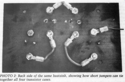
Mount the 2SJ50 transistors on the heatsinks using the bottom, factory drilled holes. Mount the 2SK135 transistors in the holes you drilled. You will need an additional eight nylon bushings like the ones Dyna supplied for the original transistors. I recommend you fasten each transistor to the heatsink using 0.75 ” x 6-32 screws. That way, you can attach the cases together using jumpers, just as I did. The case of the transistor is the source terminal and all four cases must be tied together, Photo 2. 1 used short pieces of #14 wire with a ring terminal soldered at each end.
Then slip each ring terminal over a mounting screw and tighten it with a second hex nut.
In Photo 2, the wire running out to the side is the lead which attaches to C7. This wire is also attached to a mounting screw as the jumpers. Make this lead from a 12” wire that was originally wrapped around C7. You will need two of these-one for each heat sink, with a ring terminal soldered to one end of each. On one heatsink at tach the terminal end of this wire to the upper mounting screw of the 2SJ50 transistor on the left half of the sink.
On the other heatsink, fasten the other 12-inch length to the upper mounting screw of the right side 25J50. Cut four 16-inch lengths of a red #18 wire and four black ones to the same length.
Cut eight 8-inch lengths of a #22 wire-four red, four black. Also, remove a 6-inch length of insulation from a #18 wire and cut it into sixteen 1/4-inch pieces. Slip one of these insulating sleeves over each gate and drain pin and push them down as far as they will go.
Solder one end of each #18 red wire to the drain pin of each 2SK135. Do the same with the black wires to the 2S]50 transistors. Solder one end of the #22 red wires to the gate pin of each 2SK135.
Solder the four remaining #22 black wires to the gate pin of each 25j50. Set aside the heatsinks.
Nothing has been said so far about special precautions when handling the MOSFET devices. These particular units have internal diodes across the terminals to protect against excessive voltage. I have handled literally dozens of these units as if they were bipolars and have not had a single failure. So I don't believe any special precautions are necessary.
------------------
After your PC boards are stuffed and soldered, visually inspect each one for poor solder joints. Are the diodes and capacitors installed with the correct polarity? Q101 has a small tab on the case which should be pointing downward toward the heavy ground trace on the foil side of the board. Cut twelve 12 ” lengths of #22 wire.
On each board solder one end of a wire to eyelets A, B, C, V+, and either eyelet G. You are going to test each PC board under power, one board at a time.
Find the free end of the eyelet A wire and temporarily solder it to the ground trace on the foil side of the board. The free end of the eyelet G wire gets soldered to a chassis ground. Solder the eyelet C wire to the negative post on C7. Solder eyelet V+ wire to the plus terminal of C11. Temporarily solder one end of another piece of 12 ” wire to the + end of D101, and the other along with the free end of eyelet B wire, to the + (red) terminal of C7.
Position the board so it is lying foil side up outside of and not touching the chassis. The board should be resting on dry wood or other non-conducting surface. Apply power to the unit. With a VOM set to the positive DC function, connect the negative meter lead to eyelet Z and the positive meter lead to eyelet W. The meter should read 0.5-0.75V DC. Now place the negative meter probe on eyelet Y and the other probe on eyelet X. The meter should read the same as before. Set the meter to 100V scale and read the voltage between chassis ground and the positive terminal of C7. This should read 35-45V DC.
----------
SOURCES
Newark Electronics 4801 N. Ravenswood Ave. Chicago, IL 60640-4496 (312) 784-5100 FAX (312) 784-5100, Ext. 3107
Newark Electronics International 1625 Trinity Dr. Mississauga, Ont. Canada L5T 1W9 (416) 670-4185, FAX (416) 670-4187
Welborne Labs, 6836 S. University Blvd. #70 Littleton, CO 80122, (303) 470-6585
---------------
---------------
REFERENCES
1. Motchenbacher and Fitchen, Low-Noise Electronic Design, John Wiley and Sons, New York, 1973.
2. Jung, Walter G., Audio IC Op-Amp Applications, Howard W. Sams & Company, 3rd edition, 3rd printing, 1988.
----------------
Turn off the power and remove the PC board from this test setup by unsoldering the leads from the chassis connections. Leave the other ends of the wires soldered to the eyelets. Unsolder the end of the eyelet A wire which was soldered to the ground foil. Completely remove the jumper between D101 and C7. Test the second PC board in similar fashion. A board which will yield volt ages under test other than those in the above parts graph is defective and should not be connected to the output transistors until it passes the test. Doing so can result in a needless, expensive re placement of the power MOSFETs.
Be sure the unit's power [and caps discharged] is off before continuing. At tach each PC board to a heatsink using only two spacers per assembly. Mount them in the bottom pair of holes. At tach the screws loosely for now. Check each module for correct mechanical assembly. The foil side of the PC board should be facing the pin side of the out put transistors. The heatsink mounting flange should be downward and facing out. The letters designating various eyelets should be visible from the top of the assembly. The long mounting screw heads should be against the heat sink while the nuts tighten up against the PC board.
Place each assembly in position on the chassis and securely tighten the sink flange to the chassis. Bend back the phono jack terminals if they touch any component on the PC board. Care fully route the wires to their intended terminations. All #18 black wires from the drains of the 2SJ50 transistors are soldered to the chassis ground lug. All #18 red wires from the drains of the 2SK135 transistors are soldered to the + 80V lug on C12. The solder lug on this capacitor is too small to accept all these leads, so use one of the wires to “'extend ” the terminal.
All wires from the heatsinks and the PC boards are overly long so should be cut to the correct length before solder-ing. Insert the red #22 wires from the gates of the 2SK135s foil side first to eyelets W and X and solder the black gate leads from the 2Sj50 to eyelets Y and Z. Two “G ” eyelets are located near the bottom of each PC board. One, and only one, of these should be connected to the chassis or “cold ” input jack terminal. Use whichever one is closest to the phono jack. The free end of the eyelet A wire goes to the 'hot' terminal of the input jack.
The wire from the sources goes to the + terminal of C7 along with the wire from eyelet B. A wire from the red output speaker jack goes to the negative side of C7 along with the wire from eyelet C. The wire from eyelet V + goes to the positive terminal of C11. Neatly tie wrap the bundles of wires going to chassis ground and C12. Inspect each drain and gate pin on the power transistors, be sure none are bent over and touching the heatsink. Install the other two spacers in each board and tighten all four nuts.
Your ST-120 modification is now complete and ready to use.
Using Your 120
A modified ST-120 generates little heat but this still must be dissipated effectively. So don't cover it with record jackets, or other paraphernalia. The amplifier may be used with any speaker sys tem having a rated impedance of 4-ohm or greater. This amp can drive 2 ohm loads at reduced power but the heatsinks are not large enough for low-impedance operation. Prolonged high-frequency, high power testing using sine or square waves can damage the unit. Make such tests quickly and allow the amp to cool be tween tests. The amplifier has no built in protection against a shorted output.
If no sound comes from the amplifier when it is turned on, investigate the cause before turning up the volume (a good idea with any amplifier). Your amplifier should deliver many years of superb sound. Happy listening!
--------------
Also see: