ENCAPSULATED MODULE
HARDLY A NEW idea, electronic circuits packaged in potted modules are a familiar sight. Indeed, modern integrated circuits are the epitome of semiconductor technology applied to ward encapsulation and miniaturization. The following amplifier construction technique, which is especially suited for the amateur prototypist, is based on using potted amplifier modules in epoxy-filled cases. These are then plugged or soldered into a main circuit board universally wired as a preamplifier.
In addition, I'll describe a built-in preamplifier circuit that is low enough in all forms of distortion to be considered audibly perfect. I'll show you how I characterized its performance, and the measurement techniques I used to back up this claim.
To make an encapsulated module, load, wire, and solder a small circuit board and then place in a suitable en closure, of plastic, ceramic, or metal construction. Then, pour a potting com pound into the enclosure and allow the entire assembly to cure in ambient conditions. Sometimes I evacuate the assembly immediately after pouring to re move potential voids left by air bubbles, then cure it at elevated temperatures to accelerate the process. Figure 1 illustrates this construction. The resultant module is one solid brick of thermally conductive composite materials and components with high dielectric strength.
--------------
ABOUT THE AUTHOR
John Adelsbach graduated in 1970 with a BSME from Cal Poly. After a stint at Westinghouse Electric, he returned to school and was awarded a M.E. from Cal Poly in 1976.
He then joined Hewlett-Packard, working on plotters, disk drives, PCs, and terminals. He currently is the program manager for the HP 800 and 900 series of client/server workstations. Other interests include video, software writing, and long distance running.
-----------------
Hardwired, 3-D component mounting; Plastic; Metal; Ceramic; Perforated Board
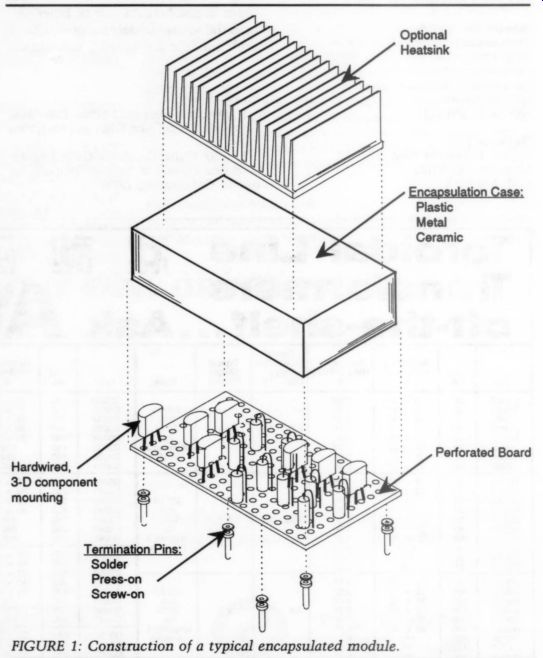
FIGURE 1: Construction of a typical encapsulated module.
----------------------
Benefits
Key benefits to applying this technique are:
Simplicity. You can construct all module circuits on standard perforated prototyping boards and lay out components “on-the-fly ” without careful trace path planning. What's more, slip shod workmanship is ultimately hid den (potted) from view. For standard amplifiers, only input, output, power, and ground terminals are required out side the module-other circuit nodes remain internal.
Strength. A completed module is a solid block of hardened epoxy resin which produces low component shock, vibration, and lead stress. Any fragility of the board or components is largely forgiven.
Compact Size. Modules invite high density designs which means ordinary board-layout design rules and spacings don't apply. You can wire circuits in all three dimensions, create “air nodes, ” and solder lead-to-lead without strain relief. As an added benefit, short wiring paths allow for less stray capacitances, higher speed circuits, and greater immunity to noise and hum.
Modular Design. You can swap en tire amplifier circuits without disturbing the main circuit board thereby pre serving a major portion of the labor you invested in prototyping preamps. The interconnect wiring, switches, controls, and mechanical parts remain untouched $0 you can compare alternative amplifier designs quickly and easily.
Isothermal. All components within a module are held at a constant relative temperature. The entire module acts as a heatsink and minimizes operating point drift caused by local heating. It also improves the circuit's ability to cool due to the larger surface area. If necessary, you can apply external heat sinks to modules as well.
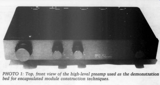
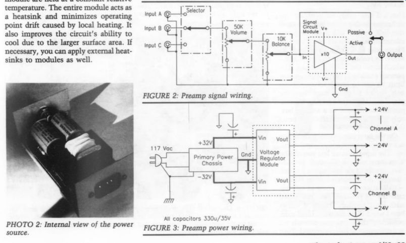
PHOTO 2: Internal view of the power source. Photo 3; FIGURE 2.; FIGURE 3: Preamp power wiring.
Limitations
Two potential drawbacks to employing encapsulated modules are:
Thermal limitations. Each module has a finite thermal capacity dictated by its surface area. Just as there is a thermal gradient in a transistor from junction to case, the module components' temperature will be higher than the case surface, depending upon the potting compound's thermal conduction. Most compounds have good thermal conductivity, but they do vary.
The compounds intended for electrical applications have linear thermal-expansion coefficients similar to that of semi conductor packages. (Indeed, some pot ting compounds are made from the same materials used in making transistor and IC packages.) Service limitations. Because the smallest replaceable unit is the module itself, its components cannot be individually replaced for repair or adjustment. Once potted, it is sealed for life.
Designing Out Limitations
To overcome these drawbacks, I used only conductive electrical-grade epoxy and kept any thermally sensitive components outside the module. Most importantly, modest preamp requirements allowed each module to operate at low power. I don't have any direct workarounds to the service limitations, but I do have some preventative approaches:
------------
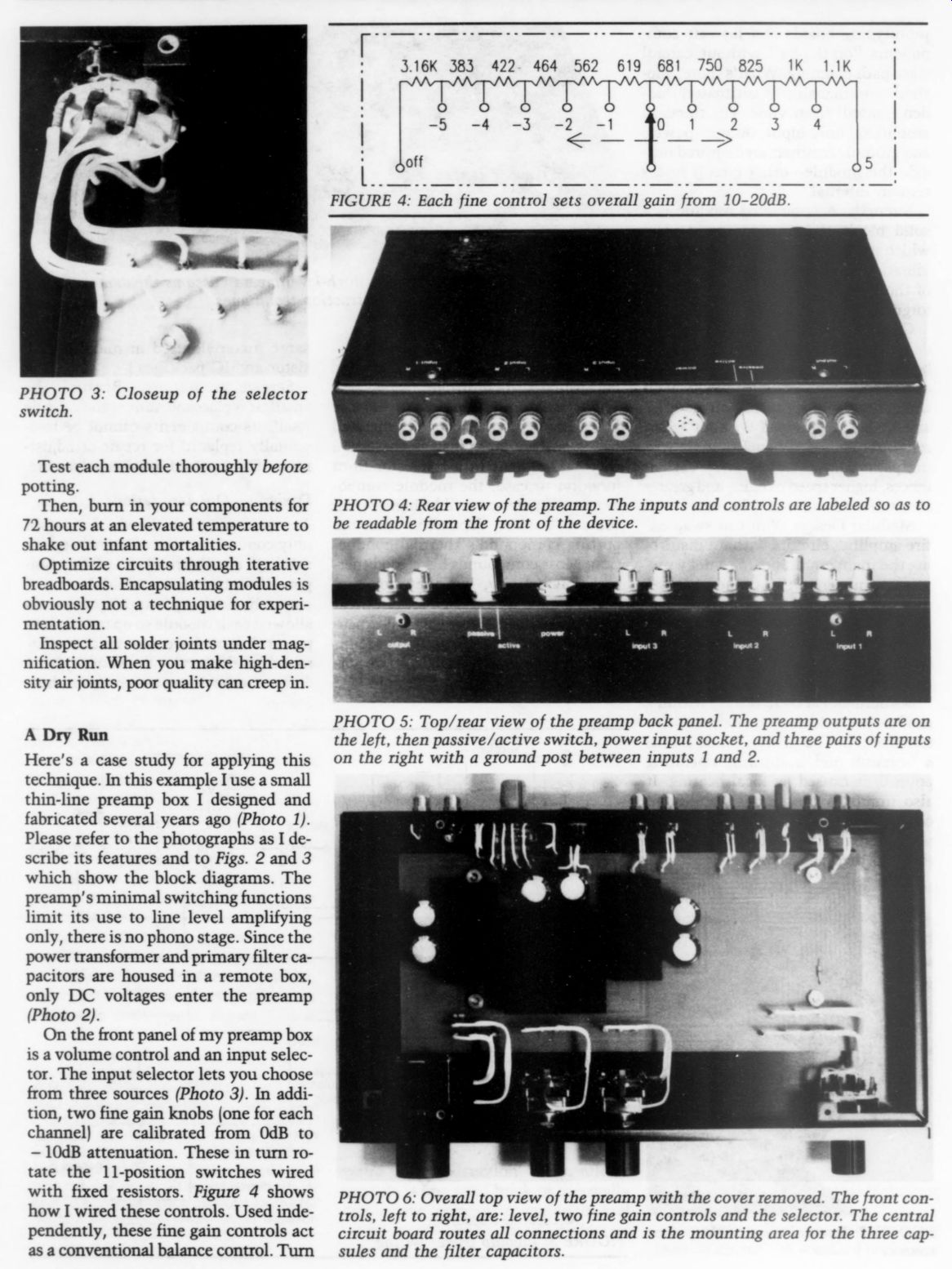
PHOTO 3: Closeup of the selector switch.
Fig.
PHOTO 4: Rear view of the preamp. The inputs and controls are labeled so as to be readable from the front of the device.
PHOTO 5: Top/rear view of the preamp back panel. The preamp outputs are on the left, then passive/active switch, power input socket, and three pairs of inputs on the right with a ground post between inputs 1 and 2.
PHOTO 6: Overall top view of the preamp with the cover removed. The front controls, left to right, are: level, two fine gain controls and the selector. The central circuit board routes all connections and is the mounting area for the three capsules and the filter capacitors.
PHOTO 7: Underside of the circuit board, normally mounted to the removed plate using four standoffs which match the four large empty circuit card holes.
-------------
Test each module thoroughly before potting.
Then, burn in your components for 72 hours at an elevated temperature to shake out infant mortalities.
Optimize circuits through iterative breadboards. Encapsulating modules is obviously not a technique for experimentation.
Inspect all solder joints under magnification. When you make high-density air joints, poor quality can creep in.
A Dry Run
Here's a case study for applying this technique. In this example I use a small thin-line preamp box I designed and fabricated several years ago (Photo 1).
Please refer to the photographs as I describe its features and to Figs. 2 and 3 which show the block diagrams. The preamp's minimal switching functions limit its use to line level amplifying only, there is no phono stage. Since the power transformer and primary filter capacitors are housed in a remote box, only DC voltages enter the preamp (Photo 2).
On the front panel of my preamp box is a volume control and an input selector. The input selector lets you choose from three sources (Photo 3). In addition, two fine gain knobs (one for each channel) are calibrated from 0dB to - 10dB attenuation. These in turn rotate the 11-position switches wired with fixed resistors. Figure 4 shows how I wired these controls. Used independently, these fine gain controls act as a conventional balance control. Turn one up and its channel gets louder. Used jointly, they act to set the overall pre amp gain (or sensitivity). Since the pre source levels. Figure 4 is a schematic of these controls.
Ins and Outs amp gain is 20dB, the fine gain controls adjust the overall gain-between 10dB 20dB, thereby accommodating diverse The preamp's back panel contains three pairs of inputs; a ground lug, the DC power receptacle, the output jacks, and an “active-passive ” switch (Photos 4 and 5). This switch routes the jacks on the back panel to the output from either the amplifier (active), or the out put from only the switches and controls (passive, no gain). Additionally, this switch has allowed me to experiment with comparing the distortion of the active circuit to the “sound ” of just a wire. I'll tell you about the results of these tests below.
Inside the chassis, one main circuit board interconnects wiring to the in puts, outputs, and controls. Three en capsulated modules ( EMs) are mounted on the board (Photo 6). The two smaller modules house the signal amplifier circuitry, one or each channel. The third module holds the active portion of the regulated power supply. Benefitting from the EM approach, I laid out and etched this main PCB only. The EMs use the “grundgy ” prototyping style I've outlined above.
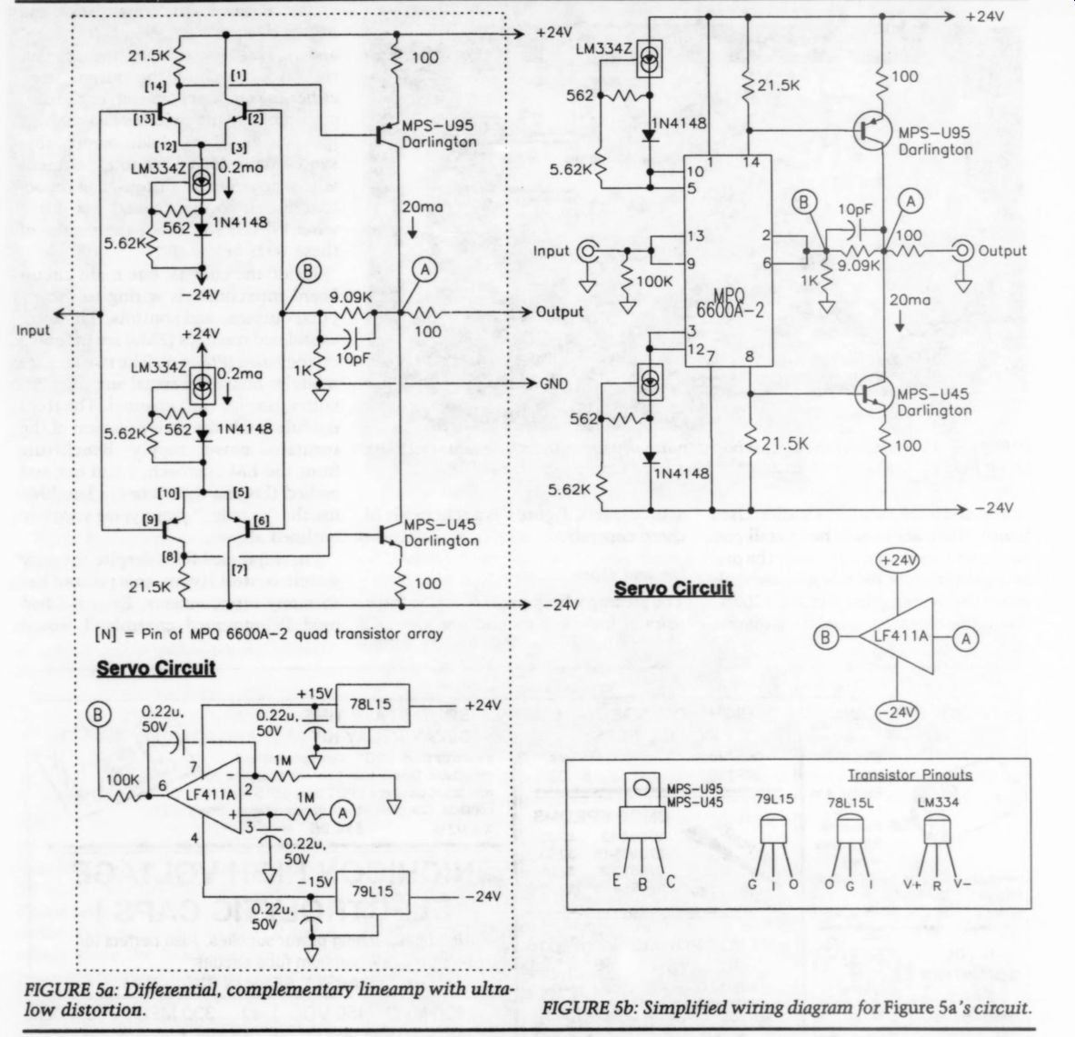
FIGURE 5a: Differential, complementary lineamp with ultra low distortion.
I'm impressed that, despite the very simple control layout, this preamp has so many interconnects. Even if I had used PC-mounted controls, I would have had to make each and every one of these connections. The overall architecture points out what I think is a key benefit of the EM approach.
I don't know about you, but I know I have two reactions to preamp prototyping: I want the ability to easily experiment with different circuits, and I hate to repeat all the tedious interconnect wiring time and again. The EM approach eases these conditions. The control/switching/interconnect structure is done only once. This EM approach al lows me to rapidly and reliably change, experiment, and compare entirely different amplification circuits. You need not even encapsulate the signal circuit boards to enjoy these benefits.
You can build experimental modules then plug them into this preamp “switchbox. ” No more new board lay out and rewiring with each change. If you're like me, you'll want to play around with different types of power supply modules as well.
Construction Highlights
So far, I have built and evaluated three different preamp circuit designs. Since all had the same interconnect design, I built only three sets of amplifier modules, interchanging them in this experimental chassis to measure and listen.
I'll also describe my experiences with three designs of power supply modules.
Inside the chassis are three EMs and all the interconnect wiring. You can attach modules to the main board in three ways. Soldering is the most reliable, although the most time-consuming to disassemble. If you choose pin and socket connectors, use only reliable ones, especially at low currents. Gold plated contacts and gas-tight seals offer real benefits here. Finally, you can use ...
-----------------
TABLE 1 OVERALL PERFORMANCE
Rated Output: 3V rms, 0.1Hz-400kHz
Maximum Output: 16V rms, 20Hz-20kHz
Output Impedance: 100 ohms
Total Harmonic Distortion: Less than 0.0015% @ 1kHz, 3V rms
Frequency Response: +0, -0.1dB, 20Hz-20kHz
Maximum Input Signal: 15V, volume control @ -20dB Gain: 20dB Input Impedance: 8.3k ohms, active or passive Signal-to-Noise, unweighted: Greater than 96dB Output Offset: Less than 0.2mV at any volume control setting Maximum Input Offset: 1V at -20dB volume control setting
Maximum Output Noise: Less than 100uV, unweighted Separation: Greater than 96dB @ 1kHz 96dB @ 10kHz 91dB @ 100kHz Gain Tracking Error: Less than 0.15dB at any volume setting Less than 0.015dB above 12 o'clock Slew Rate: 12 V/u-sec Rise Time: 2.5usec maximum
------------------------
... crew-type terminations which allow for quick assembly and disassembly.
In my favorite method, I press and swage gold-plated, brass pins through the EM-perforated board, then solder module components to that node. After constructing the module, I have five or more input/output connections. In this example, I have V+, V-, ground, signal input, and signal output.
Since most perforated boards have close dimensional accuracy, placing each termination in the same location on each module board will allow all to drop into the same footprint on the main PC board. This makes it easy to fabricate modules that retain dimensional consistency and are therefore interchangeable.
A few other important tips about the construction of the EMs:
Give yourself room. Complex circuits are difficult to wire in a small space. As you gain experience, how ever, you can wire increasingly dense circuits in three-dimensional space. It's like a cubic jigsaw puzzle.
Use the right potting compound.
Many five-minute epoxies absorb too much water. This can be bad news to high impedance points within circuits.
Even megohms of volume resistivity can upset operating points in FET circuits. Also, watch for good thermal conduction properties. Employ appropriate electrical quality compounds.
Use plastic craft boxes for module cases. I bought small clear or colored plastic boxes available at craft stores, then used the bottom section as the cover. After potting, I spray the cover a satin black for a uniform appearance.
You can also use deep-drawn metal cans which are suitable for low-level circuits requiring the high hum and noise immunity offered by a shielded, grounded enclosure.
The Circuit
Of the three circuit designs with which I experimented, I consistently favored the one shown in Figs. 5a and 5b. This is a variant of popular differential, complementary designs I've been seeing over the last ten years. To this topology, I've added some features of my own and applied the circuit to a rigid computer-simulated analysis to optimize its performance. The overall preamp performance is characterized in Table 1.
I admire this circuit's elegance and design simplicity. It contains intrinsic engineering solutions to all performance considerations. It is inherently self-balancing, stable, wide in band width, and it self-cancels nonlinearities. The key to my design's outstanding performance lies in its quad transistor array. This array houses four transistors formed on the same substrate and matched in AC and DC parameters-all on a 14-pin DIP. Applied to this topology, the performance is exemplary. Nearly all nonlinearities are balanced. Its static and dynamic distortion is so low that it is difficult to mea sure on my test equipment.
You may feel free to make parts substitutions, but retain the operating voltage points. Be sure to use the MPQG6600A-2 transistor array, this is critical to performance. While the Darlingtons I used as output drivers have a high current gain, there are equivalent substitutes-both integrated and discrete. The servo circuit adds a little complexity but saves having to add the DC blocking capacitor. If you wish, you can eliminate the servo circuit and add the cap to the output-either way will work fine. The current sources trans late into a bit of overkill, and thermally compensating them is probably not necessary. Use your own discretion.
The Power Supply
Any power supply generating +-24V is appropriate. The circuit in TAA 4/90 is fine.! My shunt regulator in TAA 4/88 also works well, although it re quires a pre-regulator.? I have chosen here a third approach-a dual-tracking regulator shown in Fig. 6. It is supplied by the primary power chassis shown in Fig. 7. This design has very low output impedance, high bandwidth, and high common-mode rejection although transient response is very good. Use low impedance capacitors at the output for the best performance. Use the design equations shown in Fig. 6 to determine output voltage magnitude as well as the current limit shut-down point.
Evaluating Performance
I evaluated the preamp's performance by four means. First, I developed a computer simulation of the circuit comprised of behavioral models of each of the physical components. These characterized both linear and nonlinear behavior as well as thermal and parasitic effects. Playing with component values allowed me to quickly iterate to an optimized circuit. The simulation predicted outstanding performance. Before constructing the circuit, I also deter mined the values of key components to observe the circuit's sensitivity. This gave me an indication of design margins and latitudes of value changes upon performance.
-------------------------
Differential Testing
In this differential test, I compare one channel of the amplifier under test to a straight wire without gain. Figure A is an illustration of the test setup. First, feed a line-level source into an amplifying stage to increase its gain. Commonly, this is the unused channel of the amplifier you are testing. This boosts the signal at the input of the testier to hear and therefore increasing the test sensitivity. Since this booster amplifier is common to both sides of the differential setup, any distortion of the booster amp itself is nulled, and there fore has no effect on the outcome.
Then, reduce the amplifier signal line's gain to that of the wire with a precision passive atten. The signal continues into both the straight line and the active amplifier, and on into the headphones. An important note: The preamp must be able to drive the headphones (or any chosen load) without distortion. Since the head phones respond only to differences in voltage across their speakers, if both lines feeding the headphones are identical, there will be no audible output.
When the active amplifier deviates from perfection (represented by the wire output), it no longer traces the output identically to the straight wire node. The difference between these two signals creates a voltage difference across the headphones, thereby generating a current exactly proportional to the amplifier's sound and volume distortion.
The degree to which the amplified signal deviates from the straight wire signal measures the accuracy and sonic purity of the signal. The sound heard through the headphones is exactly the sound and the amplitude of all inaccuracies that the preamp is producing, generated by all imperfect means, both known and unknown.
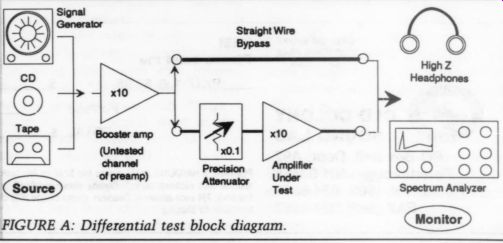
FIGURE A: Differential test block diagram.
This test is a simple approximation of a distortion analyzer, but it has one key advantage. It measures distortion in real time. Unlike a THD meter, the differential tester does not need repetitive waveforms to null the fundamental frequency. This means random signals like music can be used as the source.
Spectrum Analyzer
-------------------------
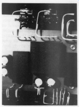
PHOTO 8: Closeup of the encapsulated modules which are, in turn, mounted on the interconnecting mother board. The balance switches are at the top, the left and right “3” inputs, power input and passive/active selector switch are at the bottom.
Next, I built the circuit on a bread board and measured essentially the same performance predicted by the computer model, thereby validating the simulation's integrity. Increasingly over the years, I have gained confidence in this modeling software's ability to predict physical reality. The only discrepancies I usually see result from inaccurate device characteristic assumptions or prototype wiring errors.
SOURCES
Potting Compound Manufacturers Moyen, C.P. Company 8157-T Monticello Skokie, IL 60076 (708) 673-6866 Emerson & Cuming, Inc., A Grace Company 77 Dragon CT Woburn, MA 01888 (617) 935-4850 Hysol Aerospace and Industrial Products Div. The Dexter Corporation Folly Mill Rd. Seabrook, NH 03874 (603) 474-5541 JC Dolph Company PO Box 267
Monmouth Junction, NJ 08852 (201) 329-2333 General Electric Company Silicone Products Division Waterford, NY 12188 (518) 237-3330
-----------------
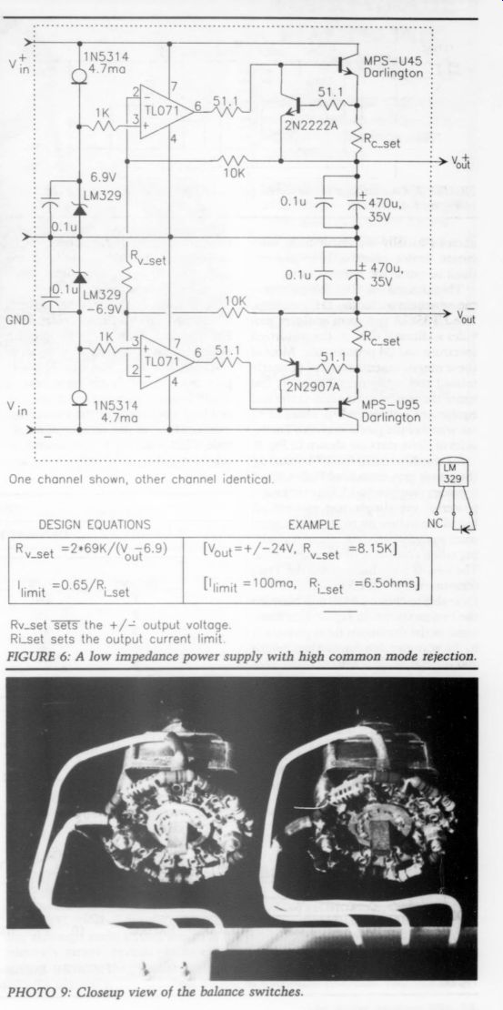
FIGURE 6: A low impedance power supply with high common mode rejection.
PHOTO 9: Closeup view of the balance switches.
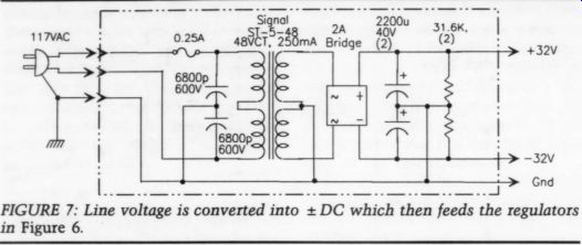
FIGURE 7: Line voltage is converted into + DC which then feeds the regulators in Figure 6.
Then I used an HP339A-distortion measurement set for the THD readings.
The HP3582A spectrum analyzer provides additional data on the distortion spectrum and IM performance. Most of these measurements reached or nearly missed test equipment limits. A few times the readings remained at the test equipment's threshold. (I checked to see whether the power was on!) The results of these tests are shown in Fig. 8.
For the differential tests, I hooked up the circuit into a modified Hafler XL-10 topology (see Sidebar). This strikingly powerful yet simple test method al lowed me to hear (or to see on the spectrum analyzer) what the circuit was adding when compared to a straight wire.
The results were higher than the THD measurements but no less impressive.
I was able to obtain a 84dB null between the two as shown in Fig. 9. I attribute some of the deviations from perfection to the wire circuit's limited bandwidth and the test setup sensitivity, not only to errors in the amplifier. These limitations are due to cable-capacitance frequency rolloff and measurement equipment input impedance.
Be assured, however, that the level of distortion in this circuit is inaudible.
For example, if you were to play this preamp in an extremely quiet room of 35dB ambient level, you would have to play peak music levels in excess of 120dB before discerning any distortion, and that would only be the second harmonic. (To give you an idea of amplitude, 35dB is the level in an average an echoic chamber, and 120dB SPL is close to the sound level of a jet engine heard from about 100 feet away.) If you wanted to hear third harmonic distortion, it would reach its audibility threshold when the fundamental was at an amplitude of 130dB in that same quiet room! In reality, this plus the masking effect of the loud sound over the quiet ones, and, adding the relatively high distortion in other devices in the audio chain, essentially means that preamplifier distortion is inaudible. For all practical purposes, the preamp is perfect.
(Practical perfection is, of course, still relative. Mother Nature seems to have an aversion for human standards of perfection.)
-Ed.
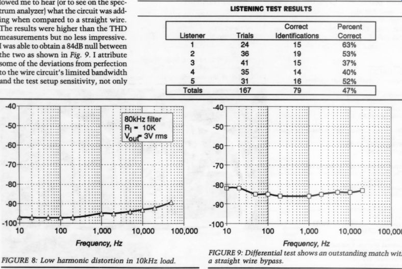
TABLE 2 LISTENING TEST RESULTS
FIGURE 8: Low harmonic distortion in 10kHz load.
FIGURE 9: Differential test shows an outstanding match with a straight wire bypass.
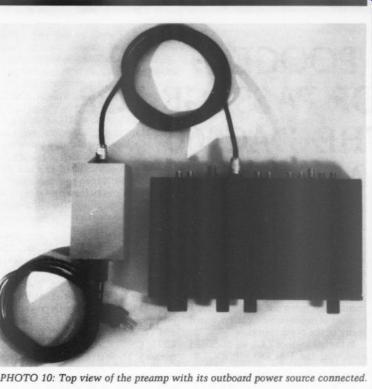
---------- Photo 10.
In fact, when listening with head phones, I needed a booster amp to generate enough volume to even hear the difference signal. If I switched back to the musical source at this setting, it would be un-listenably loud.
As a final test, I used the ABX listening test method. The “A” device was the straight wire with no gain; “B ” was the amplifying circuit set for unity gain.
This test, conducted over a three-month period, is ongoing still. So far, five listeners have used the test setup with the preamp in their systems with each listener living with the equipment for about two weeks. The results varied widely--from seconds to days.
Of the 167 trials conducted thus far, there have been 79 correct identifications as shown in Table 2. This is the predictable “chance' “ outcome you'd expect when there isn't any difference between A' and “B. ” This testing method is so intriguing and requires such excellent experimental design and execution, that it probably merits an essay all its own.
Although the results indicate just the opposite, each of the five participants thought they heard audible differences while testing. Even though several times listeners ascribed the sonic behavior as shifting from A to B or back, they still thought they could hear a difference, though usually slight.
REFERENCES
1. Galo, Gary A., 'Preamp Power Supply, ” TAA 4/90, p. 47.
2. Adelsbach, John, “The Push/Pull Shunt Regulator Revisited, ”“ TAA 4/88, p. 46.
3. Hafler, David, “Build Hafler's XL-10 A/B/D Distortion Test Box, ” TAA 4/87, p. 27.
--------------
Performance Summary
Based on my experiences, I conclude that this preamp circuit is audibly perfect with no discernable distortions added except for the amplified source signal. If you don't like the “sound ” of this preamp, then you don't like the sound from the source. If, on the other hand, you prefer your electronics to alter the music, here is also the circuit with which to start-the perfectly clean canvas onto which you can paint your own blend of euphonic colors.
Tailoring a preamp's “sound” to suit your taste is a lot easier if you begin with a low-distortion wide-bandwidth base. From there, you can add nonlinear elements, alter output impedances, shape frequency responses, modify the “ transfer functions, and "season to taste. ”
All In All
I encourage others to duplicate these methods, measure their own results, and expand on the scientific under standing of audio electronics. Remember, although audio circuit design is a relatively simple branch of the engineering sciences, the pleasure payback is high.
--------------
Also see: