In this installment, the author tackles the power design, explaining the transfer-filter-rectifier arrangement and the accompanying voltage circuits.
The power supply (Fig. 24) is the least complex part of the A40M's design. Even so, it is not as straightforward as it might seem, for there are nuances you must consider.
The grounding scheme is perhaps the most significant area of concern, a fact to which I alluded in the amplifier-design part of this article.
There are, in my mind, three distinct elements to the power supply: the trans former-rectifier, voltage-doubler, and voltage-regulator circuits. Of course, the A40M requires a bipolar power supply.
so there are two of each except for the power transformer. As the builder, you have wide latitude on the specifics of the power supply. However, I recommend the technique I used in this design for the all-important grounding scheme, since it has proved very successful. In what follows, I will describe the design criteria for each of the three power-sup ply elements.
Transformer Primary Circuitry
The purpose of the transformer is twofold: it electrically isolates the power supply and hence the amplifier from the AC power line, and it converts the nominal 117V RMS line voltage to a value better suited to the conversion of the AC to the desired DC voltage level. The former function is nonessential but highly desirable as a safety feature for protection from electrical shock. The latter is also nonessential since other methods exist for converting the voltage up and down. However, these other methods can seldom compete with the efficiency and ease of conversion offered by a power transformer.
Because you can make transformers operate into reactive loads, their primaries and secondaries are rated in volt amperes. (Ratings in watts are reserved for real power delivery.) In all cases, the AC volt-ampere rating of a secondary winding must at least equal-and usually must exceed (sometimes greatly)-the DC power in watts that that winding is designed to deliver to a load. The relationship depends upon the rectification (i.e., half-wave, full- wave center-tapped
[fwct], or full-wave bridge [fwb]), as well as the filter type (i.e., capacitor- or inductor-input).
Although not shown in Fig. 24, I used a power-line filter in the A40M. These filters are cheap, effective against low- and ...
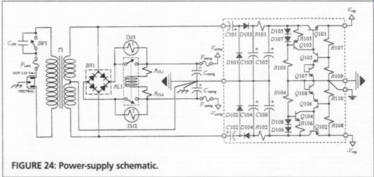
FIGURE 24: Power-supply schematic.
...high-frequency noise on the AC line, and available as an integrated unit of filter and male 3-wire chassis-mount power line connector. Such a filter would simply substitute for the connector shown on the schematic. You should use a unit with a minimum rating of 3A.
I took the connector symbol shown on the schematic from the 1997 ARRL Handbook for Radio Amateurs. Please be very careful to wire the connector ac cording to convention. All three terminal connections are important, and it is critical that you not connect the terminal labeled "HOT" to the chassis.
In general, the power switch should be one designed to switch the power line, and its contacts should have a current rating greater than the current flowing in the primary circuit. In fact, the higher the current rating, the better.
The capacitor Cg that shunts the power switch exists to suppress arcing across the switch terminals during power on or power off. In 1965, I briefly was involved in a NASA project to examine effective means of arc suppression across relay and switch contacts. Simple shunt capacitors were found to be reasonably effective for this purpose and hence are widely used. The capacitor should prolong the life of the switch; it is possible for switch contacts to weld when switching in an inductive circuit.
The fuse F;; . should provide adequate protection to the house wiring. To size such a fuse, determine the total power consumed by the component and divide C102 '+ by the nominal power-line voltage (117V). The quotient is the AC current draw from the power line. Choose a fuse whose current rating is slightly higher than this and whose voltage rating is at least 120V. The A40M consumes roughly 225W, so you should try a 2A fuse. If there is no circuit fault, and a 2A fuse melts, then step up to a 2.25A fuse. I used a slow-blow fuse because in-rush current at power-on would melt a normal 2-A fuse.
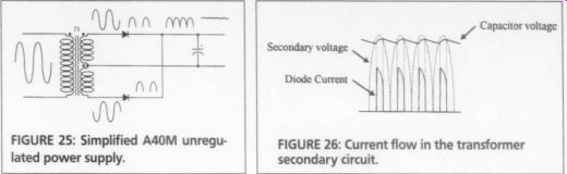
FIGURE 25: Simplified A40M unregulated power supply.
A40M Unregulated Power Supply
This article is not really intended to be a first course in electrical engineering. I assume that the reader has some back ground in the discipline, and therefore I won't discuss the theory of inductance and transformers. Suffice it to say that the turns ratio between primary and secondary windings determines the relative voltage magnitude between them.
In the case of the A40M, the power transformer converts 117V RMS input at the primary winding to a 22V RMS output from each of four independent secondary windings. This 22V RMS is then input to a full-wave rectifier that converts it to a positive (negative for the
[So supply) 120Hz pulse train of amplitude 22v2 - V, = 30V, where V, = 1V is the inevitable voltage drop across a for ward-biased silicon rectifier diode.
The pulse train is pulsating DC and is unusable by the amplifier because it varies from 0 V to 30V and back to 0V 120 times per second. The pulsating DC is peak-detected to a waveform whose average value is about 30V with a small AC ripple voltage superimposed or "riding" on the average DC level. A half-wave rectifier uses a single rectifier diode and consequently provides an output pulse train containing only every other pulse- a 60Hz pulse train.
To be as effective as the full- wave circuit, the capacitor or inductor in a half wave circuit must be twice as large as that of the full- wave circuit. This requires physically larger and more expensive filter capacitors, or inductors, or both, de pending on the filter type. The filter type used in the A40M is called a capacitor input filter for obvious reasons. In high-fidelity applications, half-wave rectification is almost never, if ever, seen. The exception is the A40M, as I will discuss later.
Figure 25 is a simplified version of the A40M unregulated power supply, depicting only the supply producing
The –V_unreg supply operates identically, except that the polarities are every where reversed.
Figure 25 is intended to show the operation of the various components. Thus, the waveforms shown illustrate the step down nature of the transformer, the rectifying action of the diodes, and the smoothing action of the capacitor. There is an artificiality to some of the wave forms. Specifically, there can be only one waveform at any node, including that where the two diodes and the positive terminal of the filter capacitor are connected.

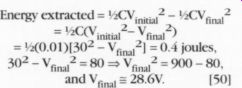
FIGURE 26: Current flow in the transformer secondary circuit. Secondary voltage; Diode Current
The only waveform that would be seen on an oscilloscope attached to this node would be the one at the far right, namely, a DC voltage whose average value would be slightly less than the peak voltage of the positive pulses shown. There would be a slight ripple voltage superimposed upon the DC just as depict ed. This is a reasonable facsimile of the A4OM V output. The –V_reg output would be the mirror image of the V_ output reflected about the 0V axis.
Phasing in Transformer Secondaries
The dots at the tops of the transformer windings indicate their phasing. Thus, the tops of each of the two secondary windings will be at their positive maximum of 31.1V when the top of the primary winding is at its positive maximum of 165.5V, where the lower end of the winding is considered to be the reference, i.e., 0 V.
It is important to recognize this phasing, because, for example, the toroidal transformer used in the A40M had four separate, independent 22V RMS secondary windings from which I formed two independent center-tapped secondaries. I accomplished this by tying the dotted end of one of the four windings to the un-dotted end of a second winding to form a single center-tapped secondary. I connected the remaining two windings in similar fashion to form a second center-tapped secondary.
If you connect two secondaries together so that both dotted ends or both un dotted ends are joined to form the center tap, then the situation is that of two paralleled half-wave rectifiers, and half-wave rectification will be the result. Although paralleling outputs through diodes is generally a safe thing to do, you cannot safely parallel transformer secondaries directly unless they produce exactly the same voltage and are paralleled in-phase, i.e., dot-to-dot.
In the in-phase situation, a current will flow that is equal to the voltage difference between the two windings divided by the sum of their respective resistances. Given the resistances typical of the secondary windings of a power transformer like that in the A40M, tens or even hundreds of amperes can potentially flow. In the out-of-phase parallel connection, a short-circuit across both windings is created, obviously a situation to be avoided.
Many power transformers with multiple secondaries of equal voltage and current ratings are designed to allow paralleled connections, if desired. Al though the voltage is that of a single winding, the current capability doubles.
You can place windings in series, dot-to un-dot, if you wish to attain higher voltage; the current rating will be the lowest rating of any of the series-connected secondaries.
You should not panic. If you use a commercial center-tapped secondary transformer, the phasing is automatically accounted for. Transformers with independent secondaries, such as the ILP used here, come with color-coded secondary windings and a pictorial diagram indicating the proper interconnection for achieving any desired parallel or series configuration.
Ripple and the Filter Capacitor
As shown in Fig. 26, current flow in the transformer secondary circuit can occur only during the time that the voltage at the top of the secondary winding exceeds that at the positive terminal of the filter capacitor by the drop in diode voltage.
The amount of energy stored in a capacitor is 2Cv2, and since C is constant, the energy will fluctuate along with the ripple voltage. Once the diode cuts off, there is no source of energy for the load save that stored in the capacitor. During the cutoff period, the capacitor voltage will fall by an amount that you can deter mine from energy considerations.
Nominally, V,,.... = 30V in the A40M.
Assuming a capacitance of 10,000uF, then a potential energy of 12(0.01)(30)? = 4.5 watt-seconds (joules) is stored in the capacitor. Taking one channel, the power delivered to the amplifier by the | - supply is 1.6A x 30V = 48W. The diode conduction angle is small in a well-filtered supply, a statement the validity of which I hope you will understand in the end. Assuming this to be the case, the capacitor is discharging for almost all the duration of the pulse, and it follows that the capacitor delivers nearly all the energy extracted from the supply during that pulse.
The energy extracted from the capacitor during one pulse is 48 joules/sec + 120 sec! = 0.4 joules, which is less than a tenth of the total energy stored therein If 30V is the fully charged capacitor voltage-that is, the voltage immediately after the diode cuts off and charging current ceases-then (30 - x)V will be the final voltage after the 0.4 joules have been extracted. It is easy to find the final voltage and, hence, the pk-pk ripple voltage x:
The ripple voltage is nearly 1'2V, and then only with a relatively large filter capacitor. The major point, aside from acquiring a quantitative feel for the amount of ripple in the A40M power supply, is gaining an understanding of the relation ship between ripple and the size of the filter capacitor. You can manipulate the relationships shown to derive a usable formula for computing the value of the filter capacitor needed to ensure any desired pk-pk ripple voltage, namely:
C= DC power 60(2Vipigial ~X*) (51]
A good rule of thumb is to limit pk-pk ripple to no more than about 1V. For the A40M, this means a power-supply filter capacitor value of:
DC power 48 "60 @Vipigia -1) 60(2x30-1)
= 13500uF . [52]

Another important inference you can draw is that the larger the capacitor, the shorter the charging period, which is an other way of saying that the conduction angle is smaller. This follows from the observation that, ignoring its voltage drop, the diode conducts only while the instantaneous (AC) voltage at the transformer secondary is greater than the capacitor voltage. However, the capacitor discharges more slowly as its capacitance increases, so its voltage is higher at each point in the discharge period. This necessarily reduces the period during which secondary voltage exceeds capacitor voltage.
The Rectifier
A casual glance suggests that the A40M uses fwb rectification because a bridge rectifier with a 25A rating appears on the schematic. In fact, the | J and -V supplies each use only two of the four diodes in the bridge, and are there fore examples of fwct rectification. Be cause the ILP power transformer has four independent windings, it would have been possible to use true fwb rectification with a separate bridge rectifier for V .. and ~Vinreg: YOU are certainly free to do just that.
The 25A current rating might seem like overly conservative design when only about 3.5A are drawn by the (stereo) amplifier and each diode needs to conduct only half that current on aver age. However, a similar rectifier in one of the 100W monoblocks had a diode failure. Such failures result from very high peak-current flows that are due to the nature of operation of a capacitor input filter and the size of the filter capacitors themselves.
I explored this operation in the previous section. Simply put, a sizable time-in variant energy draw occurs out of the power supply, but the energy must be replenished in short pulses of greater or lesser duration. If the pulse duration is less, the energy-replenishment rate must be correspondingly higher-hence higher peak currents through the diodes.
This is embodied in the concept of the aforementioned conduction angle of the rectifier diodes. The diodes cannot con duct unless and until their anode voltage exceeds their cathode voltage by the for ward voltage drop of the semiconductor junction. In design work, 0.7V is typically used as a rule-of-thumb value for this voltage drop. In power diodes and transistors conducting currents in the ampere range, the figure is closer to a volt, or perhaps even higher.
When one of the rectifier diodes in the fwct rectifier is cut off, its anode (cathode, if it is a negative supply) is physically connected to one end of the secondary.
Its cathode (anode) is effectively connected to the opposite end of the second winding, that is, to the winding on the opposite side of the center tap. The en tire secondary voltage is across the diode.
At a minimum, then, the peak-inverse voltage (PIV) rating of the diode must be 2V_, where V_ = V2 x Vp, is the magnitude (peak) of 1the voltage across either of the center-tapped windings.
In the case of the A40M, this voltage is greater than 60V. To allow for spikes, use diodes whose PIV ratings are several times this value. A 25A bridge with PIV = 400V is not too expensive, and would be a good choice. In an fwb rectifier, only the voltage of a single winding appears across the cutoff diodes; therefore, the PIV requirement is just V_, rather than 2V_. If you elect fwb rectification, then a PIV rating of only 200V is probably adequate.
A disadvantage of the fwb is that the current passes through two diodes; consequently there is an additional one diode forward-voltage loss of about 1V in the DC supply voltage. It is for this very reason that the fwct is often preferred over the fwb rectifier in low-voltage, high-current power supplies.
Limiting Power-on Current Surge
As a quick-and-dirty estimate of the Capacitor (output) voltage E ~~ Diode anode (input) voltage ...
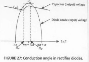
FIGURE 27: Conduction angle in rectifier diodes.
... power-on surge current in the A40M rectifier diodes and trans former secondary, note that Ohm's law demands that i = v/R. In this case, the instantaneous voltage v is the difference between the secondary and the capacitor voltage, and R is the dynamic resistance of the diode plus any wiring resistance, including the secondary winding resistance.
The capacitor voltage is assumed to be zero initially and, because its voltage can change only as a result of current over time, the capacitor looks like a short-circuit. Secondary-circuit resistance R can be as little as 0.1 ohm.
Surge current can be as high as 30/0.1 = 300A if you are so unfortunate as to turn the amplifier on at the moment that the secondary voltage is at its peak.
To protect against such huge power on current surges, the A40M incorporates a surge limiter using KCOOGL negative temperature coefficient (NTC) thermistors. These are sold as inrush-current limiters-the exact purpose for which they are used here. At a nominal ambient temperature of 25°C, the KCOOGL has a resistance of 10 ohm, limiting power-on current to 3A. Under load, it heats up, and its resistance drops to an ohm or less. At this point, however, the capacitor is charged, and there is no power-on surge current with which to contend.
In order to avoid increasing the output resistance of the unregulated power supply by the resistance of the thermistor, a relay short-circuits the thermistor once it has done its job. The operation is simple. As the filter capacitor charges from zero, its voltage finally exceeds 24V, the nominal value at which the relay contacts close, thereby short circuiting the thermistors.
I decided to make the relay circuit draw equally from the V, and -V, supplies, so I used resistors R,, and Rep, to limit the current through the relay coil. This limitation is necessary because Vaves = - Vunreg) = 60V greatly exceeds the 24V rating of the relay coil. In the 100W monoblocks, a 24V zener diode placed across the relay coil guarantees that the rating is not exceeded. This isn't necessary, but R, and R.,, must be properly sized so that the coil voltage does not exceed its rating under normal operation.
The recommended relay and resistor values given work well. There is considerable leeway in relays. The major consideration, in addition to coil current, is that the relay contacts are rated to handle the inrush current. Of course, you can use a single limiting resistor R, =
Rep; * Ry, but its power rating must be double that of either R; , or R¢,.
There is always the possibility that the relay will fail. The KCOO6L thermistor can handle 5A continuous, so there is no safety problem if such a failure occurs.
Bear in mind that if the amplifier is powered off and then repowered before the thermistors have cooled, a surge approaching 100A can occur.
A different scheme employing a triac can avoid this problem by guaranteeing that no current can begin to flow until the secondary AC voltage has made a zero crossing. Thus, the voltage rises at the rate of a sinusoid of 30V magnitude and 120Hz frequency. From the considerations on slew rate and capacitor charging, you can appreciate that this will result in a significantly lower inrush current than would occur if you hit the capacitor with a 30V step-function.
Charging-Current Surge
It is intuitive based on energy considerations that charging-current pulse amplitude must be much higher than the DC current supplied to the load. This some times becomes painfully apparent when rectifier diodes fail-as in the aforementioned 100W monoblock case-despite having a current rating significantly higher than the load current. The designer's problem is to determine the amplitude these pulses are likely to have, and choose a rectifier whose rating comfort ably exceeds it. As an alternative, you might choose to use diodes of lower rating and limit the pulse amplitude below this rating by some means.
During the time a rectifier diode con ducts, it supplies all the current to the load and a charging current to the filter capacitor. In the A40M, load current is about 1.75A for one channel, or 3.5A for two. A 25A bridge has no problem with the load component of the total current.
The charging current is another matter.
The total diode current can be expressed as:
Vioad _ ¢ Av capacitor ip = Road dt
[53]
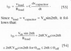
[54]
The approximation is valid in a well-filtered supply, a fact that becomes retrospectively obvious. In this case, 6, is the angle of the sinusoidally shaped voltage pulse (applied to the anode of the diode) at which the diode starts to conduct, and 6, is the angle of that pulse at which the diode ceases conduction. Figure 27 illustrates this nicely.
Because the input-voltage must exceed the capacitor voltage by the diode voltage drop V),, 6, does not occur until after the input voltage and output voltage curves have intersected. During the conduction period, the capacitor charges, and its voltage increases in step with the input voltage as shown, assuming the charging current is not limited. As the input voltage be gins to decline after the V_ apex is passed, a point is reached at which the load current does not discharge the capacitor fast enough to allow output voltage to fall as rapidly as input voltage. The rectifier diode cuts off when this occurs-indicated as 6 _g on the drawing.
The conduction angle is defined as 8,5 - 8,,,- The capacitor voltage lags the charging current and input voltage by 90° (n/2), which is indicated by the co sine rather than the sine function for the expression of the capacitor-charging current. As 2rnft - n/2, cos 2nft - 0. In other words, the maximum value of the charging current occurs at the moment that diode conduction begins, i.e., at

0, ,and: on' Iiy max = 2RfCV, cos6 . [55]
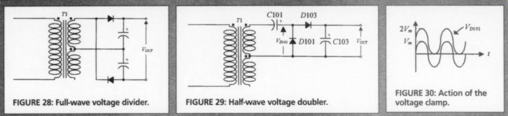
FIGURE 28: Full-wave voltage divider.
FIGURE 29: Half-wave voltage doubler.
FIGURE 30: Action of the voltage clamp.
Reasonable Assumptions
If you can determine the value of 6,__, you on' can also determine the maximum diode charging current and therefore the necessary diode surge-current rating. In fact, with two reasonable simplifying assumptions, you can readily find this angle. Assume that the diode drop is zero, so that the maximum capacitor voltage is V_.
Further assume that this is the point at which the diode cuts off and the capacitor begins to discharge; i.e., assume that diode cutoff occurs at 2nft = 0; = n/2.
Under these assumptions, you can state that:
Pk-pk ripple voltage =AV=V_ -V,
=V,, =V,sin6_.
[56]
Solving for sin yields:
sin, =(V,-AV)/V_, = 6,
=sin [(V,, -AV)/V, |].

[57]
I showed previously the method for determining AV.
For the A40M with a 13,500uF filter capacitor, pk-pk ripple is 1V, and 6, = sin"1([30 - 1]/30) = 75°.
From this, you find that:
ipmax = 2HfCV cos
=2n(120X(0.0135)(30)cos75°
= 79A. [58]

This is a very impressive figure. Also, to it you must add the load current, since that also passes through the diode while it is conducting. Despite the simplifying assumptions, the approximate result is very close to the exact result as long as the RC time constant is large compared to the pulse duration. This is true in the A40M, where RC = 0.25 seconds for C = 13,500uF.
Besides, no precise answer was sought or needed. You should be aware that the surge-current rating of the bridge or other rectifier diodes must be no less than 100A.
As the value of the filter capacitor increases, ip. also increases, because C increases more rapidly than cos de creases in the equation. For example, a 20,000uF capacitor increases charging current to 95A, and even higher diode surge-current ratings would be required.
In the 100W monoblocks, a quick calculation showed charging currents of nearly 300A. No wonder the diode failed! The solution was to replace the 55,000uF filter capacitors with 36,000uF units, and accept the increased ripple.
You should clearly understand that in creasing the value of C shortens the conduction angle both by delaying 6 and causing 6 g to occur earlier. Charging currents increase, with concomitant strains on rectifier diodes and trans former alike. In the limit, 6 = 0 =m/2, and the conduction angle would be zero, a clear impossibility since that would imply infinite charging current. Increasing the value of C also reduces AV, a desirable consequence. As is so often true in electronics in particular and life in general, power-supply design involves a trade-off or two.
Voltage Doubler
In the material about amplifiers, I explained the need for a voltage higher than the main rail voltage. You could devise a power supply producing +35V from a separate center-tapped winding on the main transformer. However, an off-the-shelf transformer with two center-tapped windings at the appropriate current and voltage ratings probably does not exist.
As an alternative, you could use a separate small transformer if you could find one. However, transformers are expensive and bulky, and can produce hum.
Since the current demand on the +35V supplies is not too large, you can form them from the existing transformer by means of a voltage doubler. That is the approach I used here.
Just as full-wave is preferred over half wave rectification, it should be apparent that a full-wave voltage doubler is better than a half-wave one. Consider the full wave voltage doubler in Fig. 28.
Although the capacitors charge only during alternate half-cycles, a la half wave rectifiers, both halves of the input 60Hz sine wave are used, and the ripple frequency is 120Hz. Notice that V is not referenced to the input common (center tap). The output of the full-wav voltage doubler is therefore floating. You cannot use such a circuit in the A40M because the output of the doubler must be referenced to the system ground.
The output of the half-wave voltage doubler in Fig. 29 has a 60Hz ripple frequency. However, the input and output share the system's common reference ground. This circuit is the one used in the A40M to produce a positive voltage.
A similar circuit with component polarities reversed is attached to the lower half of the power-transformer secondary to produce the required negative voltage.
Voltage Clamps Capacitor
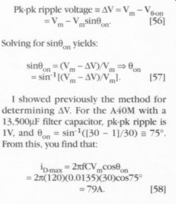
C101 and diode D101 in Fig. 29 form a voltage clamp. A voltage clamp, or simply clamp, fixes one end of a circuit at a given DC reference level. To understand how the circuit works, assume that C101 is discharged, that the AC voltage across the upper winding is zero at time t = 0, and that the voltage at the center-tap will become positive with respect to the upper end of the winding after time zero. As soon as the secondary voltage increases above the forward-voltage drop of D101, current can flow up wards through D101 and begin to charge C101. The capacitor will charge to V_, the peak secondary voltage, which is about 30V in the A40M.
Note that the polarity of C101 must be as shown because of the direction of the charging current. Also note that C101 must consequently have a voltage rating somewhat higher than 30V. As soon as the secondary voltage begins to fall below V_ , the diode will cut off, because its cathode is held at V by C101. After one-half cycle, the voltage at the top of the secondary winding begins to be positive with respect to the center tap. Since D101 is still cut off, no current can flow, and 30V remains across C101. As the negative terminal of C101 rises from zero to +V its positive terminal rises from 30 to 60 V.
The waveform across D101 is the same 30V-amplitude sine wave generated by the upper secondary winding. However, it has been shifted upward by the 30V appearing across C101. Just as its name implies, the clamp has fixed the node to which the center tap, the anode of D101, and the negative terminal of C103 are attached at ground potential (0-V). The waveforms are shown in Fig. 30.
Peak Detector
Diode D103 and capacitor C103 constitute a peak detector, recognizable as a plain old half-wave rectifier. Its input is Vpio01» the 60V pk-pk sine wave shifted upward to produce the pulsating DC voltage shown in Fig. 30. Thus, the output voltage of the doubler is about 60V DC. There will be 60Hz ripple on this voltage because C103 must supply the load current during the time that D103 is cut off. Obviously, the voltage rating for C103 must be greater than 60V.
The main concern in a voltage doubler is that the ripple voltage can become rather high if too much current is drawn from it. This situation is worse because of half-wave rectification, but is otherwise analogous to that in the discussion of the main power supply. For this reason, I simply state that the components and values given for the doubler circuit are satisfactory. You have enough back ground at this point to prove this assertion if you wish.
RC Filter
R101 and C105 (R102 and C106 on the negative side) form a low-pass filter that further reduces AC ripple from the output of the doubler. This is not its only function, however. Due to the inevitable voltage drop across R101 (R102), power dissipation in the pass transistors Q101 and Q102 is reduced, as you shall see. As I have said, the cutoff frequency of this filter is 1/(2 pi RC) = 1Hz with the component values used. This filter will there fore provide 20 log(60/1) = 35dB attenuation of the 60Hz ripple component.
One channel of the A40M drew 85mA from the doubler, while the other channel drew 80mA. Under load, there is a DC voltage level of slightly more than 50V at the doubler output. The 150 -ohm value of R101 results in a 12.75V drop, so that at the RC-filter output, the DC level is about 37V. Power dissipation in R101 and R102 is I ^2 R = 1W, which is why I used 5W wirewound power resistors.
Although the prototype A40M is of dual-mono construction with separate doubler/regulators, it is acceptable to use a single doubler/regulator for both channels. If you do this, however, you must reduce the value of R101 and R102. This will reduce the effectiveness of the RC filter and will increase currents and power dissipation in many of the doubler/regulator components. You must take this into account.
Voltage Regulator
The simplest voltage regulator would consist of one that is zener diode-based. With the ready availability of SW zener diodes, such a regulator would be easy to implement. To the extent that such regulators attenuate AC-ripple, they work on the voltage-divider principle I have already discussed. Consider the simple zener based voltage regulator shown in Fig. 31.
The voltage V,, ... is the desired regulated DC power-supply voltage. Since the zener diode is in parallel or shunt with the load, the regulator is referred to as a shunt regulator. You can satisfactorily model the zener diode as the series combination of a resistor, an ideal diode, and an ideal DC voltage source.
The voltage across the zener diode would be the ideal DC source voltage plus the voltage drop across the resistor due to the current flowing through the zener diode. For simplicity, you need use only the resistor to model the AC behavior in this application.
Essentially, to any AC-ripple component in Vo. the zener diode looks like a resistor, r,, called the dynamic resistance of the diode. Its value is the reciprocal of the slope of the current-voltage (iv) curve of the zener diode at the DC bias point. In other words, if the current through the diode is plotted as a function of the voltage across the diode, a curve results. At each point on this curve, the slope di/dv is the AC or dynamic conductance, and the reciprocal of this value is the dynamic resistance.
As you can see in the zener-diode i-v plot (Fig. 32), i changes rapidly with small changes in v below the knee (breakdown region) in the zener characteristic curve. This corresponds to a large conductance, and consequently to a small resistance. Ideally, this curve would be vertical, connoting zero resistance, so that voltage would be absolutely constant despite current variations.
The steepness of the curve in the break down region is therefore a measure of the "goodness" of the zener-diode as a voltage regulator.
Proper Zener-Diode Operation
The curve in Fig. 32 illustrates some significant points for proper zener-diode operation. If anode voltage is positive with respect to the cathode, the zener diode behaves like an ordinary rectifier diode. In fact, this behavior applies when cathode voltage exceeds anode voltage as long as the magnitude of this differential voltage is less than V,. Voltage V, is the nominal zener voltage. i.e. the voltage that should be seen when the zener is operated at some specified nominal current, I... For simplicity, the diode whose characteristics appear in Fig. 32 is assumed to be the diode in the shunt-regulator schematic (Fig. 31), fortuitously operating at its nominal voltage and current in this well-designed circuit.
Note that the zener diode current is unlimited if the anode-to-cathode voltage across the diode is much greater than +0.7V or less than -V,,. Obviously, the external circuitry must "limit diode current or it will self-destruct. The series resistor R, in the zener-diode shunt-regulator schematic performs this current-limiting function. The resistor value must be high enough to limit current to a value that keeps zener-diode power dissipation V,, x I, within its rating. On the other hand the resistance must be low enough so that the voltage drop across the resistor (due to load current I, , plus zener diode current I) is not excessive.
Excessive means V_in - ---- (I_load + I_z) R_s V_out for this inequality is not true, the zener diode will be operating in that portion of the curve above the breakdown region, where only the reverse saturation current flows. This current is typically in the pico-ampere range, in which you could remove the zener diode from the circuit with negligible effect on circuit behavior, that is, with no regulation occurring. The load voltage in this case would be set by the load current flowing through R_s.
Ever-Changing Slope
The slope of the characteristic curve changes at every point. Even so, if it is assumed that the AC-ripple component is small by comparison with the DC component of Vos then you can use the reciprocal of the slope of the curve at the point defined by V,, .. as the approximate value of r,;. This is not an un reasonable assumption if the regulator is properly designed, since the ripple will, by definition, be small in that case. If you ignore the very small DC voltage drop across the diode dynamic resistance, thea Vo reg = V,, and the zener-diode DC model is an ideal voltage source of magnitude V,, the nominal zener voltage. The DC and AC circuit models appear at the left and right, respectively, of Fig. 33.
You can omit the ideal diode from these models because the zener is operating in the breakdown region, where the diode would be forward-biased. A forward biased ideal diode is simply a short-circuit.
In the DC circuit model, load voltage is zener voltage, and is therefore con stant. You accomplish ideal DC design by setting the value of R; so that zener-diode current is the nominal current that produces V,, the desired output voltage of the regulated supply. Vy-- the aver age DC output voltage from the unregulated power supply, and I,,, ,, is the DC current drawn by the load at V,,, , =V,,.
The formula that determines R_ is then:

[59]
FIG. 33
In the AC model, a simple voltage divider exists. Ignoring load resistance, any AC-ripple voltage vj, entering the regulator from the unregulated power supply divides across R, and r;. Because of this, the AC-ripple at the regulator output, vy rp.
ripple 15 reduced, as you see in the formula:

[60]
Using a typical value, ry = 60€ for a 500mW, 35V zener diode, along with an R, = R101 = 150€, the ripple reduction factor would be [60/(150 + 60)]^-1 = 3.5, or 11dB.
The dynamic resistance of zener diodes with higher power ratings is usually lower. A 5W diode would there fore reduce ripple even more, and you can use a zener-regulator after the RC filter as an alternative to the regulator used in the prototype.
Series Regulator
To reduce and regulate the voltage at the output of the doubler to 36V, a series voltage regulator is used. Q101 in the positive supply and Q102 in the negative are the series-pass transistors, so-called because they are in series with the load rather than in shunt, as was the case for the zener diode-based regulator.
In general, shunt regulators are used in low-power applications or at least in those where the load current is well known and reasonably constant. Based on the previous discussion of the operation of the shunt regulator, the reason for this is obvious. If the load current should drop significantly for any reason, the shunt element must absorb that amount of the load current. This additional current could, in many cases, exceed the power rating of the shunt element.
A series regulator does not suffer from this drawback. In fact, the situation from the standpoint of power dissipation improves in a series regulator as load current falls. However, a shunt regulator is preferable if a short-circuit across the load is a possibility; a series regulator requires protective circuitry in such an event.
This is a feedback regulator. You sample a portion of the output voltage and compare it with a fixed reference voltage. Any difference between the two is an error signal that tends to restore the output voltage to its desired value.
Referring to the schematic (Fig. 24), R107 and R109 (R108 and R110) form a voltage divider that applies the output voltage sample to the base of Q105.
Zener-connected transistor Q107 applies a 7V reference to the emitter of Q105. If the output voltage rises, the consequent rise in the Q105 base voltage (with emitter voltage fixed) causes a rise in base emitter voltage, and that transistor then conducts more heavily. This shunts the base drive away from pass transistor Q101, thereby moving it in the direction of cutoff. This ameliorates the increase in output voltage. The feedback action will similarly counter a decrease in output voltage.
In order to improve performance of the series regulator, a constant-current source consisting of D105, D107, R103, R105, and Q103 (D106, D108, R104, R106, and Q104) provides current for the Q101 (Q102) base and the Q105 (Q106) collector node. This effectively prevents variations in doubler output voltage from adversely affecting the regulation of the feedback circuit.
In order to determine appropriate de sign values for the regulator, consider that load current will be less than 100mA.
Current gain of the pass transistors is typically around 150 at this current level, but it can be lower. Even if this current gain is only 25, the pass transistors need only about 4mA of base drive.
The constant-current source output is determined by ( Vis + Vipy07 + Vaggi03) R103. All three voltages represent for ward-biased diode voltage drops, so that all should be roughly equal to 0.7V. Since Q103 is a pnp device, Vgi 03 is a negative 0.7V. Thus, I.
source = 0-7/100 = 7mA.
In the worst case, then, 4mA of this current will provide Q101 base drive with the remaining 3mA shunted through Q105 and Q107. This is a nice little circuit that provides proper bias levels for all involved components and good performance.
The output voltage is determined by:
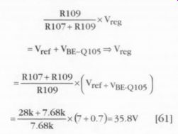
[61]
Power Dissipation in the Pass Transistor
The power dissipation in the series-pass element is frequently a major design consideration in series regulators. Ignoring the small dissipation in the base emitter circuit, it is easy to calculate this dissipation since:
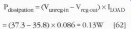
[62]
I used a heatsink for Q101 and Q102, but clearly it was not necessary, since those 30W devices are perfectly capable of dissipating a watt or so to ambient air.
Note that collector-emitter voltage V is only 1.5V across these transistors, which comes very close to their saturation voltage. No regulation can occur when the series-pass elements are in saturation, so this is a condition to be avoided. The criteria is that even under conditions of minimum Vin-unreg' Vee 5 Vin-unreg
= Vout_reg 2 1V, since V will be slightly less than 1V.
Since I am unwilling to change the A40M prototype, this is notification to you that it might be better to increase Vi. to several volts. This you can readily accomplish simply by reducing the value of R101 and R102 from 150-ohm to 100 or 120 ohm. This will lower the effectiveness of the R101-C105 (R102-C106) filter and increase the dissipation in Q101 (Q102).
While these effects are undesirable, they will have little impact upon regulator function. Once again, a trade-off must be made between conflicting requirements.
Saturation
Voltage Doubler/Regulator Grounding
You probably noticed in Fig. 24 that the ground trace for the doubler/regulator board is discontinuous. As in the amplifier circuit, this is part of the star ground philosophy that attempts to minimize adverse circuit effects due to grounding problems.
In the case of the doubler/regulator, voltage and current "spikes" will occur in the doubler portion because of the capacitor-charging pulses in C101 and C103 (C102 and C104). By breaking the ground trace, the spikes in the ground return go directly to the star-ground point without passing through the regulator ground trace, which is independently and directly returned to the star ground point.
The principle is that the impedance at the star-ground point is so low that it attenuates ground spikes to an insignificant level. To ensure this, the A40M prototype uses a heavy brass bus block to connect the common terminals on the main power-supply filter capacitors. The center point of this block is the star ground point.
With this background, it's now time to turn our attention to the amp layout and construction, which I'll cover in the next installment.
by: By Norman E. Thagard
Also see: