This technique that replaces diodes with power MOSFETs in your power supplies can significantly improve efficiency.
In some low-voltage high current power supplies, losses are incurred by using pn-junction silicon power diodes for the rectification process. The diodes' approximate 0.6V of forward volt age drop presents, in some instances, a factor that severely limits the efficiency of converting AC to DC. In a bridge circuit, the result is 1.2V of total drop, which can be an unacceptably significant loss in a 5 or 6V supply.
Recently, the trend is to use Schottky diodes instead, which have a drop of about 0.4V. This seemingly small difference between the pn-junction type and the Schottky can sometimes be the difference between a supply that works and one that doesn't.
The Synchronous-Rectification Alternative
In the ideal power supply, the rectifying diode would have zero resistance and an efficiency of 100%, with no voltage drop.
Under those conditions, a load would be able to draw as much power as a power transformer could deliver. Unfortunately, diodes are not perfect. Is there, then, no alternative to diodes? In certain circumstances, one other technique turns out to have even better efficiency than diodes, but it is a little more exotic. The idea is called synchronous rectification (SR), but don't let the name scare you; it's not that complicated.
Instead of diodes, an SR circuit uses power MOS-FET transistors acting as switches. The term synchronous rectification derives from the fact that the signal to the gate of the MOSFETs is synchronized--via a special transformer--with the AC voltage to be rectified. SR is a system that is more efficient at the AC/DC conversion process than diodes, especially in the area below 50V, depending on the application.
Power MOSFETs are the key to the circuit primarily because, among many other positive attributes, they have a very low on-state resistance during saturation.
Some MOSFETs have less than 0.1 ohm in their conduction state, with no pn-junction voltage drop. This means that it is possible to achieve a voltage drop of less than 0.6V, and even less than 0.4V.
The typical SR circuit in Fig. 1 is a full wave grounded center-tap configuration with two special features: two n-channel power MOSFETs and a special power transformer with extra windings at each end of the secondary. These auxiliary end windings supply the synchronizing control signal to the gates of the transistors.
When the AC voltage to the source of Q1 goes positive, for instance, the volt age at its gate goes even more positive with respect to the source, and Q1 turns on, allowing power to flow to the drain.
When the AC voltage flips direction, Q1 turns off, and Q2 turns on in the same manner. In this way, the transistors act as one-way switches, and a full-wave rectified voltage appears at the drains.
Transistor Positioning
You may notice that transistors Q1 and Q2 seem to be installed backwards. In other MOSFET circuits, the drain lead is usually made more positive than the source lead, but here it is the other way around. One of the beauties of MOSFET transistors is that you can make voltage and current flow either way through the device: either drain-to-source or source to-drain. In this circuit, I use source-to drain. This is necessary because of the presence of the MOSFET's intrinsic diode. I'll come back to this internal diode later.
To make this system work, you must operate the MOS-FETs as switches. This means the transistors are switched from cutoff to saturation and back again. To do this, the gate voltage must be of the proper amplitude and bias, and--sinc you are dealing with AC--the proper phase. Even though they can be operated in either direction, the transistors need a positive voltage at the gate with respect to the source in order to turn them on (but no real current). This voltage must be greater than 10V peak, but less than 20V peak to avoid possible device destruction.
A gate voltage between 10 and 20V will cause channel saturation. This is true of all power MOSFETs. Zero or negative voltage at the gate with respect to the source will ensure channel cutoff. This is where the special transformer-secondary auxiliary windings come into play. Notice the phasing dots on the transformer.
Since you are dealing with AC, the correct phase will also ensure the correct biasing of the transistors.
Special Transformer
One look at this special transformer will tell you that it must be a custom-made job that would cost big bucks if you could find someone to make it for you. Is there another way? Yes. Power transformer T1
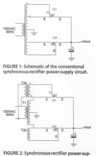
FIGURE 2: Synchronous-rectifier power-supply circuit, where T1 is the power
transformer and T2 is a small dual 12V transformer to bias the MOSFET gates.
(Fig. 2) is the one to use. It may be of any voltage and current capability, as long as you find power MOSFETs that can work with those ratings.
Remember that this system works best for voltages of less than 50V peak. This operating area is where the very low on state resistance n-channel MOS-FETs can be found. With your voltage and current requirements known, select the type with the lowest on-state resistance avail able-the lower the better.
T2 is the special transformer that supplies the gate-bias voltages. For T2, I obtained through Digi-Key a normal 10V, low-current transformer that has the feature of dual, separate secondaries. I could have used two separate transformers, but the fact that it has two secondaries makes it perfect for my synchronous application. One thing to note about transformers is that the output voltage is rated according to the load current. Since the MOSFET's high-gate impedance does not present a load and consequently no current is drawn, the output voltage will be higher than advertised.
These 10V windings produce about 19V peak AC, which is fine for the gate voltage. But all transformers are different; there is no real way to tell whether a specific one can be used in this circuit, except by measuring the peak voltage.
Anything smaller than 10V peak is not going to be able to put the transistors into saturation, and anything larger than 20V peak could destroy them (check the MOSFET manufacturer's specs for gate voltage limit).
120V AC 60Hz
Adjusting the Voltages
Carefully observing the phase relation ship, connect T2 to T1 as in Fig. 2 Make sure that the voltages from each side as measured from the center-tap are equal and that they increase in value as you move from the sources to the gates.
You can fix any discrepancy by reversing the connections to the offending winding on T2.
When you are sure that the voltages are correct, connect Q1 and Q2 to the circuit. With no filter capacitor connected as yet, observe the pulsating DC voltage on an oscilloscope. The waveform should show a full-wave rectified signal that looks like the waveform a regular diode circuit would produce. Next, connect the oscilloscope across one of the transistors, drain-to-source. There should be no fractional voltage drop, as there would be with a diode circuit.
-----------
FURTHER READING:
"Application Notes 5.6, 6.6
Irving M. Gottlieb, fourth
------------
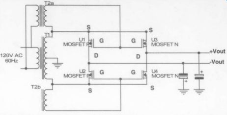
FIGURE 3
You may wonder about using an SR for negative voltages. No problem. Replace the n-channel MOSFETs of Fig. 2 with p channel power MOSFETs. The two transformer connections will remain the same, as well as the gate, source, and drain connections. The drains will output a negative voltage with respect to the center tap. The only drawback with this circuit is that the MOSFET manufacturers have so far been unable to make the on state resistances for the p-channel version as low as the n-channel versions. Still, use the lowest available.
Going one step further, Fig. 3 shows a grounded center-tap bridge circuit that produces dual complementary outputs.
The n-channel transistors produce the positive voltage, while the p-channels produce the negative. Because it uses the auxiliary transformer T2, the main transformer T1 can be any voltage and current type you desire. Also, T1 can be a grounded center-tap or no center-tap, depending on your application.
The Intrinsic Diode
All MOSFETs have an intrinsic diode integrated between the source and drain. This diode must not come into play in these circuits. If it does, the result is not a synchronous rectifier, but a regular diode rectifier, and you must avoid this at all costs.
As far as the diode is concerned, there are a few things to watch for that indicate this undesirability and a malfunction.
A 0.6V drop across any transistor means that the MOSFET's intrinsic diode, in stead of the transistor itself, is performing the rectification. This could be caused by problems such as loss of the gate signal, an insufficient amount of gate-signal amplitude to turn the transistor on, opening up of the channel material in the transistor, or excessive current draw causing the normal voltage drop across the transistor to exceed the diodes' 0.6V forward bias. Any of these conditions indicate that SR is not occurring.
Since a MOSFET transistor has a positive temperature coefficient for on-state resistance, the more current that is drawn through the device, the larger on-state resistance will be, due to heating, and thus the larger the voltage drop across it. So to keep the intrinsic diode inactive, good heatsinking is definitely required. Remember also, that MOSFET devices are sensitive to static electricity, so always wear a grounded wrist strap when handling them, and always handle them by the body, not the leads.
When it comes to power supplies that need to produce a large amount of current at a low voltage, and where diodes just won't cut it, try synchronous rectification. Its complexity as compared to the usual measures is not that daunting. With these suggestions and information I have provided, and in the right circumstances, you can make this efficient rectifier system perform much better than diodes.
--------
Also see: