This article explores how a square wave can tell you volume about an audio device's performance.
A square wave is a periodic waveform that alternates for equal periods of time between two fixed levels, with a transition time between the levels that is negligible when compared with the dwell times at each. Since the waveform is symmetrical, the duty cycle is 0.5.
A square wave is useful in audio testing [1-2] because its spectrum is composed of a series of odd-harmonic sine waves whose amplitudes decrease in proportion to the harmonic order. The square wave is a function of:
sin(x) + sin(3x)/3 + sin(5x)/5 + sin(7x)/7+… + sin((2n - Dx)/2n -1).
A function generator is commonly used as a square-wave signal source, although you could also use a square TTL logic pulse-train generator if it were capacitive-coupled to the unit under test (UUT).
It is also important to recognize the limitations of square-wave testing. As Norman Crowhurst said, "While square waves of appropriate frequency can serve as a quick check of the approximate nature of both magnitude and phase response in the vicinity of low- and high-frequency turnovers, too much trust should not be placed in a good resultant square-wave response. It gives absolutely no indication of nonlinear distortion.
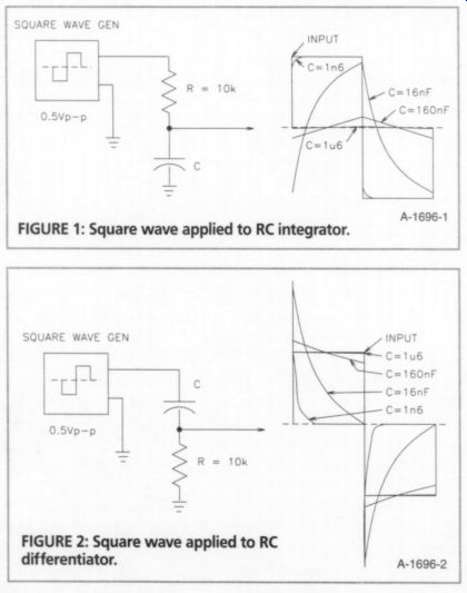
FIGURE 1: Square wave applied to RC integrator. FIGURE 2: Square wave applied
to RC differentiator.
Passive RC Circuits
First let's review what happens when a 1kHz square wave is impressed on a passive RC circuit arranged as an integrator, as shown in Fig. 1.
When the -3dB f_c frequency of the RC network is 100khz (R=10 khz, C = 1n6), you can see a slight rolloff on the leading edge of the square wave as the higher harmonics are attenuated in proportion to their frequency. This is noticeable even though the -3dB frequency is 100 times the fundamental square-wave frequency of 1kHz.
When I increase C to 16nF (f-c = 10kHz, or ten times the fundamental frequency), the rolloff is more severe. It doesn't even reach the 250mV peak level of the square wave at the end of each half-cycle.
If you increase C to 160nF (f. =1kHz), the square wave is integrated into a triangle wave shape whose peak amplitude reaches only 38mV. Circuit analysis reveals that the integral of a step function is a linear ramp if the step rise time is very small compared with the time it takes for the network to achieve a steady-state response. Finally, with C equal to 1u6 (f_c = 100Hz), the triangle wave peaks at only 2.5mV.
When a 500mV pk-pk 1kHz square wave is impressed on a passive RC circuit arranged as a differentiator, as shown in Fig. 2, you see a different result. When the RC network frequency is 100Hz (R = 10k, C = 1u6), you can see a slight downward slope from the leading edge to the trailing edge of the square wave response. This slight reduction in low-frequency response is called tilt.
When C is decreased to 160nF (f_c = 1kHz, the fundamental frequency), the tilt is more severe. The leading edge increases to a 290mV peak, and the trailing edge drops to 213mV. If you decrease C to 16nF (f. = 10kHz), the leading edge increases to 480mV peak, and the trailing edge falls to zero.
Finally, with C equal to 1n6 (f_c = 100kHz), the waveform is a series of alternating positive and negative spikes whose peak voltage is 500mV.
Circuit analysis shows that the derivative of a step function is an impulse if the step rise time is very large compared with the time it takes for the net work to achieve a steady-state response.
RC integrators are often used at the inputs to amplifying circuits to filter out radio-frequency interference, and at the output of a CD player's DAC current-to-voltage converter cir to further roll off oversampling artifacts. Examples of RC differentiator circuits are the input coupling capacitor for any amplifier, and the coupling caps used to drive the output tubes in a tube amplifier. The waveforms in Figs. 1 and 2 illustrate the care that is required in designing and applying these circuits.
Test Simulations
Rather than set up a physical amplifier circuit, I thought it would be interesting to create a generic noninverting op-amp circuit in SPICE, and vary the values of | two capacitors to roll off the high- or low-frequency response. I used a third capacitor to induce high-frequency peaking.
The simulation circuit is shown in Fig. 3. Cf and Rf are the feedback components, Cg and Rg are the gain-setting components, and C_in is the composite common-mode and differential-mode input capacitance of the op amp, along with any parasitic capacitance that occurs in real-world circuitry. The SPICE simulation makes it very easy to vary component values. After each simulation run, I can plot the AC-analysis frequency or phase response, and the transient analysis response such as you would see on an oscilloscope.
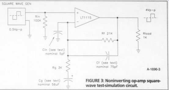
FIGURE 3: Noninverting op-amp square-wave test-simulation circuit.
In order to introduce a lower phase margin, I used the LT1115 op-amp macro model,3 since it is only stable for voltage gains 210. I purposely set the simulation model to a voltage gain of 8, or about 18dB. (The frequency-response plots will show flat response as +12dB, because I needed to offset the simulation program's 0-500mV square-wave genera tor by -250mV to obtain an input signal that is symmetrical about zero. This results in an output shift, after amplification, of -2V DC, or -6dB, relative to the signal generator's normal ground reference. I checked to see that I made this correction throughout the article but, un fortunately, I am also the proofreader.) The baseline design uses the capacitor values marked "nominal" in Fig. 3, which produce a +3dB bandwidth of 1Hz to 100kHz. Cg reduces the DC gain to unity, and rolls off the low-frequency response.
The -3dB frequency is determined by
fl= . 1/2nRgCg Cf
introduces a feedback pole that rolls off the high-frequency response. The -3dB frequency is determined by:
gy 1 2mRfCf
Cf also counteracts the zero introduced by C_in that causes gain peaking at high frequencies. If Cf were removed, C_in and the combined parallel resistance of Rf and Rg would determine the peaking frequency. Since C_in shunts the series gain-setting network Rg and Cg, it causes the overall gain to grow with increasing frequency.
In addition, the common-mode components of C_in represent the input-stage junction capacitances, and these vary with the square root of the applied junction voltages. An AC signal at the op-amp input causes these capacitances to change with the signal, producing small variations in the closed-loop gain. These gain variations cause high-frequency distortion, but they are always present in a noninverting op amp, and cannot be cancelled by Cf.
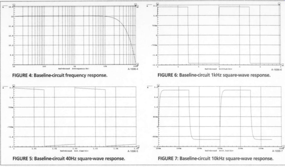
FIGURE 4: Baseline-circuit frequency response.
FIGURE 5: Baseline<circuit 40Hz square-wave response.
FIGURE 6: Baseline-circuit 1kHz square-wave response.
FIGURE 7: Baseline-circuit 10kHz square-wave response.
Simulations
In order to simulate real-world test conditions, I used square waves with frequencies of 40Hz, 1kHz, and 10kHz. These are the generally accepted test frequencies for evaluating the response of amplifiers, preamps, and sources.
The frequency-response plot of the baseline Fig. 3 circuit simulation is shown in Fig. 4 (dB versus freq). The square-wave response to a 40Hz square wave, shown in Fig. 5, produces mini mal tilt. The square-wave response to a 1kHz square wave (Fig. 6) is nearly ideal.
The square-wave response to a 10kHz square wave (Fig. 7) shows a slight rolloff on the leading edges, with no peaking or oscillation.
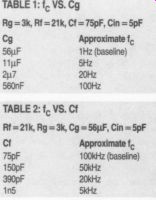
TABLE 1: , VS.Cg Rg = 3k, Rf =21k, Cf = 75pF, Cin =5pF Cg Approximate 56uF
1Hz (baseline) 11uF 5Hz 2u7 20Hz 560nF 100Hz TABLE 2: f. VS. Cf Rf =21k, Rg
= 3k, Cg =56F, Cin =5pF Ct Approximate f, 75pF 100kHz (baseline) 150pF 50kHz
390pF 20kHz nS 5kHz
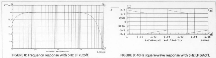
FIGURE 8: Frequency response with 5Hz LF cutoff. FIGURE 9: 40Hz square-wave
response with 5Hz LF cutoff.
There is another interesting observation here. I delayed the display of the two cycles of square-wave response to allow Cg to charge, but in the 10kHz plot, the output has not yet settled to a level that is symmetrical about 0V. The positive peaks are +3V, and the negative peaks are--1V.
The SPICE-simulation settling time at 10kHz would have been very long, so I compromised. The result is a visible DC component, which decreases with time and eventually reaches zero.
In each case, the square-wave output is representative of a well-behaved amplifier circuit with excellent audio-frequency response. Now I'll proceed to mess it all up.
Low-Frequency Limiting
I modified the circuit of Fig. 3 to deliberately limit the low-frequency (LF) response by reducing the value of Cg. I used the values in Table 1, which also gives the resultant f. cutoff frequency for each value of Cg.
The first run was with the circuit modified for a 5 Hz LF cutoff. The frequency response plot is shown in Fig. 8. The response to a 40Hz square wave is shown in Fig. 9. You can see that the tilt is more pronounced than it was with the 1Hz LF cutoff in Fig. 5.
When I repeated the simulation with a 1kHz wave, Fig. 10 shows no evidence of LF tilt. The reason is simple. A 1kHz square wave contains no frequency components below its fundamental frequency, and the -3dB Cg-Rg 5Hz LF cutoff frequency does not cause any attenuation at 1kHz.When performing square-wave testing, you must use a test frequency suitable for the cutoff frequency range you're investigating.
Next I changed Cg to 2u7, to further limit the LF response to 20Hz. The frequency-response plot is shown in Fig. 11, and the response to a 40Hz square wave is shown in Fig. 12. You can see that the tilt is now much more pronounced. And remember, the response is still within what some consider to be acceptable LF audio response; that is,-3dB down at 20Hz. Now you see why amplifier designers extend the LF-response cut off as low as they do.
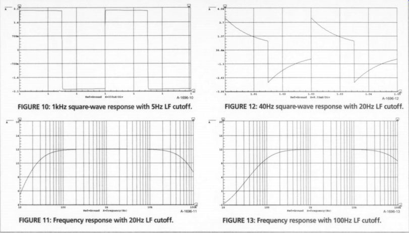
FIGURE 10: 1kHz square-wave response with 5Hz LF cutoff
FIGURE 11: Frequency response with 20Hz LF cutoff.
FIGURE 12: 40Hz square-wave response with 20Hz LF cutoff.
FIGURE 13: Frequency response with 100Hz LF cutoff.
[...]
d ever, it is not really noticeable in the full screen display.
The final LF simulation uses an above band cutoff of 100Hz, where Cg is changed to 560nF. The frequency-response plot is shown in Fig. 13, and the response to a 40Hz square wave is shown in Fig. 14. It is interesting that when I used a 1kHz square wave, there was visible evidence of LF tilt, as you can see in Fig. 15. Yet the attenuation is only -0.05dB, and the phase shift is only +4°.
High-Frequency Limiting
Next, I modified the circuit of Fig. 3 to deliberately limit the high-frequency (HF) response by increasing the value of Cf. I used the values in Table 2, and re turned Cg to its baseline value of 56uF.
First I increased Cf to 150pF, which reduces the HF response -3dB at 50kHz.
The frequency response for this circuit is shown in Fig. 16, where I shifted the frequency scale out to 1IMHz. The response below 1kHz is unchanged from that shown in Fig. 4.
The simulation run in Fig. 77 using a 10kHz wave shows a bit more leading edge rolloff than the baseline plot in Fig. 7. Repeating the simulation with both 40Hz and 1kHz square waves produced results identical to those shown in Figs. 5 and 6. Again, this illustrates the importance of selecting the proper square wave frequency for the frequency range you wish to examine. Even though a 40Hz square wave contains ultrasonic harmonics, they are at levels that are only 0.4% (-48dB) of those contained in the 10kHz square wave, and the effect of the reduced HF response is not noticeable on an oscilloscope.
Next I increased Cf to 390pF, for a HF cutoff of 20kHz. The frequency-response plot is shown in Fig. 18. The response to a 10kHz square wave is shown in Fig. 19.
The leading-edge rolloff is now much more pronounced, yet the response is still within what some consider to be acceptable HF response; that is, -3dB down at 20kHz. You can see why amplifier designers extend the HF response cutoff as high as they do.
The final LF simulation uses a below band cutoff of 5kHz, where Cf is 1n5.
The frequency-response plot is shown in Fig. 20, and the response to a 10kHz square wave is shown in Fig. 21. 1 also ran simulations with 40Hz and 1kHz square waves. As you can see in Fig. 22, the drastic reduction in the HF response now makes it quite noticeable in the 1kHz square wave. The 40Hz response is still identical to Fig. 5.
Simultaneous Low-Frequency and High-Frequency Limiting
For this simulation I limited the -3dB bandwidth to 40Hz-10kHz, using values of Cg = 12 and Cf = 750pF. The frequency response is shown in Fig. 23. The responses to 40Hz and 10kHz square waves are essentially identical to those of
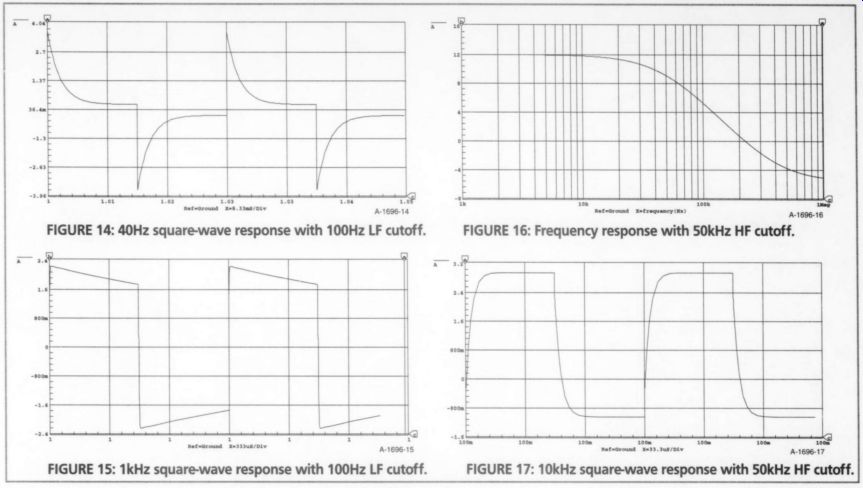
FIGURE 14: 40Hz square-wave response with 100Hz LF cutoff. ; FIGURE 15: 1kHz
square-wave response with 100Hz LF cutoff. FIGURE 16: Frequency response with
50kHz HF cutoff. FIGURE 17: 10kHz square-wave response with 50kHz HF cutoff.
[...]
High-Frequency Peaking
I introduced high-frequency peaking by decreasing the value of Cf to 1pF, with all other capacitors at their baseline values. The feedback now allows a theoretical -3dB response to 8MHz. However the LT1115 has a minimum gain-bandwidth product of 40MHz (fo = 20kHz).
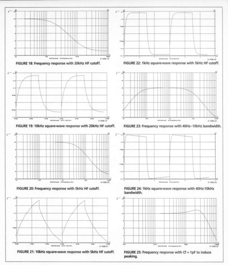
FIGURE 19: 10kHz square-wave response with 20kHz HF cutoff.
FIGURE 21: 10kHz square-wave response with 5kHz HF cutoff.
FIGURE 23: Frequency response with 40Hz-10kHz bandwidth.
...would require a minimum gain-band width of 64MHz to achieve a voltage gain of 8, so this circuit will run into the possibly unstable limit imposed by the op amp gain-versus-frequency curve. This shows the importance of proper compensation in any feedback circuit.
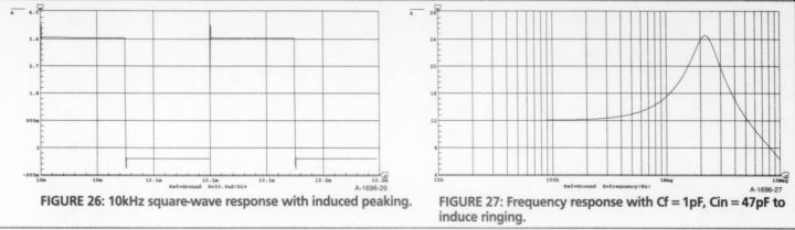
The frequency-response plot in Fig. 25 shows a 19.4dB peak at about 2.3MHz, with a -35° phase angle. (You must add the 13.4dB shown in Fig. 25 to the 6dB amplified signal-generator off set, explained earlier in the Test Simulations section.) I shifted the frequency scale to a range of 10kHz-10MHz. The response to a 10kHz square wave is shown in Fig. 26. Each leading edge has a single peak of about 0.45V above the square wave. This peak was also noticeable with a 1kHz square wave, but not with the 40Hz square wave (neither shown).
In an under-compensated circuit, it is possible to cause HF peaking during input-stage troubleshooting with just the added capacitance of test probes or inputs.
FIGURE
26: 10kHz square-wave response with induced peaking. FIGURE 27: Frequency
response with Cf = 1pF, Cin =47pF to i= A induce ringing.
High-Frequency Ringing
To induce high-frequency damped oscillation or ringing, I left Cf at 1pF, while increasing Cin to 47pF, an admittedly un realistic value. The frequency-response plot in Fig. 27 shows a sharp +31dB peak at about 2.2MHz, with a -30° phase angle. The response to a 10kHz square wave is shown in Fig. 28. Each leading edge has five damped cycles with the first cycle reaching a peak of 1.7V above the square wave.
High-Frequency Oscillation
Oscillation occurred when I increased C_in to 120pF, an even more unrealistic value. The frequency response plot in Fig. 29 shows a sharp +43dB peak at about 1.6MHz, with a -25° phase angle.
The response to a 10kHz squarewave is shown in Fig. 30. The oscillations reach a peak of about 3V above the square wave and, although damped, are continuous.
I repeated the test with a 1kHz square wave. Here the oscillations died out be fore the start of the next vertical transition, as you can see in Fig. 31. You can easily induce steady-state oscillation by increasing C_in to 220pF.
The output stage of the LT1115 can swing +13.5V with +/- 15V DC supplies. At 1kHz (A = 18dB) it takes a 1.2V RMS input signal to drive the output to its maximum. The simulation shows that at 1.6MHz (A = 43dB), it takes only a 96mV RMS input signal to achieve maximum output.
However, if you look at the typical gain-versus-frequency curves for the LT1115, you see that it has only about 20dB of voltage gain at 1.6MHz, with a 45° phase margin. Still, a stray RF signal could possibly overload the amplifier, assuming no HF attenuation network at the front end.
I removed all the capacitors from the SPICE model and made Rf and Rg equal to the LT1115's specified large-signal voltage gain of 1.5 x 10° (1.5V/uV with a 1k load, or about 124dB) to see where the simulation frequency response would roll off. It showed a slightly optimistic 30dB gain at 1.6MHz, with 75° - phase margin, but yielded only 56dB ...
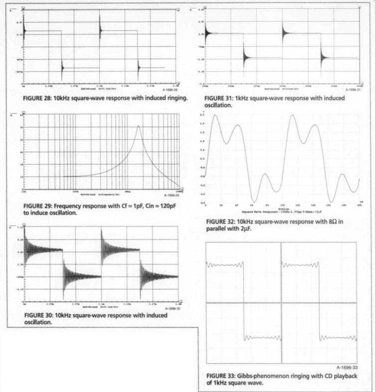
FIGURE 28: 10kHz square-wave response with induced ringing.
FIGURE 29: Frequency response with Cf = 1pF, Cin = 120pF
FIGURE 31: 1kHz square-wave response with induced oscillation.
FIGURE 32: 10kHz square-wave response with 8-ohm in parallel with 2pF.
FIGURE 33: Gibbs-phenomenon ringing with CD playback of 1kHz square wave.
... gain at 1kHz, whereas the published curve shows about 95dB. The simulation gain curve crossed 0dB at about 33MHz, versus 25MHz for the published curve.
SPICE simulations always need a reality check against the published specifications. The macro models are a compromise, and sometimes become inaccurate at the extremes of performance. My in tent is to show the square-wave responses for various bandwidths, and I believe that the SPICE simulations work well for these comparative purposes, even if the absolute results have some error.
There is one more situation that can induce ringing in a 10kHz square wave.
One of the tests for power-amplifier stability is a load of 8-ohm in parallel with 2uF.
Most amplifiers will show almost no effect from this reactive load, which is designed to simulate an electrostatic speaker. For some amplifiers, however, this load can induce peaking at ultrasonic frequencies and produce the oscillations shown in Fig. 32.
Digitally Sampled Square Wave
The square wave in Fig. 33 is that of a CD player, playing the 1002.27 Hz square wave test track 16 on the CBS Records CD-1 Test Disc (available from Old Colony Sound Lab as CD1). The ringing shown in the figure is not the result of in stability, but portrays the Gibbs phenomenon. This ripple is introduced in the analog output of the CD player because of the finite bandwidth determined by the 44.1kHz sampling frequency. The lack of odd sine frequencies above 22kHz in the sampled square wave causes ringing at the edges of the waveform.
References
. Norman Crowhurst, Audio Measurements, Audio Amateur Press (available from Old Colony SoundLab s BKAA41).
. Bob Metzler, Audio Measurements Handbook, Audio Precision, Inc. (available from Old Colony Sound Lab as BKAP2).
. Linear Technologies LT1115 Data Sheet, 1992Linear Databook Supplement, pp. 2-82 through 2-93; also linear-tech.com.
. Arfken, G., "Mathematical Methods for Physicists," in Gibbs Phenomenon, 3rd Ed., pp. 783-787,Academic press, 1985.
--------
Also see:
Upgrading Monarchy's Converters and Amplifiers