Active systems such as audio amplifiers operate by drawing current from some voltage source--ideally with a fixed and unvarying output-and transforming this into a variable voltage output that can be made to perform some useful function, such as driving a loudspeaker, or some further active or passive circuit arrangement. For most active systems, the ideal supply voltage would be one having similar characteristics to a large lead-acid battery: a constant voltage, zero voltage ripple, and a virtually unlimited ability to supply current on demand. In reality, considerations of weight, bulk, and cost would rule out any such Utopian solution and the power supply arrangements will be chosen, with cost in mind, to match the requirements of the system they are intended to feed.
However, because the characteristics of the power supply used with an audio amplifier have a considerable influence on the performance of the amplifier, this aspect of the system is one that cannot be ignored.
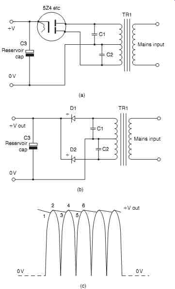
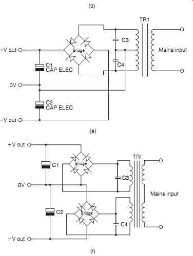
FIG. 1 : Full-wave rectifier systems.
1 High Power Systems
In the early days of valve-operated audio systems, virtually all of the mains-powered DC power supply arrangements were of the form shown in FIG. 1(a) , and the only real choice open to the designers was whether they used a directly heated rectifier, such as a 5U4, or an indirectly heated one, such as a 5V4 or a 5Z4. The indirectly heated valve offered the practical advantage that the cathode of the rectifier would heat up at roughly the same rate as that of the other valves in the amplifier so there would not be an immediate switch-on no-load voltage surge of 1.4, the normal HT supply output voltage.
With a directly heated rectifier, this voltage surge would always appear in the interval between the rectifier reaching its operating temperature, which might take only a few seconds, and the 30 s or so that the rest of the valves in the system would need to come into operation and start drawing current. Using an indirectly heated rectifier would avoid this voltage surge and would allow lower working voltage components to be used with safety in the rest of the amplifier. This would save cost. However, the directly heated rectifier would have a more efficient cathode system and would have a longer working life expectancy.
Although there are several other reasons for this, such as the greater ease of manufacture, by the use of modern techniques, of large value electrolytic capacitors, or the contemporary requirement that there shall be no audible mains hum in the amplifier output signal due to supply line AC ripple, it is apparent that the capacitance values used in the smoothing, decoupling, and reservoir capacitors in traditional valve amplifier circuits are much smaller than in contemporary systems, which operate at a lower output voltage. The main reason for this is that the stored energy in a capacitor is defined by the relationship:
ECV c _ 1 2 2
… where E c is the stored energy, in joules; C is the capacitance, in farads; and V is the applied voltage. This means that there is as much energy stored in an 8- µ F capacitor, charged to 450 V, as there is in a 400- µ F capacitor charged only to 64 V. Because the effectiveness of a decoupling capacitor in avoiding the transmission of supply line rubbish, or a power supply reservoir capacitor in limiting the amount of ripple present on the output of a simple transformer/rectifier type of power supply, depends on the stored charge in the capacitor, its effectiveness is very dependent on the applied voltage, as is the discomfort of the electrical shock that the user would experience if he or she inadvertently discharged such a charged capacitor through his or her body.
2 Solid-State Rectifiers
The advent of solid state rectifiers-nowadays almost exclusively based on silicon bipolar junction technology-effectively caused the demise of valve rectifier systems, although for a short period, prior to the general adoption of semiconductor rectifiers, gas-filled rectifiers, such as the 0Z4, had been used, principally in car radios, in the interests of greater circuit convenience because, in these valves, the cathode was heated by reverse ionic bombardment so that no separate rectifier heater supply was required. The difficulties caused by the use of these gas-filled rectifiers were that they had a relatively short working life and that they generated a lot of radio frequency (RF) noise. This RF noise arose because of the very abrupt transition of the gas in the cathode/anode gap of the rectifier from a nonconducting to a conducting state. The very short duration high current spikes this caused shock excited the secondary windings of the transformer-and all its associated wiring interconnections-into bursts of RF oscillation, which caused a persistent 100- to 120-Hz rasping buzz called modulation hum to appear in the audio output.
The solution to this particular problem was the connection of a pair of capacitors, shown as C1 and C2 in FIG. 1(a) , across the transformer secondary windings to retune any shock-excited RF oscillation into a lower and less invasive frequency band. Sometimes these modulation hum prevention capacitors are placed across the rectifiers or across the mains transformer primary winding, but they are less effective in these positions.
With modern, low conduction resistance, semiconductor diodes, low equivalent series resistance (ESR) reservoir capacitors, and low winding resistance (e.g., toroidal) transformers, this problem can still arise, and the inclusion of these capacitors is a worthwhile and inexpensive precaution. The circuit layout shown in FIG. 1(b) is the PSU arrangement used in most contemporary valve amplifiers. For lower voltages, a wider range of circuit layouts are commonly used, also shown in FIG. 1 .
3 Music Power
In their first flush of enthusiasm for solid-state audio amplifiers, manufacturers and advertising copy writers collectively made the happy discovery that most inexpensive audio amplifiers powered by simple supply circuits, such as that shown in FIG. 1(b) , would give a higher power output for short bursts of output signal, such as might quite reasonably be expected to arise in the reproduction of music, than they could give on a continuous sine-wave output. This short-duration, higher output power capability was therefore termed the music power rating, and, if based on a test in which perhaps only one channel was driven for a period of 100 ms every second, would allow a music power rating to be claimed that was double that of the power given on a continuous tone test in which both channels are driven simultaneously (the so-called rms output power rating).
4 Influence of Signal Type on Power Supply Design
Although this particular method of specification enhancement is no longer widely used, its echoes linger on in relation to modern expectations for the performance of hi-fi equipment. The reason for this is that in the earlier years of recorded music reproduction there were no such things as pop groups, and most of those interested in improving the quality of recording and replay systems were people such as Peter Walker of Quad or Gerald Briggs of Wharfedale Loudspeakers, whose spare-time musical activities were as an orchestral flautist and a concert pianist and whose interests, understandably, were almost exclusively concerned with the reproduction, as accurately as possible, of classical music. Consequently, when improvements in reproduction were attempted, they were in ways that helped enhance the perceived fidelity in the reproduction of classical music and the accuracy in the rendition of the tone of orchestral instruments. In general, this was easier to achieve if the electronic circuitry was fed from one or more accurately stabilized power supply sources, although this would nearly always mean that such power supplies would have, for reasons of circuit protection, a fixed maximum current output. While this would mean that the peak power and the rms power ratings would be the same, it also meant that there would be no reserve of power for sudden high-level signal demands-a penalty that the tonal purists were prepared to accept as a simple fact of life.
However, times change and hi-fi equipment has become easier to accommodate, less expensive in relative terms, and much more widely available. Also, there has been a considerable growth in the purchasing power of those within the relatively youthful age bracket, most of whose musical interests lie in the various forms of pop music--preferably performed at high signal levels-and it is for this large and relatively affluent group that most of the hi-fi magazines seek to cater.
The ways in which these popular musical preferences influence the design of audio amplifiers and their power supplies relate, in large measure, to the peak short-term output current that is available since one of the major instruments in any pop ensemble will be a string bass, whose sonic impact and attack will depend on the ability of the amplifier and power supply to drive large amounts of current into the LS load, and it must do this without causing any significant increase in the ripple on the DC supply lines or any loss of amplifier performance due to this cause.
A further important feature for the average listener to a typical pop ensemble is the performance of the lead vocalist, commonly a woman, the clarity of whose lyric must not be impaired by the high background signal level generated by the rest of the group.
Indeed, with much pop music, with electronically enhanced instruments, the sound of the vocalist, although also enhanced electronically, is the nearest the listener will get to a recognizable reference sound. This clarity of the vocal line demands both low intermodulation distortion levels and a complete absence of peak-level clipping.
The designer of an amplifier that is intended to appeal to the pop music market must therefore ensure that the equipment can provide very large short-duration bursts of power; that the power supply line ripple level, at high output powers, must not cause problems to the amplifier; and that, when the amplifier is driven into overload, it copes gracefully with this condition. The use of large amounts of NFB, which causes hard clipping on overload, is thought to be undesirable. Similarly, the effects of electronic (i.e., fast acting) output transistor current limiting circuitry (used very widely in earlier transistor audio amplifiers) would be quite unacceptable for most pop music applications so alternative approaches, mainly based on more robust output transistors, must be used instead.
In view of the normal lack in much pop music of any identifiable reference sound source, such as would be provided by the orchestral or acoustic keyboard instruments in classical music forms, a variety of descriptive terms has emerged to indicate the success or otherwise of the amplifier system in providing attractive reproduction of the music. Terms such as "exciting," "giving precise image location," "vivid presence," "having full sound staging," "blurred," or transparent are colorful and widely used in performance reviews, but they do not help the engineer in his attempts to approach more closely to an ideal system performance-attempts that must rely on engineering intuition and trial and error.
5 High Current Power Supply Systems
In order for the power supply system to be able to provide high output currents for short periods of time, the reservoir capacitor, C3 in FIG. 1(b) , must be large and have a low ESR value. Ideally, the rectifier diodes used in the power supplies should have a low conducting resistance, the mains transformer should have low resistance windings and low leakage inductance, and all the associated wiring, including any PCB tracks, should have the lowest practicable path resistance. The output current drawn from the transformer secondary winding, to replace the charge lost from the reservoir capacitor during the previous half cycle of discharge, occurs in brief, high current bursts in the intervals between the points on the input voltage waveform labeled 1 and 2, 3 and 4, 5 and 6, and so on, shown in FIG. 1(c) . This leads to an output ripple pattern of the kind shown in FIG. 1(d) . Unfortunately, all of the measures that the designer can adopt to increase the peak DC output current capability of the power supply unit will reduce the interval of time during which the reservoir capacitor is able to recharge. This will increase the peak rectifier/reservoir capacitor recharge current and will shorten the duration of these high current pulses. This increases the transformer core losses, both the transformer winding and the lamination noise, and also the stray magnetic field radiated from the transformer windings. All of these factors increase the mains hum background, both electrical and acoustic, of the power supply unless steps are taken-in respect of the physical layout, and the placing of interconnections--to minimize it. The main action that can be taken is to provide a very large mains transformer, apparently excessively generously rated in relation to the output power it has to supply, in order that it can cope with the very high peak secondary current demand without mechanical hum or excessive electromagnetic radiation. Needless to say, the mains transformer should be mounted as far away as possible from regions of low signal level circuitry; its orientation should be chosen so that its stray magnetic field will be at right angles to the plane of the amplifier PCB.
6 Half-Wave and Full-Wave Rectification
Because the reservoir capacitor recharge current must replace the current drawn from it during the nonconducting portion of the input cycle, both the peak recharge current and the residual ripple will be twice as large if half-wave rectification is employed, such as that shown in the circuit of FIG. 1(h) , in which the rectifier diode only conducts during every other half cycle of the secondary output voltage rather than on both cycles, as would be the case in FIG. 1(b) . A drawback with the layouts of both Figures 1(a) and 1(b) is that the transformer secondary windings only deliver power to the load every other half cycle, which means that when they do conduct, they must pass twice the current they would have had to supply in, for example, the bridge rectifier circuit shown in FIG. 1(e) . The importance of this is that the winding losses are related to the square of the output current (P = i x R) so that the transformer copper losses would be four times as great in the circuit of FIG. 1(b) as they would be for either of the bridge rectifier circuits of FIG. 1(f) . However, in the layout of FIG. 1(b) , during the conduction cycle in which the reservoir capacitor is recharged, only one conducting diode is in the current path, as compared with two in the bridge rectifier setups.
Many contemporary audio amplifier systems require symmetrical _ ve and _ ve power supply rails. If a mains transformer with a center-tapped secondary winding is available, such a pair of split-rail supplies can be provided by the layout of FIG. 1(e) or, if component cost is of no importance, by the double bridge circuit of FIG. 1(f). The half-wave voltage doubler circuit shown in FIG. 1(g) is used mainly in low current applications where its output voltage characteristic is of value, such as perhaps a higher voltage, low-current source for a three-terminal voltage regulator.
7 Direct Current Supply Line Ripple Rejection
Avoidance of the intrusion of AC ripple or other unwanted signal components from the DC supply rails can be helped in two ways: by the use of voltage regulator circuitry to maintain these rails at a constant voltage or by choosing the design of the amplifier circuitry that is used so that there is a measure of inherent supply line signal rejection.
In a typical audio power amplifier, there will be very little signal intrusion from the _ ve supply line through the constant current source, Q6 and Q7, because this has a very high output impedance in comparison with the emitter impedance of Q1 and Q2, so any AC ripple passing down this path would be very highly attenuated. However, there would be no attenuation of rubbish entering the signal line via R5, so that, in a real-life amplifier, R5 would invariably be replaced by another constant current source, such as that arranged around Q7 and Q8.
For the negative supply rail, the cascode connection of Q10 would give this device an exceedingly high output impedance, so any signal entering via this path would be very heavily attenuated by the inevitable load impedance of the amplifier. Similarly, the output impedance of the cascode-connected transistors Q3 and Q4 would be so high that the voltage developed across the current mirror (Q5 and Q6) would be virtually independent of any _ ve rail ripple voltage. In general, the techniques employed to avoid supply line intrusion are to use circuits with high output impedances wherever a connection must be made to the supply line rails. In order of effectiveness, these would be a cascode connected field-effect transistor or bipolar device, a constant current source, a current mirror, or a decoupled output, such as a bootstrapped load. HT line decoupling, by means of an LF choke or a resistor and a shunt-connected capacitor, such as R2 and C2, was widely used in valve amplifier circuitry, mainly because there were few other options available to the designer. Such an arrangement is still a useful possibility if the current flow is low enough for the value of R2 to be high and if the supply voltage is high enough for the voltage drop across this component to be unimportant. It still suffers from the snag that its effectiveness decreases at low frequencies where the shunt impedance of C2 begins to increase.
FIG. 2 : Simple shunt regulators.
8 Voltage Regulator Systems
Electronic voltage regulator systems can operate in two distinct modes, each with their own advantages and drawbacks: shunt and series. The shunt systems operate by drawing current from the supply at a level that is calculated to be somewhat greater than maximum value, which will be consumed by the load. A typical shunt regulator circuit is shown in FIG. 2(a) , in which the regulator device is an avalanche or Zener diode or a two terminal band-gap element for low current, high stability requirements. Such simple circuits are normally only used for relatively low current applications, although high power avalanche diodes are available. If high power shunt regulators are needed, a better approach is to use a combination of avalanche diode and power transistor, as shown in FIG. 2(b) . The obvious snag is that in order for such a system to work, there must be a continuous current drain that is rather larger than the maximum likely to be drawn by the load, which is wasteful. The main advantages of the shunt regulator system are that it is simple and that it can be used even when the available supply voltage is only a little greater than the required output voltage. Avalanche and Zener diodes are noisy, electrically speaking, although their noise can be lessened by connecting a low ESR capacitor in parallel with them. For applications where only a low voltage is needed and its actual value is not very important but a low circuit noise is essential, a simple arrangement is to use a string of silicon diodes, as shown in FIG. 2(c) . Each of these diodes will have a forward direction voltage drop of about 0.6 V, depending on the current flowing though them. Light-emitting diodes have also been recommended in this application, for which a typical forward voltage drop would be about 2.4 V, depending on the LED type and its forward current. All of these simple shunt regulator circuits will perform better if the input resistor (R1) is replaced by a constant current source, shown as CC1.
9 Series Regulator Layouts
The problem with the shunt regulator arrangement is that the circuit must draw a current that is always greater than would have been drawn by the load on its own. This is an acceptable situation if the total current levels are small, but this would not be tolerable if high output power levels were involved. In this situation it is necessary to use a series regulator arrangement, of which some simple circuit layouts are shown in FIG. 3 . The circuit of FIG. 3(a) forms the basis for almost all of this type of regulator circuit, with various degrees of elaboration. Essentially, it is a fixed voltage source to which an emitter-follower has been connected to provide an output voltage (that of the Zener diode less the forward emitter bias of Q1) at a low output impedance. The main problem is that for the circuit to work, the input voltage must exceed the output voltage-the difference is termed the drop-out voltage-by enough voltage for the current flow through R1 to provide the necessary base current for Q1 and also enough current through D1 for D1 to reach its reference voltage. Practical considerations require that R1 shall not be too small.
In a well-designed regulator of this kind, such as the 78xx series voltage regulator IC, the drop-out voltage will be about 2V.
This drop-out voltage can be reduced by reversing the polarity of Q1, as shown in FIG. 3(b) , so that the required base input current for Q1 is drawn from the 0-V rail. This arrangement works quite well, except that the power supply output impedance is much higher than that of FIG. 3(a) , unless there is considerable gain in the NFB control loop. In this particular instance Q2 will conduct and feed current into the Q1 base until the voltage developed across R3 approaches the voltage on the base of Q2, when both Q2 and Q1 will be turned off. By augmenting Q2 with an op-amp, as shown in FIG. 4, a very high performance can be obtained from this inverted type of regulator layout.
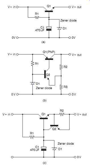
FIG. 3 : Simple series regulators.
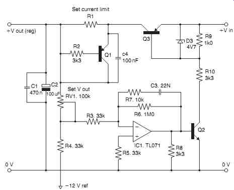
FIG. 4 : Series-stabilized PSU.
10 Overcurrent Protection
A fundamental problem with any kind of solid-state voltage regulator layout, such as that of FIG. 3(a) , is that if the output is short-circuited, the only limit to the current that can flow is the capacity of the input power supply, which could well be high enough to destroy the pass transistor (Q1). For such a circuit to be usable in the real world, where HT rail short-circuits can, and will, occur, some sort of overcurrent protection must be provided. In the case of FIG. 3(c) , this is done by putting a resistor (R2) in series with the regulator output and then arranging a further transistor (Q2) to monitor the voltage across this. If the output current demand is enough to develop a voltage greater than about 0.65 V across R2, Q2 will conduct and will progressively steal the base current from Q1.
In the inverted stabilizer circuit shown in FIG. 4 , R1 monitors the output current, and if this is large enough to cause Q1 to conduct, then the output voltage will progressively collapse, causing the PSU to behave as a constant current source at whatever output voltage causes the load to draw the current determined by R1. (I know this protection technique works because this is the circuit I designed for my workshop bench power supply 20 years ago, 1…
…which has been in use every working day since then, having endured countless inadvertent output short-circuits during normal use, as well as surviving my son having left it on overnight, at maximum current output, connected to a nickel-plating bath that he had hooked up, but which had inadvertently become short circuited.) In the particular layout shown, the characteristics of the pass transistors used (Q3 and its opposite number) are such that no current/voltage combinations that can be applied will cause Q3 to exceed its safe operating area boundaries, but this is an aspect that must be borne in mind. Although I use this supply for the initial testing of nearly all my amplifier designs, it would not have an acceptable performance, for reasons given earlier, as the power supply for the output stage of a modern fi-fi amplifier.
However, there is no such demand for a completely unlimited supply current for voltage amplifier stages or preamplifier supply rails, and in these positions, a high-quality regulator circuit can be of considerable value in avoiding potential problems due to hum and distortion components breaking through from the PSU rails. Indeed, there is a trend in modern amplifier design to divide the power supplies to the amplifier into several separate groupings: one pair for the gain stages, a second pair for the output driver transistors, and a final pair of unregulated supplies to drive the output transistors themselves. Only this last pair of supplies normally needs to be fed directly from a simple high current rectifier/reservoir capacitor type of DC supply system.
A further possibility that arises from the availability of more than one power supply to the power amplifier is that it allows the designer, by the choice of the individual supply voltages provided, to determine whereabouts in the power amplifier the circuit will overload when driven too hard since, in general, it is better if it is not the output stage that clips. This was an option that I took advantage of in my 80-W power MOSFET design of 1984.
11 Integrated Circuit (Three Terminals) Voltage Regulator ICs
For output voltages up to 24V and currents up to 5A, depending on voltage rating, a range of highly developed IC voltage regulator packages are now offered, having overcurrent (s/c) and thermal overload protection, coupled with a very high degree of output voltage stability, and coupled with a typical _ 60-dB input/output line ripple rejection. They are available most readily in _ 5 V and _ 15V/_ 15V output voltages because of the requirements of 5-V logic ICs and of IC op-amps, widely used in preamplifier circuits, for which 15-V supply rails are almost invariably specified.
Indeed, the superlative performance of contemporary IC op-amps designed for use in audio applications is such an attractive feature that most audio power amplifiers are now designed so that the maximum signal voltage required from the pre amp is within the typical 9.5-V rms output voltage available from such IC op-amps.
Higher voltage regulator ICs, such as the LM337T and the LM317T, with output voltages up to _ 37 and _ 37 V, respectively, and output currents up to 1.5 A are available but where audio amplifier designs require higher voltage-stabilized supply rails, the most common approaches are either to extend the voltage and current capabilities of the standard IC regulator by adding on suitable discrete component circuitry, as shown in FIG. 5 , or by assembling a complete discrete component regulator of the kind shown in FIG. 6 .
In the circuit arrangement shown for a single channel in FIG. 5 , a small-power transistor, Q1, is used to reduce the 55- to 60-V output from the unregulated PSU to a level that is within the permitted input voltage range for the 7815 voltage regulator IC (IC2). This is one of a pair providing a 15-V DC supply for a preamplifier. A similar 15-V regulator IC (IC1) has its input voltage reduced to the same level by the emitter- follower Q4 and is used to drive a resistive load (R7) via the control transistor, Q5. If the output voltage, and consequently the voltage at Q5 base, is too low, Q5 will conduct, current will be drawn from the regulator IC (IC1), and, via Q4, from the base of the pass transistor, Q2. This will increase the current through Q2 into the output load and will increase the output voltage. If, however, the output voltage tends to rise to a higher level than that set by RV1, Q5 will tend toward cutoff and the current drawn from Q2 base will be reduced to restore the target output voltage level.
Overcurrent protection is provided by the transistor Q3, which monitors the voltage developed across R4 and restricts the drive to Q2 if the output current is too high.
Safe operating area conformity is ensured by the resistor R3, which monitors the voltage across the pass transistor and cuts off Q2 base current if this voltage becomes too high.
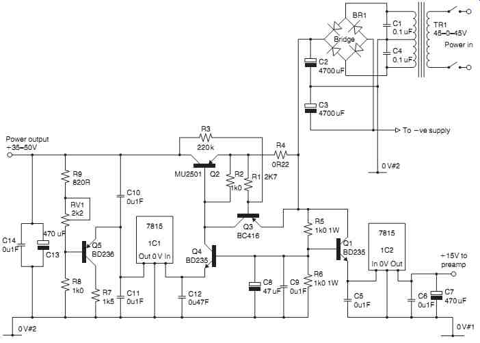
FIG. 5 : Stabilized PSU (one-half only shown).
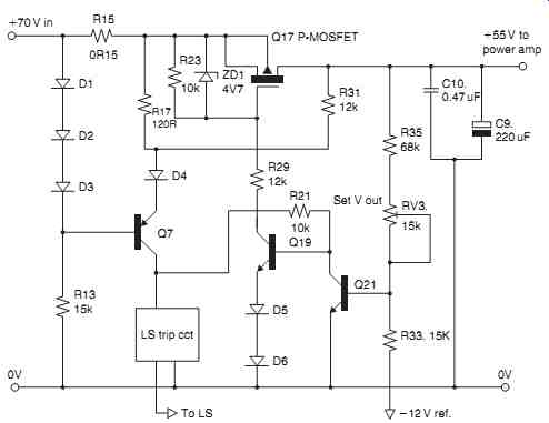
FIG. 6 : S/C-protected PSU.
In the circuit of FIG. 6 , which is used as the power supply for an 80- to 100-W power MOSFET audio amplifier-again only one channel is shown-a P-channel power MOSFET is used as the pass transistor and a circuit design based on discrete components is used to control the output voltage. In this, transistor Q21 is used to monitor the potential developed across R33 through the R35/RV3 resistor chain. If this is below the target value, current is drawn through Q19 and R29 to increase the current flow through the pass transistor (Q17). If either the output current or the voltage across Q17 is too high, Q7 is cut off and there is no current flow through Q18 into Q17 gate.
This regulator circuit allows electronic shut down of the power supply if an abnormal output voltage is detected across the LS terminals (due, perhaps, to a component failure). This monitoring circuit (one for each channel) is shown in FIG. 7 . This uses a pair of small-signal transistors, Q1 and Q2, in a thyristor configuration, which, if Q2 is turned on, will connect Q1 base to the 0-V rail, which, in turn, causes current to be drawn from Q2 base, which causes Q2 to remain in conduction even if the original input voltage is removed. The trip voltage will arise if an excess DC signal (e.g., _ 10 V) appears across the LS output for a sufficient length of time for Q1 to charge to _ 5 V. Returning to FIG. 6 , when the circuit trips, the forward bias voltage present on Q19 base is removed and Q17 is cut off and remains cut off until the trip circuit is reset by shorting Q2 base to the 0-V rail. If the fault persists, the supply will cut out again as soon as the reset button is released. An electronic cut-out system like this avoids the need for relay contacts or fuses in the amplifier output lines. Relays can be satisfactory if they are sealed, inert gas-filled types, but fuse holders are, inevitably, crude, low-cost components, of poor construction quality, and with a variable and uncertain contact resistance. These are best eliminated from any signal line.
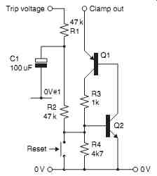
FIG. 7 : Trip circuit.
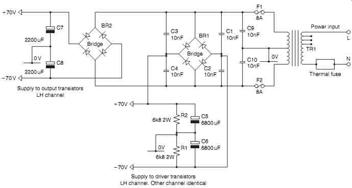
FIG. 8 : Rotel rhb10 PSU (only one channel shown).
12 Typical Contemporary Commercial Practice
The power supply circuit used in the Rotel RHB10 330-W power amplifier is shown in FIG. 8 as an example of typical modern commercial practice. In this design two separate mains power transformers are used, one for each channel (the drawing only shows the LH channel-the RH one is identical) and two separate bridge rectifiers are used to provide separate 70-V DC outputs for the power output transistors and the driver transistors. This eliminates the distortion that might otherwise arise because of breakthrough of signal components from the output transistor supply rail into the low power signal channel. Similarly, use of a separate supply system for each channel eliminates any power supply line-induced L-R cross talk that might impair stereo image positioning.
13 Battery Supplies
An interesting new development is the use of internally mounted rechargeable batteries as the power supply source for sensitive parts of the amplifier circuitry, such as low input signal level gain stages. Provided that the unit is connected to a mains power line, these batteries will be recharged during the time the equipment is switched off, but will be disconnected automatically from the charger source as soon as the amplifier is switched on.
14 Switch-Mode Power Supplies
Switch-mode power supplies are widely used in computer power supply systems and offer a compact, high efficiency regulated voltage power source. They are not used in fi-fi systems because they generate an unacceptable level of HF switching noise due to the circuit operation. They would also fail the requirement to provide high peak output current levels.
== == ==