By Benjamin Hinrichs
The modular design and flexibility of the microcontroller program allow the preamplifier to be built exactly according to the individual requirements of its user.
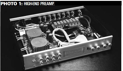
PHOTO 1: HIGH-END PREAMP.
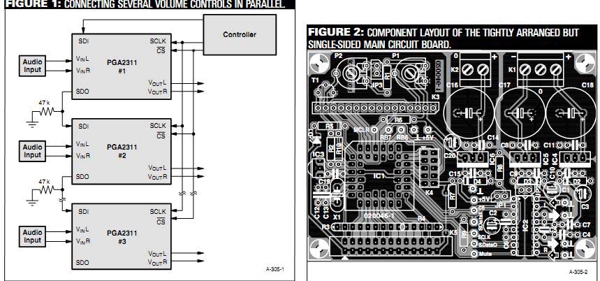
FIGURE 1: CONNECTING SEVERAL VOLUME CONTROLS IN PARALLEL. FIGURE 2: COMPONENT
LAYOUT OF THE TIGHTLY ARRANGED BUT SINGLE-SIDED MAIN CIRCUIT BOARD.
Reproduced, with permission, from May '04 Elektor Electronics magazine, 2004 Segment B.V., Beek (Lb.), The Netherlands, www.segment.nl.
The multitude of options for constructing your "personalized" high-end preamplifier means that you must read this second part of the article before you order the parts and take up your soldering iron. This is because your requirements determine how many circuit boards of which type you will need, as well as which components you will need. You can connect several volume controls in parallel as illustrated in Fig. 1, in order to adjust more than two channels at the same time. If you do this, you must interconnect the CS, Mute, SCLK, +5V, and Ground terminals of the circuit boards.
SADATO from the first circuit board is connected to SDATI of the next circuit board, and so on. This causes the volume level set ting to be communicated to all of the circuit boards.
You can choose from traditional audio signal switching, switching the ground leads together with the signal leads, or switching balanced signals. If you know how, you can also give the microcontroller additional functionality or modify the details in the software, such as the designations shown on the display.
POPULATING THE BOARD
What we need now are a few instructions for populating the main pre amplifier board. This is because the circuit board shown in Fig. 2 is quite compact. The closely spaced, narrow tracks are not particularly forgiving of mistakes, so the components should be fitted properly the first time, and solder splashes and overheated joints should be assiduously avoided.
On the main circuit board, only JP1 and JP3 can be implemented as jumpers.
JP2 (directly underneath IC2) is a wire bridge. There is another wire bridge at the inner edge of K5, which should be fitted immediately: done is done! Now you should consider whether the programming and/or paralleling ...
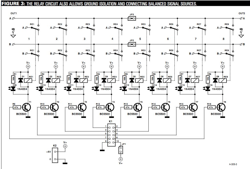
FIGURE 3: THE RELAY CIRCUIT ALSO ALLOWS GROUND ISOLATION AND CONNECTING
BALANCED SIGNAL SOURCES.
... connections are necessary. If you arrive at a positive conclusion after studying the two text boxes, then you must fit the associated connectors (refer to the components list) and the solder pins for the audio signals. Despite all the claims to the contrary, it certainly makes sense to fit the solder pins before the other components. Generally speaking, they need a bit of coaxing, and some times they can only be pressed into the holes using (brute) force. Besides this, a 1.3mm diameter silver-plated steel pin requires a considerable amount of heat to achieve a reliable bond with the solder. And if you find a solder pin standing at an angle to the board, you can start all over again. This can be the kiss of death for small, sensitive components that have already been fitted in the immediate vicinity.
If you use a decent stuffing frame, it doesn't matter very much if the low-pro file components (resistors, capacitors, and diodes) are only fitted afterwards. As always, proper polarization is important for some of the components. Besides the diodes and small electrolytic capacitors, this also includes the resistor arrays and the PLCC socket, which is beveled on one corner. This marking must match the component overlay on the circuit board.
Now is the right time to not fit LED D1 if you want to use it as a pilot light on the front panel. This LED, along with IR receiver IC3, should only be soldered in place after the circuit board has been securely fitted in the enclosure and the two components have been fastened in holes drilled in the front panel. If your en closure layout does not permit the circuit board to be placed directly behind the front panel and you thus must fit the IR receiver off the board, a screened connection cable is mandatory.
The fixed voltage regulators IC4-IC6, which should be soldered in place after pin headers K3-K5 and the high-quality DIL socket for the PGA2311 have been fitted, do not require heatsinks.
The soldering work is completed with the fitting of the three large electrolytic capacitors and the two circuit-board terminal strips (K1 and K2).
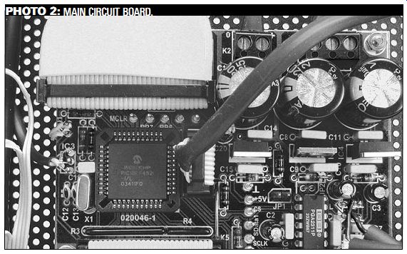
PHOTO 2: MAIN CIRCUIT BOARD.
If you wish to control several volume control boards in parallel, fully populate one main circuit board and fit only the portion with the PGA2311 (including the peripheral circuitry and the voltage regulator circuitry) on the other boards.
The system has been tested using a single controller board and two parallel circuit boards. All of the necessary connection points are located in a row on the circuit board.
CHANNEL SWITCHING
The input channels are switched on the relay board. The circuit shown in Fig. 3 allows two different wiring options.
With the traditional option, all eight inputs from the Cinch sockets are used, with a single output to the main circuit board. This requires JP2 and JP3 to be fitted. Each relay is then responsible for one stereo channel. If standard twin screened audio cable is used, one channel is connected to A and the other to B, and the screen braid is soldered to the bottom of the circuit board.
Ground isolation, which may be de sired to improve channel separation or avoid interconnecting the grounds of different items of equipment connected to the preamplifier, can be achieved by switching not only the signal lines, but also the associated ground potentials.
In this case, for each channel the "live" lead is soldered to A and the ground lead is soldered to B. In addition, jumpers JP2 and JP3 are left open. In this mode, each pair of relays (RE1 & RE5, RE2 & RE6, RE3 & RE7, and RE4 & RE8) belongs to a single signal source.
This yields four stereo inputs and two sets of outputs (OUT1A & OUT1B and OUT2A & OUT2B). Here again A corresponds to the "live" lead and B to ground. The only other thing you have to do is to change the Input Type option in the Set-up menu to "Double." In order to handle balanced signals, we simply switch two relays simultaneously. In this mode, you also have to add a second, parallel volume control and then connect the balanced signals to one of the input channels (such as Left In) on both volume controls. This works well-quite well, in fact.
Fujitsu (formerly Takamisawa) type RY-5W-K relays are used here. Naturally, other pin-compatible types could also be used, but the specified line has excel-lent characteristics and is available for less than 2 euros (approx. £1.40, $2.30), for example from Conrad Electronic (www.conrad.de). This is a plastic-encapsulated relay, which prevents any dust from accumulating inside. The contacts are made from a silver-palladium alloy with supplementary gold plating.
Power for the relay board is taken from the main circuit board via connector K1 (which requires jumper JP1 to be fitted). If you wish to treat the channel switching board to its own power supply or you want to use this board in a different project, you can also connect a 5V supply to the K2 terminals.
In order to avoid overloading the microcontroller outputs, transistors with base resistors are used as relay drivers. Diodes D1-D8 act as freewheeling diodes, while LEDs D9-D16 provide a visual indication of the relay states.
The LEDs do not necessarily have to be fitted to the circuit board (Fig. 4); they can of course be fitted to the front panel instead if you want to do without the display, or they can simply be omitted (along with their series resistors).
JP1 can be implemented as a jumper, but JP2 and JP3 should be implemented as wire bridges. Otherwise there's not anything particularly remarkable about populating the circuit board, particularly if you use the components specified in the components list and everything fits perfectly.
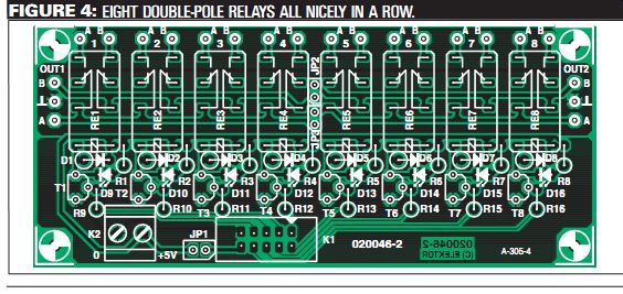
FIGURE 4: EIGHT DOUBLE-POLE RELAYS ALL NICELY IN A ROW.
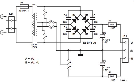
FIGURE 5: THE MAINS POWER SUPPLY CAN PROVIDE UNIPOLAR OR SYMMETRIC OUTPUT
VOLTAGES.
STABLE SUPPLY
A large part of the stabilization, decoupling, and hum suppression for the sup ply voltages takes place locally on the main circuit board, for both the digital portion (+5V) and the analogue portion (5V). The only other thing you need is a sufficiently stable source of symmetrical DC voltages (which shouldn't be a problem with the low current consumption). This provides an opportunity to use a general-purpose low-power mains power supply (Fig. 5).
The power supply is designed to use Talema 10-VA encapsulated low-profile toroidal transformers (see reference 2), which can be obtained from DigiKey (among others). Particularly for audio applications, toroidal transformers are preferable to other types of transformers due to their low stray fields.
The power supply circuit board is general-purpose because it can be configured to provide either an asymmetric supply voltage (V+ and ground) or sym metrical supply voltages (V+, ground, and V-) by simply fitting either wire bridges "A" (for asymmetric output) or "B" (for symmetric output). Naturally, C6 and R2 are not needed if it is configured to pro vide an asymmetric supply voltage.
The output resistors (R1 & R2) should be wire-wound types, since this further reduces the hum voltage. Fast diodes with a recovery time of less than 200ns are used as rectifier diodes (D1-D4)-for comparison, the recovery time of standard 1N4004 diodes is 1.2µs, which is more than six times as long. If you wish to use ultrafast diodes (< 50ns), you are of course free to do so.
Small foil capacitors are connected in parallel with the rectifier diodes to effectively suppress high-frequency noise, which primarily arises from diode switching transients. Each circuit board is protected by a slow-blow fuse rated at 125mA.
Fitting the components to this board (Fig. 6) is also about as simple as could be imagined. First solder the wire bridges in place (one circuit board with the three "A" wire bridges and a second one with the three "B" wire bridges). Then fit the remainder of the components in any desired order. Mount the series resistors vertically.
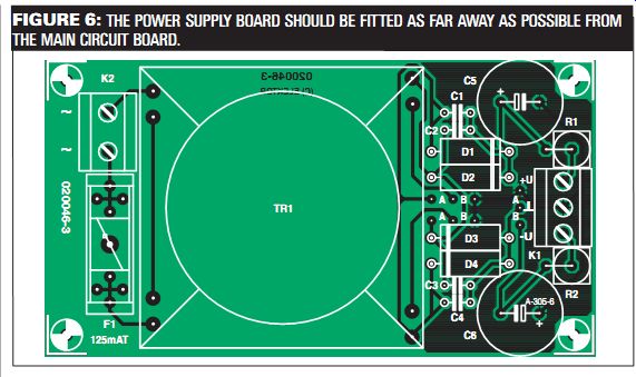
FIGURE 6: THE POWER SUPPLY BOARD SHOULD BE FITTED AS FAR AWAY AS POSSIBLE
FROM THE MAIN CIRCUIT BOARD.
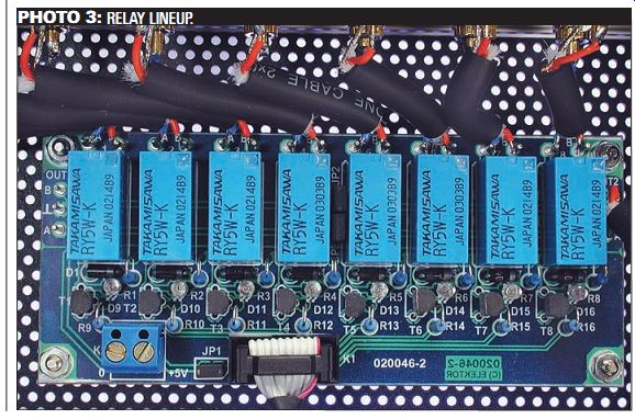
PHOTO 3: RELAY LINEUP.
TESTING, TESTING, TESTING ... AND INTO THE BOX
Before inserting the microcontroller and the PGA2311 into their sockets and connecting the display, you should painstakingly check all the boards for incorrectly fitted components, dubious solder joints and solder bridges. The first test should be performed with the boards outside of the enclosure. To hold the boards securely in place for testing,
screw them to the workbench using standoffs under each of the boards.
First connect the power supply boards and check the voltages at their outputs. Due to the high open-circuit voltage and the combination of rectification and filtering, the measured voltage will naturally be somewhat higher than the 7V specified for the transformer.
Next, connect all of the boards together and switch on the power.
Nothing will happen, but the following voltages should be present at the appropriate IC pins and the display module connector:
+5V:
K3-2, IC1-12, IC1-35, IC2-4, IC2-12
-5V: IC2-13
If everything is OK, wait a few minutes to allow the capacitors to discharge, and then insert the ICs and connect the display.
The display, the microcontroller, and the volume control IC are highly sensitive to static electricity. As all of these components are not exactly inexpensive, you should work at a suitably earthed workstation.
Figure 7 gives a deep insight into the laboratory prototype of the digitally controlled high-end preamp. The mains filter was fitted because it was "already on hand," but it is fully adequate. The power supply boards and the main board are separated as far as possible.
Nevertheless, the FFT analysis (see Part 1) shows that induced 50Hz noise is responsible for the majority of the distortion. If you want to improve matters and are not afraid of a bit of effort, you can fit the sensitive audio portion into a suitable tinplate enclosure.
At the rear, besides the mains input ...
-------------
COMPONENTS LIST
MAIN BOARD
Resistors R1 = 27? R2, R9 = 47 k-ohm R3 = 8-way 10 k-ohm SIL array R4 = 4-way 10 k-ohm SIL array R5 = 1 k-ohm5 R6, R7, R8, R10 = 10 k-ohm P1 = 10 k-ohm preset P2 = 100 ohm preset Capacitors C1, C2, C3 ,C20 = 10µF 25V radial C4-C11, C14, C15 = 100nF C12, C13 = 27pF C16, C17, C18 = 2200µF 25V radial C19 = 100nF ceramic, lead pitch 5mm Semiconductors D1 = low-current LED (+ 2-way pinheader)
D2, D3, D4 = zener diode 5V6, 1.3W IC1 = PIC18LF452-I/L (PLCC). Blank ICs: Farnell # 400-9654. Programmed ICs: order code 020046-41 IC2 = PGA2311PA from Texas Instruments/Burr Brown or CS3310 from Cirrus Logic (Crystal)
IC3 = SFH5110 (TSOP1836) (+ 3-way pinheader)
IC4, IC6 = 7805 IC5 = 7905 T1 = BC550C
Miscellaneous JP1, JP3 = 2-way pinheader + jumper JP2 = wire link K1 = 3-way PCB terminal block, lead pitch 5mm K2 = = 2-way PCB terminal block, lead pitch 5mm K3 = 16-way pinheader K4 = 10-way box-header, vertical K5 = 26-way boxheader, vertical X1 = 10MHz quartz crystal 12 solder pins External parts: LCD, 2 ×16 characters with backlight 12 pushbuttons for chassis mounting 2 Cinch sockets for chassis mounting, isolated and gold-plated Mains on/off switch, chassis mount IEC mains appliance socket, chassis mount Disk, hex and source code files, order code
020046-11 or Free Download.
RELAY BOARD
Resistors R1-8 = 10 k-ohm R9-R16 = 47 k-ohm Semiconductors D1-D8 = 1N4004 D9-D16 = low-current LED T1-T8 = BC550C
Miscellaneous JP1 = 2- way pinheader + jumper JP2, JP3 = wire link K1 = 10-way boxheader, vertical K2 = 2-way PCB terminal block, lead pitch 5mm RE1-RE8 = RY5W-K (Takamisawa), Conrad Electronics # 502852 (5V/167?) 16 Cinch sockets for chassis mounting, isolated and gold-plated COMPONENTS LIST PSU ASYMMETRICAL
Resistors R1 = 0.1 ohm 5W
Capacitors C1-C4 = 47nF, lead pitch 5mm C5 = 4700µF 25V radial, max. dia. 16mm
Semiconductors D1-D4 = BY500-200
-------------------------
Miscellaneous F1 = fuse, 125mA, slow, with PCB mount holder K1 = 2-way PCB terminal block, lead pitch 5mm K2 = 2-way PCB terminal block, lead pitch 7.5mm TR1 = mains transformer, 2 × 7V 10VA, low profile, e.g., Talema 70040 (RS Components, Digikey) Fit wire links "A" Do not mount R2, C6
SYMMETRICAL
Resistors R1, R2 = 0?1 5W Capacitors C1-C4 = 47nF C5, C6 = 4700µF 25V radial, max. dia. 16mm Semiconductors D1-D4 = BY500-200 Miscellaneous F1 = fuse, 125mA, slow, with PCB mount holder K1 = 3-way PCB terminal block, lead pitch 5mm K2 = 2-way PCB terminal block, lead pitch 7.5mm TR1 = mains transformer, 2×7V 10VA, low profile, e.g., Talema 70040 (RS Components, Digikey) Fit wire links 'B'
REFERENCES AND LITERATURE
1. www.fcl.fujitsu.com/en/products/relay/index.html.
2. www.talema.de
3. www.avtechpulse.com/appnote/techbrief9.
4. www.jdm.homepage.dk/newpic.htm.
5. http://jal.sourceforge.net.
6. http://groups.yahoo.com/group/jallist.
-------------
------------------
SOFTWARE MODIFICATIONS
Microcontroller programming is normally not the forté of audiophiles who have dedicated themselves to DIY construction. (Contact Elektor Electronics, sales@elektor-electronics.co.uk. regarding avail ability of microcontroller-order number 020046-41). However, any one who has a suitable development package for the PIC18LF452-I/L will certainly not have any problems downloading the hex code for the control program into the microcontroller (item number 020046 11, available at no charge from the Free Downloads page of the Elektor Electronics website http://www.elektor-electronics.co.uk/dl/ dl.htm). The easily constructed JDM programmer (see reference 4) is an example of a suitable programmer.
The software package also contains the source code, so interested users can get an idea of how it is constructed and/or make their own modifications (assuming they have suitable programming experience). The software is written in the JAL high-level language (see reference 5), which is available from the Internet as freeware. JAL is an excellent choice for getting started with PIC microcontroller programming, particularly since there are also very informative newsgroups on this subject (see reference 6). Nevertheless, it was necessary to make a few modifications to the JAL files in the assembly code since JAL does not provide native support for storing code in the EEPROM of the PIC18F452. All of the modified files are included in the project. If you wish to make changes to the source code, you should adjust the path names in the accompanying JAL.BAT file and use them for compiling. The software was compiled against JAL 0.4.59.Win32.
The software was entirely written by the author, except for a few functions such as driving the display, for which JAL provides native support. Functions such as the SPI interface code and acquiring RC5 signals were specifically developed for this project. Modification and/or reuse of parts of this software, including in your own projects, is explicitly desired, as long as the author is named and the software is used for non-commercial purposes (which means at home). More on this subject can be found in the file VV.JAL.
The PIC18LF452 can easily be programmed in-circuit. For serial in-circuit programming, a number of conditions must be satisfied: the PBGA2311 must be removed from its socket, and the connectors for the display and relay board must be disconnected. The programming interface comprises five connections: MCLR, RB6, RB7, +5V, and Ground. These connections are arranged in a row on the circuit board and fitted with solder pins.
---------------------------
... socket there are two sets of eight audio inputs and two audio outputs, all using isolated gold-plated Cinch sockets.
After the "official" completion of the device in the Elektor Electronics lab, further tinkering revealed that small RC networks on the inputs suppress induced RF noise on the cables, and that a 100 ohm series resistor in each of the output lines assures the stability of the PGA2311. As shown in Fig. 8, these components should be soldered directly to the Cinch sockets using the shortest possible leads, or even fitted in the connecting cable, in order to maintain the highest possible degree of screening.
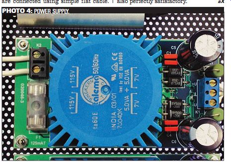
PHOTO 4: POWER SUPPLY.
In contrast to the audio connections, which employ high-quality twin screened cable, the keypad (which does not have a circuit board) and the front-panel LED are connected using simple flat cable.
This allows a relatively large amount of freedom in the layout of the front panel.
For example, the volume buttons can be arranged in a diamond pattern (if sufficient room is available). You can spare yourself the trouble of looking for a distributor for the attractive metal but tons used for the prototype-they were personally turned by the author.
The bright red cable between the main circuit board and the LC display came from a computer shop. But be careful: many of the cables available in such shops have crossed lead pairs. In case of doubt, a "normal" flat cable is also perfectly satisfactory.
============
Also see: