|
|
Continuing (from part 1) with the Error-Correction Amplifier amp design, covering the voltage amplifier and input buffer stages.
Okay, previously, I discussed the principle of error correction and developed an error-correction power output stage. Now, I will use H.ec in a voltage amplification stage and present the complete amplifier.
BACKGROUND
Let me back up to the conceptual circuit of error correction, as defined by Malcolm Hawksford, shown in Fig. 1A. You know that if the summers S1 and S2 are unity gain summers, you get Vout = Vin, an ideal gain-of-one amplifier stage. But for the voltage amplification stage (Vas) that drives the output stage, you need much more than unity gain.
Common amplifier gains are around 26 to 30dB, a gain of some 20 to 30 times. I like the lower value because it is better to have less gain in the power amp than to have a lot of unnecessary gain, only to need to turn down the volume control to get rid of it. It turns out you can use H.ec in voltage amplifiers quite easily if you insert an attenuator in the Vout sense leg, similar to what you would do in a regular negative feedback circuit.
I did that in Fig. 1B. The sums are slightly different: Vc = (Vout/Beta)-Ve, but still Ve = Vin-Vc. Substitution and rear ranging shows that now Vout/Vin = 1/Beta. So, if you make Beta, as is customary, from a simple resistive 1:20 voltage divider, you now have an amp with gain, linearized by error correction.
One other very important note:
When I found that the open-loop gain was no longer part of the amp transfer equation, I said that the gain of the amp block no longer had any bearing on the final result. That is true in theory, but not in practice.
In the case of the power output stage, I said the gain is “about 1.” A realistic value would be 0.98 at mid frequencies and light load, down to 0.95 at higher frequencies and higher loads. That means that the error-correction circuit needs to add 0.02 to 0.05 times the signal level to the input to straighten out the amp. Intuitively, I believe it is advantageous to have only small signals in the error-correction circuitry that helps it to work linear and with low distortion.
But in the case of the Vas, if the for ward gain block has only a gain of 1, the error-correction circuit will need to add 19 times the signal level, and it would be much more difficult to design simple circuits that could handle those levels with high linearity. So, what you need is to make the open-loop gain of the Vas amplifier block such that the signal levels in the error-correction circuit are minimized. This will be the case when the open-loop gain is as close as possible I to the closed-loop gain. Then, there will be quite small differences between the input of the actual amplifier and the scaled-down output (by Beta), and that small difference then is the error signal.
This, of course, is totally at odds with what you would do for a negative feedback amp. There, you would try to get the highest open-loop gain you can get away with, stability wise, to have a lot of excess gain for the feedback loop to work with. Not so with H.ec, and a corollary to this is that your Vas can now be a very simple gain-of-20 amp.
VOLTAGE AMPLIFIER
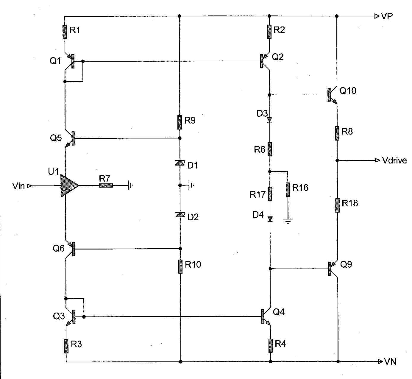
The particular topology I chose is in Fig. 2. It’s very simple. U1 is a unity-gain buffer. Vin applied appears at the buffer output across R7.
The output current through R7 comes from the supplies, of course, so you find a signal current Vin/R7 in the current mirrors formed by Q1 and Q3. The DC quiescent current for the buffer (I’ll tell you later which buffer type I used) happens to be about 7mA. With an R7 value of 220-ohm and a current of 14mA peak-to-peak available, this buffer can handle a little over 3V peak (about 2V RMS) before running out of class-A, which, of course, is good for linearity. With an amplifier gain of 20 that is enough to deliver 100W in 8-ohm.
That same signal current in Q1, Q3 is mirrored through Q2, Q4 and flows through R16 to generate the output voltage. As a first approximation, because the same signal current flows through R7 and R16, and the signal across R7 is the same as Vin, the gain (open loop) of this circuit is simply R16/R7, which is about 20 times. So, this is the Vas stage.
But in Part 1 I said that the amplifier output stage needs to be driven by a low (and constant) source impedance (ideally zero Zsource) for the output stage H.ec to work; so add a low output impedance emitter-follower stage to the basic Vas stage (Q10, Q9). This emitter-follower stage is also biased at about 7mA. If the voltage across D3 is equal to Vbe of O10, the voltage drop across R6 and RS will be the same, so if you chose R6 = R8, the same current that is flowing through Q2, Q4 will also flow through Q10, Q9. In practice, the diode voltage and Vbe don’t exactly match, so make R6 slightly smaller than R8. D3 and D4 provide a measure of temperature stabilization to the emitter-follower output stage bias current.

FIGURE 1A Basic H.ec topology for gain-of-i stage
FIGURE 1B: Arbitrary gain stage.
Now that you have the main gain block for the Vas, enclose it in an error-correction loop as you did with the output stage (Fig. 3). Note here, that, first, although both the EC sense and the EC generation resistors are given as “R,” they are not equal. The sense resistance value at the right is the sum of resistor R plus the output resistance of the Beta-network (R11//R12). It is the total resistance of R plus R11//R12 that determines the error current into the CCII. That same current generates the EC voltage when flowing through the left side R, and these voltages should be equal, so similarly, the left side “R” is actually the series resistance of the nominal R and the output resistance of whatever Vin source will drive the Vas. I’ll come back to this issue later.
Second, note that the gain of this amp is not strictly 1/Beta. Terminal Y is a virtual earth point. To calculate the exact attenuation from Vout to the node R11, R12 and R, you need to account for the fact that for the attenuation, seen from the Vas output Vdrive, R appears in parallel with R. So, the attenuation, and thus the gain, is slightly higher than 1/Beta.
You need to consider both of these issues when you dimension the error- correction sense and generation resistors. Just as with the output stage, I use an AD 844 current conveyor for the EC circuit, while the buffer is used in the amplifier input stage to drive R7. The complete Vas circuit is shown in Fig. 4.
I have yet to mention the diodes D9, D12, D13, and D14. What happens if you overdrive the amp? The positive feedback loop is regenerative and will continue to increase the input signal until stopped by some physical limit such as the supply voltage or current or voltage limitations in the circuit. In the Vas stage, this is limited by the four di odes across the error-correction generation resistor R29 (Fig. 4).
When the amp is overdriven, the error correction current out of pin 5 of the AD844 CCII will increase considerably. This current will start to generate a large correction voltage across R29, to the point where the threshold voltage of the diodes is reached. At that point, the effective impedance of R29 collapses to just the dynamic diode impedance that is only a few tens of ohms. Further increases in the error—correction current will not generate more error-correction voltage and the positive feedback loop is broken. This makes the clipping clean and recovery fast. But you run the risk that the diodes increase the distortion because they may already con duct small current before the threshold, which would upset the error-correction accuracy.
It turns out that because of the very small error-correction voltages across R29, this can be avoided. In Fig. 6 you see that if you use a single pair of soft clipping diodes, the distortion starts to rise before maximum output. With the dual pairs, no difference is apparent.
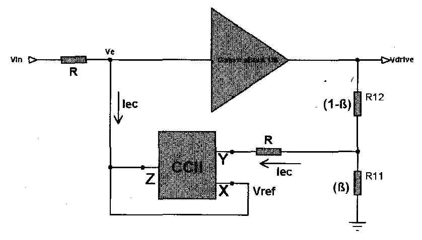
FIGURE 3: The CCII as the H.ec element for the Vas stage.
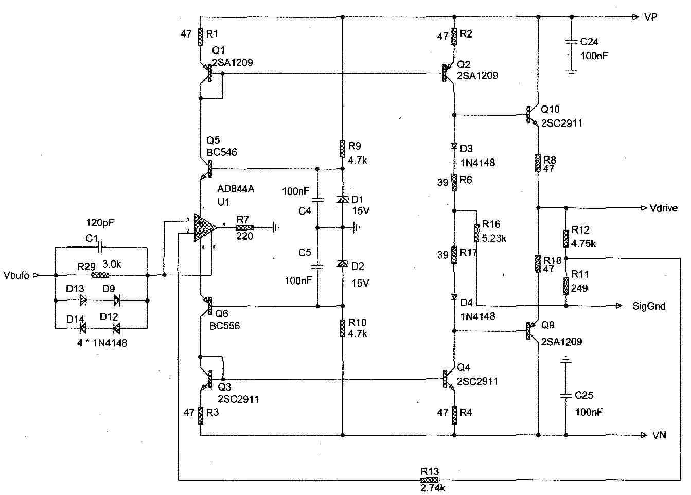
FIGURE 4: Full circuit of H.ec and Vas stage.
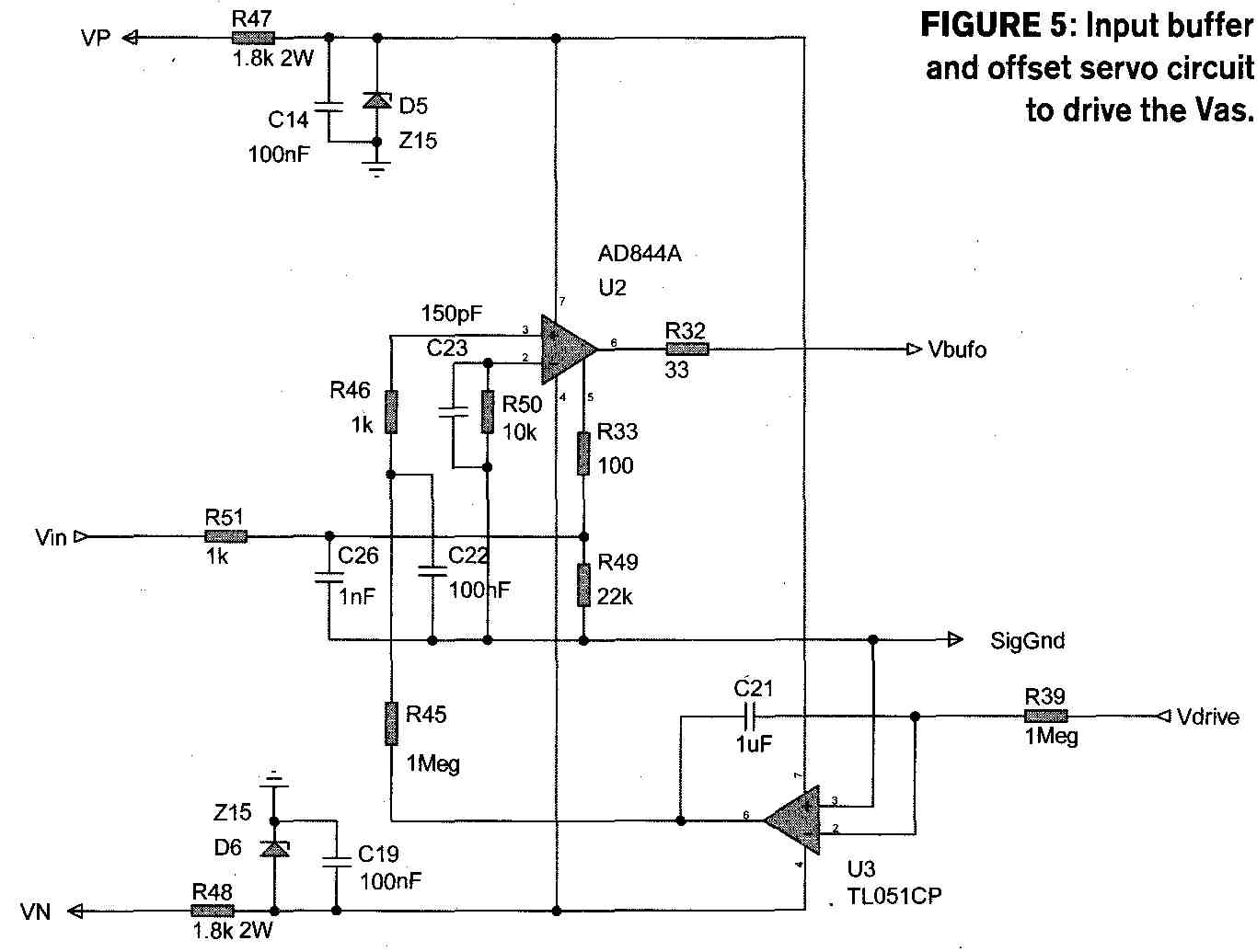
FIGURE 5: Input buffer and offset servo circuit to drive the Vas.
Figure 7 shows this effect from a different perspective. The soft clipping diodes for the negative signal part have been temporarily removed so only the positive signal is affected. You can see that without the diodes, clipping recovery is delayed (negative part), while with the diodes (positive part), there is only a hint of delay.
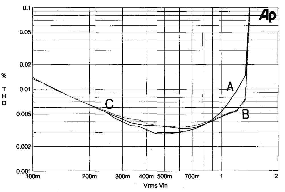 FIGURE 6: Amp distortion as a function of output level, with single diode
(A), dual diode (B), and without soft-clipper diodes (C).
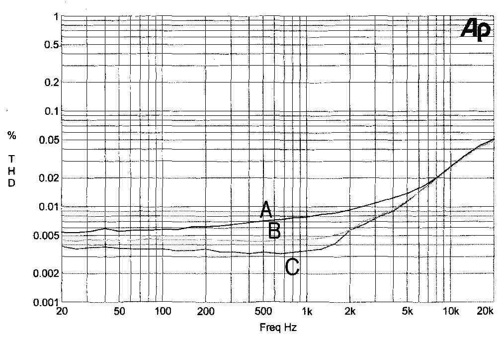
FIGURE 7: Amplifier distortion vs. frequency at 50W in 8 with single diode
soft clipper (A), dual diode soft clipper (B), no soft clipper (C).
BUFFER STAGE AND DC OFFSET
All that is needed now for a complete amplifier is the input buffer and the DC offset servo (Fig. 5). Just as with the output stage, you need to drive the Vas input resistor, which develops the EC voltage (R29), with a low impedance source. You guessed it: I will again call upon the open-loop buffer in an AD844 to drive the Vas from Vin. The signal enters the buffer in U2 through R51 and R33 at pin 5 and exits at pin 6.
The enemy of your speakers (and the amp as well) is DC offset at the output terminal. Most amps have some sort of means to avoid that. In this amplifier, the output stage itself doesn’t need any additional measures: the error correction ideally duplicates the driving voltage (from the Vas) to the output terminal, with zero offset, although there will still be some offset of a few millivolts from the error-correcting AD844. The only requirement is that the Vas has negligible DC offset.
The Vas, however, has higher gain and will amplify its own AD 844 offset with that gain. I decided to implement a DC servo to keep the Vas offset under control. The servo uses a standard low-offset opamp, a TL051CP. I will use the uncommitted current conveyor in that input AD844 (U2, Fig. 5) to couple the servo signal to the amplifier.
The way this works is as follows: Remember that whatever current flows in or out of the low impedance input pin 2, also flows (in opposite direction) out of or into pin 5. You also know that the voltage at pin 2 and 3 will track accurately. When you couple the servo signal to the reference input pin 3, it will cause a current in R50 to keep pin 2 at the same level. That same current will flow in R33, and in this way the offset correction will be added to Vin.
R49 ensures that that current, which essentially is DC, can flow in R33 even if the Vin comes from a coupling capacitor.
Finally, this input buffer and servo amp have their own ±15V supply from two zeners, D5 and D6. With this circuit, compound offset of the whole amp is just a few millivolts.
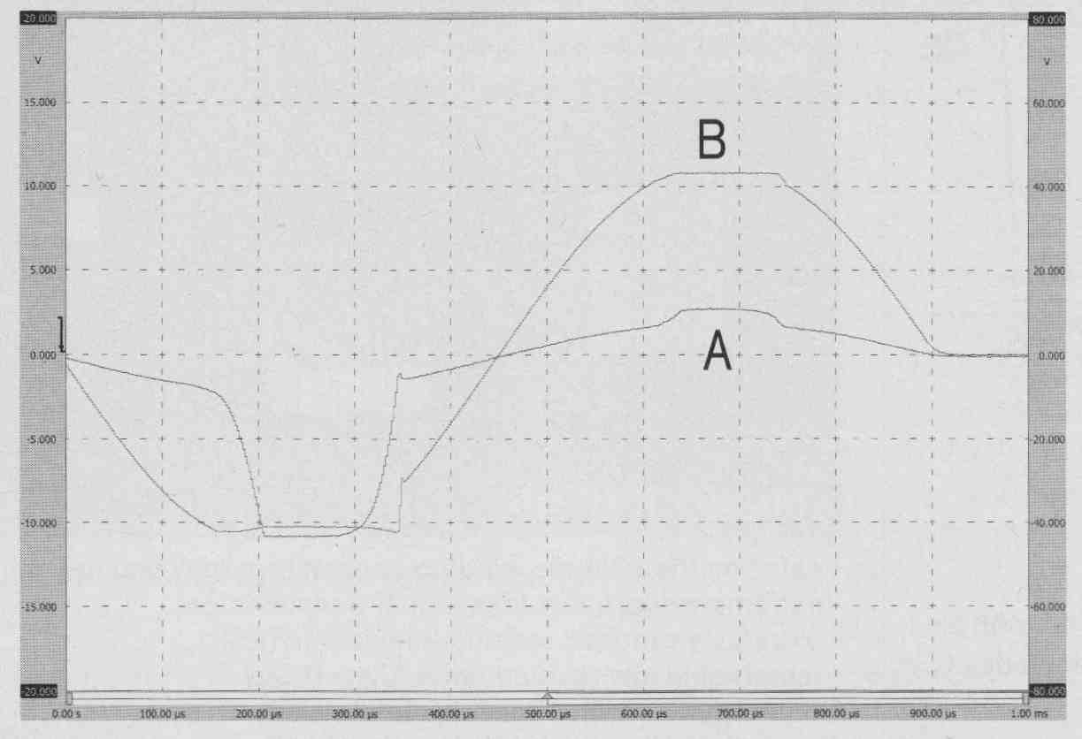 FIGURE 8: Error-correction current (A) and amplifier output clipping (B)
with soft clip per (positive signal) and without soft clipper (negative signal).
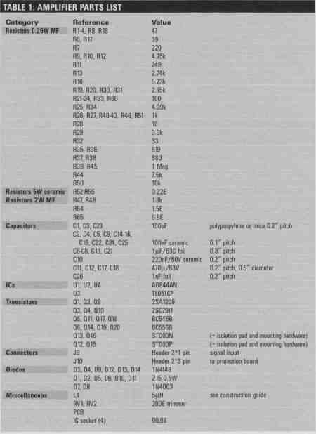
---- Table 1: Amplifier parts list ----
POWER SUPPLY
The power supply for this amp should deliver about 2 x 42V DC. Although the output devices are rated for higher voltages, it is not advisable to increase the supply in trying to achieve more output power. The allowed dissipation at higher Vce is much less than the rated DC dissipation due to secondary breakdown limitations of the SOA (Safe Operation Area). With loads that dip substantially below 4-ohm, even temporarily, the SOA may be exceeded and an output Darlington destroyed. The supply for the error- correction circuit in the output stage is bootstrapped from the output; that part of the circuit can actually drive the output devices beyond the supply voltage.
Consequently, it is the Vas that determines how close the output can get to the supply rails. Because the Vas will clip first, there is no clip ping overdrive and overdrive delay in the output stage. The output can swing within a few volts of the sup ply, which is better than in most amps (unless you use separate higher voltage Vas supplies).
The power supply is uncritical. The error correction not only corrects internal amp nonlinearities, but also any power supply ripple or noise that makes it into the circuits. (The sup plies for the error-correction AD844s are stabilized separately with zener di odes.) Therefore, a classic rectifier-and- reservoir capacitor supply delivering 2 * 42V DC under load is sufficient for about 100W in 8ohm 200W in 4ohm.
The power supply circuit details are given in Figs. 9 and 10. For a stereo version, a 300 or 400VA transformer should be sufficient; after all, you will not drive both channels at full power for a long period (except maybe on the test bench). You can use the common transformer with a center-tapped secondary, but you can use other con figurations.
One nice option for a stereo amp is to use two completely separated sup plies, each with a 250 or 300 VA transformer. Completely separated supplies for each channel make it easier to maintain strict star grounding.
It is important .to get the grounding right. Ground currents back to the supply from the speaker, as well as from the reservoir caps, can be quite large and have all kinds of ripple and noise. Such ground currents generate voltages across the ground return wiring. If the ground for the signal is connected to this ground wire at another point, you have effectively produced a small ripple signal that appears in series with the input signal. This may seem far-fetched, but with very low distortion and very clean amplifiers, even a few mV of these noise signals can be enough to ruin the linearity and distortion figures of an otherwise very good amplifier.
Usually you try to prevent this by using a star ground: All ground re turns come together at a single point, and no signal return runs through the same ground wire with another return loop. The power connections to the PCB also get to a central star point. On the P itself, I’ve tried to maintain this. There are two or three separate traces that bring the returns for the regulator zeners and the de coupling capacitors to the same point.
The signal returns from the input network, the gain setting resistors R7, R16, and the attenuation network R11, R12 are brought to a separate point. All return wires from the sup ply, the transformer, and the speaker are returned to this point, the star ground.

FIGURE 9: Mains wiring for the power supply, mains filter, over-voltage clamp,
and fuse.
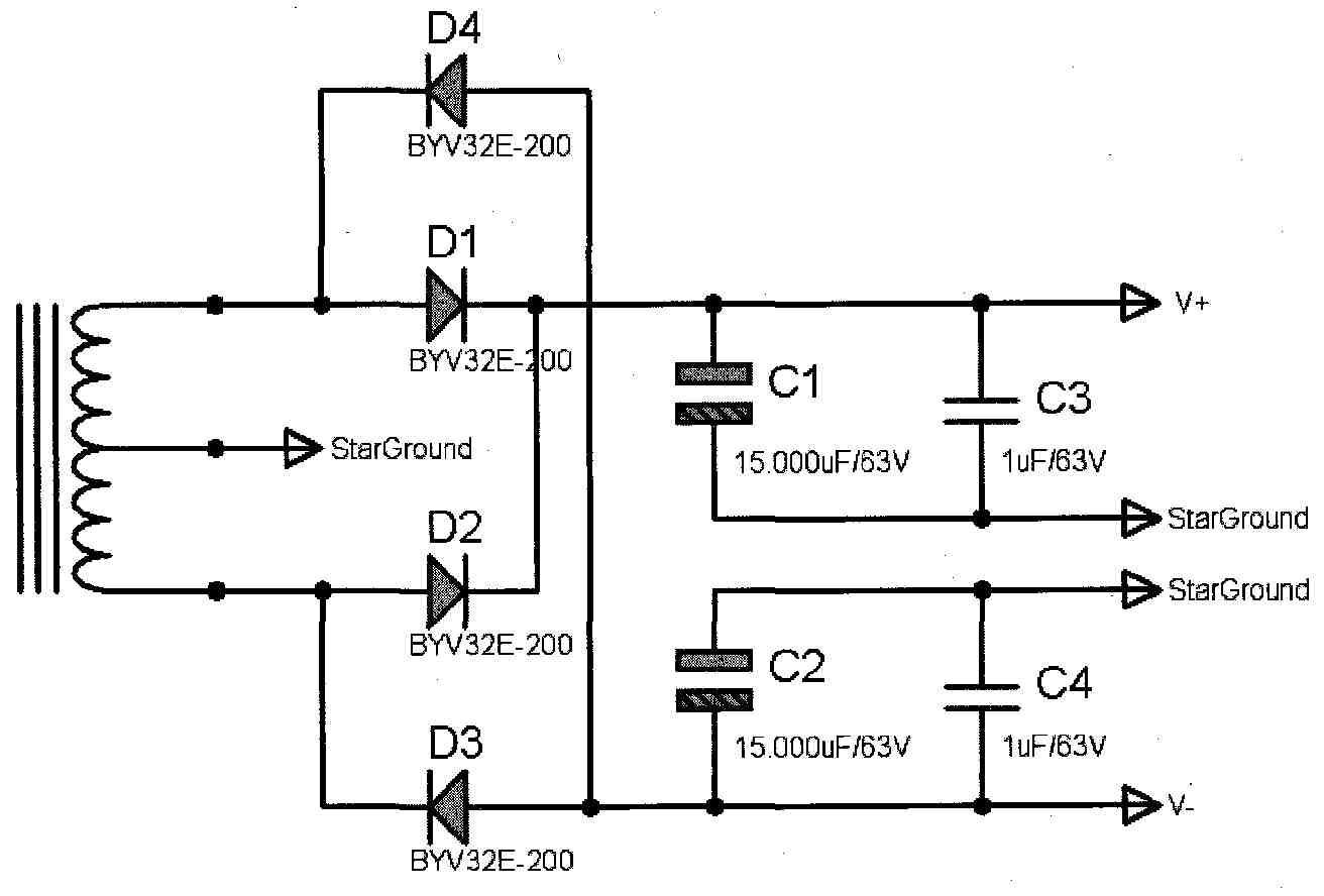
FIGURE 10: DC power supply. Diodes are paralleled, dual, fast, soft recovery
3-pin TO-220 types.
The signal grounds are returned to this point via a low-value resistor R28, which is then by definition the “clean” ground point (pad J1 on the PCB is the clean ground and should be used as “ground” for measurements as well). Any error voltages generated by ripple and pulsating currents in the ground wires cannot end up in the signal, except through radiation. In turn, you can minimize this by making all high-current wires short and as far away from sensitive signal areas as possible.
Finally, the rectifier diodes should be types that recover quickly from voltage reversal when switching off, and do so “softly”—that is, without very sharp current steps. Diodes that take a long time to reverse themselves and in the process generate sharp current steps may cause high-frequency noise that is difficult to filter out. Fast, soft recovery types don’t need capacitors or snubbers; indeed, such capacitors would only increase the transmission of mains-borne noise to the amplifier.
I recommend you use Philips BYV32E-200 diodes, which are TO-220 dual types with a common cathode; the two diodes should be paralleled. They have a relatively small threshold voltage, and are quite inexpensive. They don’t need to be heatsinked, so you can put them on a PCB in free air. For the reservoir capacitors, you should use a minimum of 15,000uF per supply polarity. 63V rating is adequate.
You should use a mains filter (Fig. 10) to keep out high-frequency noise and switching pulses riding on the mains. Good mains filters are not cheap but worthwhile; use a type with at least 12A rating for US (120V) mains. Ground the filter ground lug as well as the mains safety ground wire to the chassis only. Use a slow-blow fuse of 6.3A for a stereo version, larger if you use larger reservoir capacitors. A 150V AC varistor clamps any high-level pulses that make it out of the filter.
IN CONCLUSION
So, there you have it, a complete, high- quality yet simple error-correction power amp. A complete parts list is in Table 1. Although harmonic distortion measurements do not always correlate with sound quality, they do give an indication of linearity and behavior of an amplifier. Therefore, a few performance curves are given in Figs. 7 and 8.
If you want to build this amp, there is a detailed audioXpress .com/files/didden3038guide.pdf">Construction Guide for the amp on the web. Working step-by-step, checking your work after each major part will help to avoid errors and, if errors are made, to quickly isolate and fix them. Also check on my website for any last-minute in formation, additions, or corrections.
This is not a very difficult project, but will give you an excellent amplifier, which reproduces your source music faithfully—adding nothing, taking nothing away. This amplifier is stable and will happily drive a wide range of different speakers. In short, an amplifier that will let you enjoy your music for many years to come!
Further reading:
A MOSFET Power Amplifier with Error Correction, Robert R. Cordell, Journal of the Audio Eng. Soc., Vol.32, No.1/2, 1984 January/February.
