This small phono preamp design by a noted author solves several problems
inherent in today's audio systems.
by Norman E. Thagard, NASA Astronaut and DIYer
While I have designed and constructed several audio power amplifiers in the past 12 years, I have never, until recently, done much preamplifier work. I have considered attempting to design and con struct a preamplifier for several years, but I find I am usually prompted to begin a project by need, rather than intent. That is true of the phonograph preamplifier I de scribe here.
THE NEED ARISES
Unlike some audio purists, I have been very interested in surround sound since the early '70s. With the incorporation of my sound system into an audio/video system, I replaced my Krell preamplifier first by an Adcom and then by a Marantz A/V tuner/preamplifier. Unfortunately, as with most modern units, neither the Adcom nor the Marantz had a phono input. Lately, the Krell has functioned solely as a pre-preamplifier, that is, as an interface between the phono cartridge and a high level (Tape 1) input on the Adcom.
Having a bulky preamplifier in the system was undesirable, however, because I had no more room for additional components in the equipment rack. I wished to replace the Krell with a dedicated small phono preamp that I could locate behind the equipment rack.
It occurred to me that I was probably not the only one who might need a stand alone phono preamplifier that would allow updating the system preamp with out losing the phono option. Thus I finally developed the impetus to attempt the design of at least one component of a pre amp, the phono stage.
The design I present here allows the phono cartridge to appear as a high-level source that you can input into any of the standard, flat-response, high-level inputs on an audio or audio/video preamp or receiver. The few purists left will appreciate the irony of using the CD input, as I do with the Marantz. The CD input circuitry in my 1985-vintage Krell PAM-5 manipulates the signal in some way-perhaps to compensate for the interchannel time difference in early CD players-so a tape or auxiliary input might be better in some cases.
I specifically designed this preamp for moving-magnet cartridges capable of at least a couple of millivolts output at 1kHz. With some minor changes, you could probably use it with a moving-coil cartridge whose output was 20dB less. I make no claims for this, however, because I did not examine the possibility.
EQUALIZATION
The principles of preamplifier design do not differ greatly from those of amplifier design, the major differences being power and noise considerations. The exceptions are for preamps intended for tape heads and phono cartridges. The cartridge requires not only more amplification (because its output is significantly lower than, say, a CD player), but also equalization.
Equalization involves tailoring the frequency response of the preamplifier in a manner that exactly compensates for the frequency response of the signal at the input. The idea is that the overall frequency response will be "flat" in the sense that the original spectrum of the sound is maintained in reproduction.
---------------
About the Author
Five-time astronaut Norman Thagard was the first American to enter space aboard a Russian rocket for a 90 day mission to the space station Mir. With a total of 140 days in space, he became the most experienced US astronaut ever. In addition to an MS degree in engineering science from Florida State University, he holds a doctor ate in medicine from the University of Texas Southwestern Medical School. Dr. Thagard is currently Professor and Director of College Relations at the FAMU-FSU College of Engineering. An avid audiophile, he designs and builds audio amplifiers as a hobby.
---------------
The frequency shaping that must take place in the phono preamp is that of the RIAA curve. This curve has been the basis of several previous articles in Audio Amateur, so I do not intend to be overly repetitious. I have liberally footnoted this article with references that contain addition al information for the reader who seeks more details.
I shall be slightly repetitious in reminding you that the equalization is required because neither the recording nor the cartridge response is flat. To avoid overly wide groove excursions on the record, the low-frequency components are com pressed, while, to improve signal to-noise ratio, the high frequencies are emphasized. [1] On the reproduction side, a magnetic cartridge is a velocity-responding device.
If groove amplitude were held constant, electrical output would be proportional to frequency. To compensate for these factors, response is boosted by a factor of about ten (19.3dB) at the low end and attenuated by roughly the same factor at the high end (19.6dB), where 1kHz is the reference (0dB) frequency.
CURVE-SHAPING POLES
Suffice it to say that there are two poles, one at 50Hz and the other at 2k122Hz, as well as a zero at 500Hz, that shape the curve. There are many different ways to produce these poles and the zero, with different designers favoring different schemes. The most economical method uses negative feedback around only one gain block, with the feedback network made frequency-dependent by adding two capacitors and one resistor to the usual passive voltage-divider feedback network.
You can easily accomplish single-ended designs with just two bipolar junction transistors (BJTs) per channel.
Since closed-loop gain is approximately equal to 1/ß, where ß is the fraction of the output fed back to the input, it follows that a zero in ß (i.e., a feedback zero) produces a closed-loop-gain pole, and a feed back pole produces a closed-loop-gain zero. Thus, there are two feedback zeroes and a feedback pole at the frequencies corresponding to the RIAA poles and zero, respectively.
Achieving great accuracy in RIAA curve tracking with this method is more problematical, because the components in the complex RC feedback network interact. [2] It is not a simple case of calculating the three breakpoints as independent RC time constants. Mathematically, there are cross-product terms in addition to the terms of interest. Then, too, if the amplifier is noninverting, the closed-loop-gain rolloff due to the feedback zero at 2k122Hz cannot be sustained, because this gain cannot drop below unity. In effect, an unintended zero is added to the response at some higher frequency.
While you can eliminate this latter defect with an inverting configuration, the ubiquitous 47k moving-magnet loading resistor winds up in series with the cartridge's own DC resistance instead of in parallel with it. The upshot of this is that the considerable noise generated by this resistor is input into the preamp rather than being largely shunted to ground through the source resistance of the cartridge, as it is in the noninverting configuration.
DESIGN PHILOSOPHY
You can find a discussion of the topics of the last paragraph and the philosophy upon which the design described in this article is based in National Semiconductor Applications Note AN 346. [3] This design largely obviates the problems to which I've alluded. Previous articles in TAA or AE have offered designs based on this same philosophy. Since that is the case, it is valid to ask why I offer yet an other similar design. The answer is that I desired to implement a discrete version of the op-amp-based design from AN346.
It is a good challenge because the AN346 design used two op amps. Seeking op amp performance with discrete components can involve a lot of parts, and implementing two such amplifiers in discrete form means yet another such group of parts. Near-op-amp parameters are, in fact, required because high input impedance, low output impedance, and high open-loop gain are crucial to proper performance of the circuit.
As an engineering professor, I receive textbooks for evaluation from time to time. One of these described a one-stage op amp, [4] realized by using the folded-cascode topology. It could be argued that a cascode, folded or telescopic, is really two stages. However, from the standpoint of audio-frequency performance, a cascode has all the earmarks of a single, albeit compound, stage. It behaves like a "super" common emitter or common source stage with higher bandwidth and lower distortion.
I have had a predilection for cascoded stages ever since reading an article on the subject by Nelson Pass. [5] My very first amplifier design was a 100W Class A (at 8 ohm) DC monoblock that featured four telescopically cascoded stages, including the power output stage. [6] In 1992 I designed and constructed a balanced-input amplifier that featured a MOSFET-based differential-in, single ended-out folded cascode very similar to the phono preamplifier described here.
That design permitted a CMRR >60dB at 20kHz and will be the subject of a future AE article. Finally, the Thagard/Pass A75, the design of which was completely Nelson's, but which incorporated some topo logical features that I had suggested, offered the option of a folded cascode. [7]
COMPLEMENTARY SYMMETRY
In the current application, using a folded cascode in complementary symmetry results in sufficiently high open-loop gain, since the drain of each common-gate device "sees" the drain of its complementary partner as its load device. From the diff-amp input to the single-ended output, gain is given by ½ g_m R_load, where gm is transconductance and Rload is the load resistance.
If Rload is the intrinsic resistance (call it Ro) looking into a JFET drain, then the gain is very high, because Ro often ranges from 100k to 1M. Of course, the caveat is that the input of the feedback network does not load the output node, and that is not a good assumption here. Similarly, the following stage must not load the output node, either, and that is a reasonable assumption here. Apparently, the JFET transconductances are high enough to en sure that the open-loop gain is also sufficiently high.
I began with the intention of using the LM394 BJT "superbeta" monolithic matched pair in the diff amp. JFETs typically have a transconductance that is an order of magnitude smaller than that of a BJT in a given application. Also, the source resistance of a moving-magnet phono cartridge is seldom more than about 1k, so that a low-noise BJT such as the LM394 actually has an advantage from the standpoint of noise. [8] The lower transconductance of most small-signal JFETs significantly adds to their noise voltage output. [9] The JFETs used in this design have values of g closer to those seen in similar BJTs, so the LM394 noise advantage will be less. An other entry on the negative side is that the input-voltage offsets and drifts are higher in JFETs. The interelectrode capacitances are higher in JFETs, too, but the cascode largely obviates this negative aspect.
It was Erno Borbely's article describing the 2SK389/2SJ109 high-transconductance complementary monolithic pair JFETs that changed my mind. [10] For one thing, I was aware of no pnp equivalent to the LM394. For another, the BJT input resistance is much smaller than that of the JFET, although the LM394's high beta does result in a respectable resistance.
Thus, this design is mostly a JFET one.
It is entirely JFET-based, if you accept the notion that the BJT active-load devices aren't really in the signal path. I believe that this is valid, since, ideally, no signal currents could pass through these devices.
NOISE
I have never given much thought to noise in my power amplifier designs. Indeed, there was little reason to do so for a gain of-twenty amplifier that requires an input of around 1V in order to produce full power output. This is why one of my designs uses MOSFETs in the input diff amp. No one can make a good case for low-noise operation of the MOSFETs that would be used in a power amplifier. [11] Low-noise operation is a major consideration in designing a preamplifier for moving-magnet cartridges. Gain at 1kHz is around 38dB, and the input signal might be about 5mV at best, depending on the cartridge. The output will be boosted by another 20dB in the line-level preamplifier stage and a final 26dB by the power amplifier. This is a total amplification of almost 16,000. Signal or not, any noise at the input is amplified by this factor, which is why even my Krell has some audible noise in the phono position if your ear is close enough to the loudspeaker.
It should be obvious that the first stage in this chain is the most critical from the standpoint of noise. Paralleling devices reduces noise, so the complementary nature of the circuit helps, since the p- and n-channel devices are in parallel as far as the signal is concerned. [12] Unfortunately, a diff-amp stage has 3dB more voltage noise than a single-ended stage, and the two effects cancel. [13] It may come as a surprise to know that the biggest contributor to noise in a well designed phono preamp is the Johnson noise generated by the DC resistance of the cartridge itself. For the V15 Type V MR that I use, this resistance is 1k, for a contribution of about 4nV/vHz. According to the PSpice model of the circuit of this article, total input noise (all noise is, by convention, referred to the input) is little more than 5nV/vHz at most frequencies in the audio band.
If the model is correct, the preamp it self adds little to the total noise output. Although at the time of this writing I have made no noise measurements, listening indicates that noise is inaudible unless the ear is positioned immediately in front of the high-frequency drivers of the loud speakers.
RADIO-FREQUENCY INTERFERENCE
Figure 1 is the schematic of the preamp.
Starting naturally at the input, a series inductor stands out prominently. You just do not encounter inductors all that much in audio-frequency design. I had no intention at the outset to use this inductor.
However, while doing listening tests during the breadboard stage, I heard not only the record that was playing, but a local radio station as well. I remembered a reference to this possibility. [14] I used the solution suggested in the reference, namely the addition of a 10mH rf choke.
A side effect of using the choke is a slight rise in high-frequency response that causes an RIAA tracking error of about 0.1dB at 20kHz. This rise is due to the interaction between the input capacitance and the inductor. It is possible, of course, to lower the 2k122Hz pole to increase the 20kHz attenuation and thereby eliminate the induced error at 20kHz. I doubt that it is worth the effort.
You can omit the choke if you wish.
For compactness, I ordered a choke with a DC resistance of nearly 100. This resistance is in series with the DC resistance of the phono cartridge and will add to the input noise. There are coils available with much smaller resistances-for example, the M5942 from Digi-Key at 7.30 ohm. This coil is significantly larger, though, and will be difficult to accommodate if you use the PC-board pattern of Fig. 2.
Since a designer need design only to the interface conditions specified by the cartridge manufacturer, I have not been motivated to research the subject, but I have the impression from articles and from cartridge manufacturer-recommended capacitance values that the frequency response of a moving-magnet cartridge is, by design, extended by the resonance of the cartridge's intrinsic inductance with any capacitance in the preamplifier input circuit. If so, this is similar to the "peaking" that is sometimes used in rf circuits to postpone high-frequency rolloff. [15] The inductance of my cartridge is 425mH, so if peaking is already intention ally used, adding approximately 2% to the cartridge's own inductance may well be less than the variation in intrinsic inductance from cartridge to cartridge. It would not then be reasonable to seek such accuracy in an area where other uncertainties exceed the likely gain.
Since the recommended load conditions for the V15 Type V MR are 47k in parallel with 250pF, I added 100pF in the form of C1. That is because I use an SME 3009 Series II tonearm with 135pF of cable capacitance, and the preamp has about 80pF of intrinsic input capacitance by measurement, or 40pF according to the PSpice version of the circuit.
Even though 100pF is a bit higher than the calculated optimum, I thought that this was probably a good all-around value.
You are free to alter the value of C1 for the particular cartridge at hand. Frequency response suffers, however, if there is too much deviation from the recommendation for the particular cartridge used.
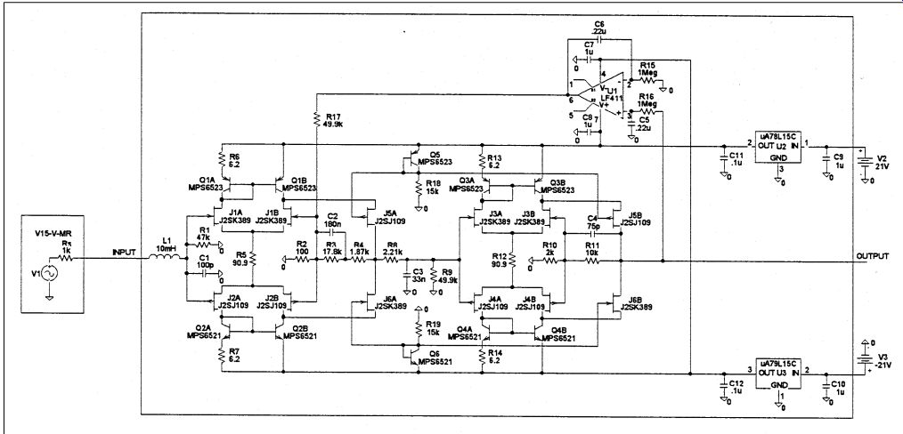
FIGURE 1: Preamp schematic.
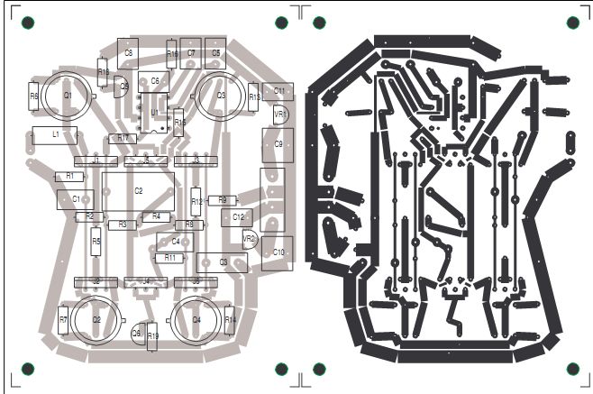
FIGURE 2: Preamp board parts placement (left) and PCB pattern (right).
TOPOLOGY
The input stage is a dual or complementary differential amplifier. I had hoped that the diff amp input would provide sufficient thermal stability to allow a true DC design. However, to find the zero tempco of the JFETs requires a knowledge of their pinch-off voltages. [16] Since this parameter varies from transistor to transistor, it isn't practical to base this design on the zero tempco. Although I was able to unbalance the diff amp to achieve zero-output offset voltage, the drift was excessive.
In the end, I adopted the same DC servo used by many others before me. [17] Even a venerable old µA741 op amp in the servo gave an acceptably low DC-output offset and drift. However, I accede to the almost universal use of the LF411 in specifying that part for this application. Certainly, the LF411 is a good choice, since it is sold as a low-offset, low-drift component.
On the breadboard, the LF411 required bypass capacitors near its power supply pins, even though the supply rails were al ready bypassed at the point of entry onto the board. That is why there are two bypass capacitors on the supply rails, one at the output of each voltage regulator and another near pins 4 and 7 of the LF411. You are welcome to experiment with eliminating the pin-4 and pin-7 capacitors. I included them on the prototype as a conservative measure. The µA741 did not require additional bypassing.
Be aware that the PSpice model showed considerable low-frequency distortion because of the servo. Increasing the integrator and low-pass-filter time constants corrected this problem in the model. Since I saw no such distortion in the breadboarded circuit, I left the components at the same 1M ohm/220nF values that I have seen used in other designs. However, feel free to increase the time constant by increasing the value of C to 1.0 or even 2200nF. PSpice permits perfect device matching, so the simulated DC-coupled, servo-less circuit had almost no DC-output offset or drift, facilitating the determination that the apparent problem was with the servo.
J-FET SELF-BIASING
As with vacuum tubes, you can use self-biasing with JFETs. That is the function of resistors R5 and R12. The target drain current was 3mA, meaning that 6mA should flow through those resistors. At 3mA, the JFET characteristic curves I ob served on a curve tracer suggested that:
Delta VGS = 0.27V was required.
With R5 = R12 = 90.9 ohm, about 0.55V source-to-source will be dropped.
Since the DC gate voltages are fixed at ground potential, the desired VGS for both n- and p-channel devices is attained, and, consequently, the desired drain currents are realized. JFET characteristics can vary, so if you determine that the drain currents differ greatly from the design value, simply change the value of R5 and/or R12 until VR5/R5 - =VR12/R12 =6mA. Of course, increasing these resistor values decreases drain current.
The right-hand diff-amp devices J1B, J2B, J3B, and J4B are the common-source halves of a cascode. The more traditional cascode, originally constructed from vacuum tubes, is now sometimes called a telescopic cascode to distinguish it from the folded cascode. The latter "folds" the cascode over toward the opposite voltage rail by using a device for the common-gate half of the compound stage that is complementary to the common-source device.
There were no complementary vacuum tubes, so it took the advent of the transistor before a folded cascode could be physically realized. It has the advantage of al lowing the cascode output to be at 0V DC with proper biasing. It facilitates the construction of single-stage opamps and, in discrete form, is the basis for the current design.
The folded cascode allows some flexibility in setting bias current in the common-gate device. This flexibility does not exist in the telescopic cascode, since the drain current is necessarily the same in both halves of the stage. There are reasons for setting folded-cascode common gate device bias at various levels depending upon the design considerations. [18] For simplicity and noise considerations, I elected to bias the common-gate devices at the same DC drain current as the common-source devices.
Each of the four dual BJTs, Q1-Q4, is configured as a kind of "reverse" Widlar current mirror in order to establish the bias currents for the common-gate devices in the cascode. Again, it should not matter that BJTs are used in this capacity rather than JFETs, since the whole idea of a current mirror is to pass as little signal current as possible.
Some shun the use of active loads in preamplifier and amplifier designs even for folded-cascode biasing. The reason, at least in some cases, seems to be a claimed adverse sonic effect. I am skeptical that any such effect exists except as a perceptual alteration induced by knowledge of the material to which you are listening. I prefer to use active loads be cause they ensure balanced diff-amp operation and, consequently, potentially lower distortion than you could obtain with simple resistor loads. [19]
COLLECTOR CURRENT
In discrete design, it is easier to establish a given bias current with a BJT-based Widlar mirror than with a scheme involving JFETs or MOSFETs. In BJTs, it is really base-emitter voltage that sets collector current. That is why the current ratio between the transistors in each half of each of the four mirrors is established by the difference in base-emitter voltages of those two transistors. This difference is delta Ie × Re, where Ie and Re are the emitter current and emitter resistor, respectively, of the left-hand BJT of each mirror.
A 2:1 ratio is required if the common- gate JFET is to have the same DC drain current as the common-source JFET. That should be evident, since the symmetry of the two halves of each of the diff amps guarantees that their drain currents will be nearly equal at 3mA. Thus, if the collector current in the BJT on the right side of the four current mirrors is greater than that on the left side, the extra current must flow into the common-gate device.
If the right-side current is exactly 6mA, then 3mA will flow into the drain of the diff-amp JFET, while the remaining 3mA will flow into the source of the common gate half of the cascode. From the Ebers Moll equation, it can be shown that delta Vbe =.0261n(I1/I2) is the difference required to establish the I1/I2 ratio. If a 2:1 ratio is desired, as is the case here, then delta Vbe = 18mV will do the trick.
Another good rule-of-thumb to commit to memory is that delta Vbe = 60mV is good for a 10:1 ratio. I call these mirrors "reverse" Widlar mirrors because the more usual configuration is to have the reference current higher than the programmed current. [20]
Here, the left-hand BJT carries the smaller reference current, and the right hand BJT serves as the current source by "mirroring" a multiple of the reference current.
Since Ie and delta Vbe are known, Ohm's law dictates that Re = delta Vbe/Ie = .018/.003 = 6 ohm. Ie is fixed at 3mA, so increasing Re will increase delta Vbe and, in turn, the current ratio, and therefore the current through the common-gate device. Although 6 ohm resistors do exist, they are less common than 5.6 ohm or 6.2 ohm components, and the latter is closer to the desired value. However, 6.2 ohm resistors are not as common as 5.6 ohm or 6.8 ohm resistors. You may use any of these three values, since it isn't as critical as matching the value, whatever it is.
Unfortunately, I may have had the last of the available precision 6.2 ohm metal-film resistors in my own parts bin. Currently available units have 5% tolerance. It is, of course, entirely acceptable to parallel two 12.4 ohm resistors, which are available in 1% tolerance. I actually used 6.2 ohm resistors in one channel and 6.8 ohm in the other with no objective or subjective differences discerned between the two.
GATE-TO-SOURCE VOLTAGE
The common-gate JFETs will assume the gate-to-source voltage that corresponds to the drain current according to their square-law equation. For the complementary devices, this is the same delta VGS = 0.27V that was seen for the diff-amp JFETs, because the drain currents are the same. The JFET self-biasing feature almost allows J5 and J6 to assume this gate-to-source voltage simply by tying their gates to the appropriate supply rail. Unfortunately, this places the right hand current mirror BJTs very close to, if not into, saturation. The upshot is that this will work for some BJTs but not for others.
For instance, all of the 2N3811 and 2N2920 matched dual BJTs that I tried worked with this scheme, while none of the devices specified in the parts list (Table 1) did so.
Since the 2N3811 is no longer available and the 2N2920 is hard to find and expensive, it was not prudent to specify them as the components of choice.
Besides, the spec sheets on even these devices indicated that not every example could be counted upon to work correctly in this application.
To ensure that Q1B, Q2B, Q3B, and Q4B would be in their active regions, I added diode connected BJTs Q5 and Q6, which, themselves, must be in their active regions. This is because Vcb= 0 for these two transistors, whereas saturation is the condition in which the collector-base junction is forward-biased.
Thus, the magnitude of the collector-to emitter voltage for the four current-mirror BJTs involved will be delta VGS ? + delta Vbe = 1V.
This is more than adequate to ensure that they are not in saturation.
I should comment that, although the vendor of the BJTs specified in the parts list is an advertiser in Audio Electronics, I was informed that their usual requirement is a minimum $100 order per part type. Despite this, they did sell me a $50 quantity of each of three different transistors.
SUBSTITUTING DEVICES
Since the question of substitutions will in variably arise, I shall state in advance that, while low-noise matched dual BJTs are preferable, you can use matched low noise discrete units. NTE, RCA, and other replacement manufacturers sell matched pnp and npn complementary devices.
Even unmatched devices may work, especially with the servo in place.
There is sufficient flexibility so that somewhere, somehow, you may find appropriate substitutions. It may also be difficult to obtain the JFETs from US suppliers, although I noticed that Erno Borbely was offering them for sale. Again, being an EE professor has its advantages, since I was able to persuade a wholesaler to sell to me both the n- and the p-channel devices in quantities of 100.
----------------------------------
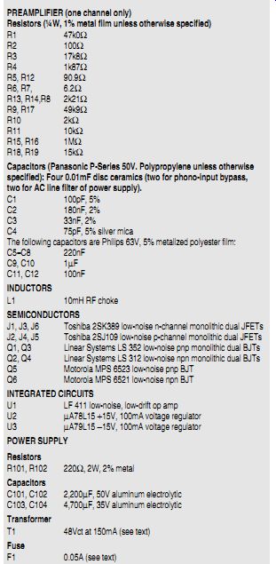
TABLE 1: PARTS LIST
PREAMPLIFIER (one channel only)
Resistors (¼W, 1% metal film unless otherwise specified) R1 47k0 ? R2 100 ? R3 17k8 ? R4 1k87 ? R5, R12 90.9 ? R6, R7, 6.2 ? R13, R14,R8 2k21 ? R9, R17 49k9 ? R10 2k ? R11 10k ? R15, R16 1M ? R18, R19 15k ? Capacitors (Panasonic P-Series 50V. Polypropylene unless otherwise specified): Four 0.01mF disc ceramics (two for phono-input bypass, two for AC line filter of power supply). C1 100pF, 5% C2 180nF, 2% C3 33nF, 2% C4 75pF, 5% silver mica The following capacitors are Philips 63V, 5% metalized polyester film:
C5-C8 220nF C9, C10 1µF C11, C12 100nF
INDUCTORS
L1 10mH RF choke
SEMICONDUCTORS
J1, J3, J6 Toshiba 2SK389 low-noise n-channel monolithic dual JFETs J2, J4, J5 Toshiba 2SJ109 low-noise p-channel monolithic dual JFETs Q1, Q3 Linear Systems LS 352 low-noise pnp monolithic dual BJTs Q2, Q4 Linear Systems LS 312 low-noise npn monolithic dual BJTs Q5 Motorola MPS 6523 low-noise pnp BJT Q6 Motorola MPS 6521 low-noise npn
BJT INTEGRATED CIRCUITS
U1 LF 411 low-noise, low-drift op amp U2 µA78L15 +15V, 100mA voltage regulator U3 µA79L15 -15V, 100mA voltage regulator
POWER SUPPLY
Resistors
R101, R102 220 ohm, 2W, 2% metal
Capacitors
C101, C102 2,200µF, 50V aluminum electrolytic C103, C104 4,700µF, 35V aluminum electrolytic Transformer T1 48Vct at 150mA (see text) Fuse F1 0.05A (see text)
-----------------------
Unfortunately, it was necessary to take what was available, and the n-channel and p-channel devices that I used are from different IDSS groups. I was able to find a sufficient number of complementary devices, nonetheless, through the use of a curve tracer. If possible, choose all "V" or all "BL." I do not recommend transistors from the "GR" group because of the possibility that some units have values of IDSS that are too low for this application.
You should certainly avoid getting one type from the "GR" and the other from the "V" group, since there is no IDSS overlap between the two. In quantities of 100 each, the prices drop to less than $1 per transistor. I am not at all sure that there are good substitution alternatives to these JFETs. Perhaps audioXpress will make some of these devices available if there is sufficient interest.
FEEDBACK-LOOP GAIN AND FREQUENCY RESPONSE
Notice that the output of the first-stage cascode is fed back to the input. No second or third stage is enclosed in the feed back loop. Also note that the feedback network is not frequency independent. A 180nF capacitor, C2, is added. At low frequency, this capacitor is effectively an open circuit, and the gain is As frequency increases, the capacitive reactance XC2 will decrease until it equals R3. This defines the 50Hz breakpoint of the RIAA curve. This breakpoint is a zero in the feedback factor because the effect of decreasing capacitive reactance shunting R3 is to increase the amount of feed back. As frequency increases still further, it finally reaches a point where an additional decrease in the capacitive reactance causes very little change in the feedback factor.
When the feedback factor is within 3dB of its ultimate and maximum possible value, the second breakpoint is reached.
This is a function of all three resistors and the capacitor, and occurs at 500Hz with the component values used. [21] You will recognize this as the 500Hz zero of the RIAA curve. It is, of course, realized as a pole in the feedback factor, since it represents the point at which the rising feedback caused by the feedback zero at 50Hz is cancelled.
In the absence of other higher poles and/or zeroes, the closed-loop response above 500Hz would be flat. This approach, then, avoids the unintended high-frequency zero of the noninverting single-stage RIAA amplifier that was mentioned at the outset.
An important design consideration is the absolute value of resistor R2. After it is set, the values of R3, R4, and C2 are set based on the desired closed-loop gain, the pole and zero frequencies, and the value of R2. Like R1, R2 can be a major contributor to circuit noise. Therefore, from a noise reduction perspective, it should be as small as possible.
Unfortunately, you are faced with yet another trade-off, since, ideally, the input resistance of the feedback network would be infinite. However, the lower the value of R2, the lower this input resistance will be, since R3 and R4 must be scaled accordingly. Power amplifiers have no problem driving low-impedance feedback net works, but many, if not most, preamps would.
OPEN-LOOP GAIN
Open-loop gain can also suffer if the feed back network loads the output. Low open loop gain a or low-feedback fraction ß can lead to deviations from the predicted value for closed-loop gain if, as a result, the closed-loop gain formula Afb = a/(1 + ßa) =1/ß becomes a poor approximation. ß = 0 for the no-feedback case, so that Afb = a.
Open-loop gain is usually quite vari able even among apparently identical amplifiers. As frequency decreases in the first stage, closed-loop gain rises, reflecting the decreasing value of ß necessary if the rising low-frequency response dictated by the RIAA curve is to be realized.
Feedback, which is the difference between the open- and closed-loop gains, is being squeezed. This, combined with the relatively low open-loop gain, means the assumption that ßa >> 1 (which is implicit in the approximate closed-loop-gain equation) must fail.
Precise RIAA tracking at low frequency is predicated upon Afb = ß-1(f). Since there was almost no error, even at 20Hz, the open-loop gain must still be adequate de spite the potential problems just discussed. There is absolutely no reason you could not use the component values given in AN 346, and doing so ameliorates the potential problem discussed in this paragraph. Since performances of two units were identical and precise, I decided to use the 100 ohmue for R2, and I proceeded from there.
While I don't intend to repeat the applications note, I do wish to present the formulas for the component values. This will allow you to customize the design, should you desire that. The technique in AN 346 is to set R2 based on the aforementioned trade-offs, choose a 1kHz first-stage gain in the range 10 = Afb = 30 (20 - 30dB), and then, based on these two factors, calculate component values starting with R3 = 8.058R2 × Afb.
From there, C2 = 0.00318/R3, and R4 = R3/9 - R2.
The formula derivations, found on the last page of reference 21, follow directly from the transfer function. There is al most always more flexibility in choosing resistor values than capacitor values, so the closest commercial 1% capacitor value may differ enough that it is necessary to recalculate R3 according to R3 = 0.00318/C2.
The applications note then calls for a recalculation of R2. I doubt that is necessary, however, because R2 does not affect the 50Hz RIAA breakpoint at all, and affects the 500Hz zero only slightly. It does have a major effect on the 1kHz gain, but this is not standardized, which is the reason a range is specified in the first place.
PASSIVE EQUALIZATION
There is, of course, another pole you must establish to conform completely to the RIAA curve. It is provided passively by the low-pass filter formed by R8-C3. Actually, the precise calculation of this pole frequency requires the Thévenin-equivalent resistance seen by C3. C3 sees R8||R9 rather than simply R8, so the technique used in AN 346 is first to choose a 1% capacitor value in the range of 10-50nF, then to compute an Rp = 75µs/C3 = 2k273 ohm.
The 75µs in the equation is simply the RC time constant corresponding to a pole at 2.122kHz. Since R8 and R9 are in parallel, choose a slightly larger 1% resistor value for R8. I chose the value of 2k37 ?.
Finally, compute R9 so that R8||R9 = Rp.
This can be done using R9 = 1/(1/Rp - (46dB) 198 R2 R4 R3
1 R2 R4 R3 R2
Av =
+
+ =
+ +
= .
----------------
EVALUATION FROM A FRIEND OF THE AUTHOR:
I got your preamp hooked up this evening into the Tape-2 input. It sounds great-very quiet and no hum at listening levels. The gain is definitely less than my PS Audio phono stage: I'm running the volume control at the 11:00 position, whereas it's normally at 8:00 for phono listening. I tried to match listening levels between your phono stage and my normal phono setup for a fair A/B comparison. Using Paul Simon's Graceland album, I noticed a wider and more three-dimensional soundstage, which seemed to be placed a bit lower. I don't recall any significant differences in musical detail, and it was definitely a clear, transparent sound.
-Mitch
---------------------------
1/R8) = 55k536 ohm. The nearest 1% value is 54k9 ohm.
Now I must 'fess up. Resistor R9 was required in AN 346 because the output of the first-stage op amp was capacitively coupled to the input of the second-stage amplifier, which was an LM833 bipolar op amp. Without R9, there is no input bias current path for the LM833. There is no such requirement in this design because the first stage is directly coupled to the second stage.
I left R9 in nonetheless, because I desired a stage that could serve purely as a phono section driving a separate preamplifier line stage through a 50k potentiometer if I should decide to incorporate the section into such a preamplifier in the future. I subsequently realized that if I were to do this, I would still need a buffer.
At this point, I would keep the current topology, but make the second stage a gain-of-ten (20dB) stage and reduce the 1kHz reference gain of the first stage accordingly. This, of course, would require recalculating the feedback-network component values. Lowering first-stage closed-loop gain is another way of easing any problem of low open-loop gain in that stage.
Omitting R9 seemed to make the frequency response-and consequently RIAA tracking-more sensitive to component-value variations. If you nevertheless decide to eliminate R9 altogether, PSpice shows that R8 = 2k15 ohm gives the proper attenuation at high frequency. It also, however, shows that R3 should be simultaneously reduced to 16k9 ohm; otherwise the boost at low frequency is excessive.
Since it is cheaper and easier to use a number of 1% resistors than 1% capacitors, I suggest that you vary R3 if low-frequency response needs trimming.
Eliminating R9 also ameliorates the low-frequency, open-loop gain degradation by increasing the impedance magnitude that the first-stage output must drive.
If you need lower output impedance for either the first or the second stage, you could easily add a follower/buffer. Of course, the whole idea was to keep it simple, and that would be a step in the wrong direction.
The early PSpice versions of the circuit used followers at the output of both stages. I eliminated these when PSpice indicated-and breadboarding confirmed- that the buffers were not essential.
You should note that R9 = 2k21 ohm, which is less than the calculated value of 2k37 ohm. This difference comes about because the output resistance of the first stage is not 0 ohm, as it very nearly is for the op amp-based design of AN 346. The output resistance of the first stage must be folded into the R9 value, or the pole frequency will be lower than anticipated.
Despite the shortcoming of my discrete one-stage op amp in the area of output impedance, I was able to achieve almost perfect high-frequency tracking of the RIAA curve, with the response dead on at most frequencies. The maximum errors measured were 0.1dB more attenuation at 20Hz and 0.1dB less attenuation at 20kHz than would be ideal. I have already alluded to the reason for the error seen at 20kHz.
The best feature is the reproducibility of the tracking. Both channels that I constructed tracked identically, and their gains at the 1kHz reference frequency were the same as the standard 1% capacitors and 1% metal-film resistors used at the breadboard stage. In one channel, I had no 1%, 33nF capacitor, so I hand-selected a 10% unit whose measured value was within the 1% tolerance band.
Since Digi-Key is a convenient source of parts for hobbyists using 2%-tolerance, 50V polypropylene capacitors, I ultimately used Digi-Key components in the prototype, and it is those capacitors for which the PC-board pattern is sized. Again, claims are made for sonic effects due to capacitor dielectric material, but I am skeptical of the existence of such effects.
Even so, polypropylene capacitors are objectively superior to most others, and they were the only precision capacitors available from this source.
Both channels of the prototype still track the RIAA curve with 0.1dB accuracy, but they do differ from one another by as much as 0.2dB, probably because of the relaxed tolerance on the capacitors.
Since there is a price break for quantity purchases, you could order them in lots of ten, using a capacitor meter to find units that fall within 1% of the design value if slight tracking deviation were a concern.
SECOND STAGE
It is possible to realize the entire 38dB of gain in the input stage, although distortion would be greater. To do so, it would almost certainly be necessary to increase the output-node impedance magnitude by increasing R2 and scaling the other equalization-network values accordingly.
In that case, or if you incorporated this phono section into a control preamp with a volume control of 50k ohm as previously discussed, the pot could then replace R9, and you could omit the second stage.
The increased distortion would probably be acceptable, but I did not like the idea of an unbuffered R8-C3 filter output driving an unknown downstream device.
Therefore, I faithfully followed the scheme of AN 346 with a second folded cascode single-stage op amp realized in discrete form. In fact, the second stage is identical to the first except for the feed back network.
All the equalization is taken care of in the first stage and the interstage low-pass filter. However, an additional flat gain of 10 to 20dB is needed to bring the 1kHz gain to a level where the output is in line with that from a tuner or CD player. The gain used here differs slightly from that of the AN 346, which is a result of trimming the second-stage gain by ear.
With an LP as the source, I simultaneously fed the same cartridge channel into the phono input of a Dynaco PAT 5 pre amp and my preamp. The output of my preamp was fed into the tuner input on the same PAT 5. I varied the gain of the second stage until the two signal paths produced the same speaker volume.
Therefore, I can say with certainty that the output level from this phono preamp is in line with at least one commercial preamp.
There is no output level adjustment, but this should not be a problem. The overall gain is within the range normally chosen for interfacing a moving-magnet phono cartridge with a preamplifier line stage. You can increase (or decrease) the value of R11 if you desire more (or less) gain.
Output Impedance
The magnitude of the output impedance at the drains of J5B/J6B is around 60 ohm.
This reflects the high open-loop impedance at this node that cannot be lowered below this value despite the large amount of negative feedback to be found in a gain of-6 configuration. Thus, if the preamp must deliver a lot of current, output volt age will fall rapidly. Still, this is not excessive output impedance for most circuits that would accept this output.
An advantage of the folded-cascode op amp is that load capacitance does not contribute to instability; rather, it enhances stability by lowering the dominant pole frequency. [22] I added capacitor C4 for stability of the second stage, since a high frequency oscillation existed under no load output conditions. I did so even though the oscillation, as expected, disappeared with the output connected to a preamplifier.
It is poor practice to offer a design that has even a remote chance of oscillating.
As was discussed elsewhere in Audio Electronics, [23] an excellent method of compensation, if it works, is to roll off the closed-loop response with a feedback zero such as that produced by the addition of C4. As it turns out in this simple design, pole spacing permits successful use of such a scheme. PSpice did not predict this oscillation, which illustrates that the CAD tools are useful, but have their limitations.
I am convinced that running the output into one additional gain-of-10 cascode stage that's otherwise identical to the second stage of this preamp will yield a perfectly acceptable signal that could directly drive a power amplifier. In other words, the additional stage would serve as the line-amplifier stage, and the control pre amplifier could be omitted if this were a phono-only system. For this, a 50k ohm dual potentiometer should be inserted between the second stage of this circuit and the new line-amp stage to serve as a volume control. You could build a complete control preamp around this topology if you so desired.
Cont: A PHONO PRE-PREAMPLIFIER FOR THE CD ERA, PT. 2
---------------------
REFERENCES
1. Manny Horowitz, How to Build Solid-State Audio Circuits, Tab Books/No. 606, 1972, p. 250.
2. Reg Williamson, "Understanding the RIAA Curve," TAA 2/90, p. 20.
3. Kerry Lacanette, Linear Applications Handbook, National Semiconductor Corporation, 1994, pp. 822-30.
4. David Johns and Ken Martin, Analog Integrated Circuit Design, John Wiley & Sons, Inc., 1997, pp. 266-73.
5. Nelson Pass, "Cascode Amp Design," Audio Magazine, March 1978, pp. 52-59.
6. Norman E. Thagard, "Build a Mono, 100-Watt Class A Amp, Parts 1, 2, and 3," Audio Magazine, January, February, and March, 1995.
7. Norman Thagard and Nelson Pass, "Build the A75 Power Amplifier, Parts 1 and 2," TAA, 4/92 and 1/93.
8. Paul Horowitz and Winfield Hill, The Art of Electronics, Cambridge University Press, 1989, pp. 441-42.
9. Sergio Franco, Design with Operational Amplifiers and Analog Integrated Circuits, Second Edition, Mc Graw-Hill, 1998, pp. 327-8.
10. Erno Borbely, "JFETS: The New Frontier," AE 5/99, p. 30.
11. Horowitz and Hill, op. cit., p. 444.
12. Erno Borbely, "A Moving Coil Preamp," TAA 4/86, p. 12.
13. Horowitz and Hill, op. cit., pp. 445-47.
14. ibid., p. 1006.
15. ibid., p. 869.
16. Erno Borbely, op. cit., pp. 27, 30.
17. Brian Clark, "DC Servo Loop Design for Audio Amplifiers," TAA 3/82, pp. 14-23.
18. Johns and Martin, op. cit., pp. 269-70.
19. Douglas Self, "Distortion in Audio Power Amps, Part 1," AE 2/99, pp. 19-20.
20. Horowitz and Hill, op. cit., pp. 90-91.
21. Lacanette, op. cit., p. 830.
22. Johns and Martin, op. cit., p. 268.
23. Norman E. Thagard, "A Case Study in Audio Amplifier Design, Part 1," AE 5/99, pp. 16-18.
Also see:
A PHONO PRE-PREAMPLIFIER FOR THE CD ERA, PT. 2
Link |