This author makes good use of 2E24 tubes to produce a single-ended amp with plenty of power.
By Don Kang
Since the return of the vacuum tube amplifier to the high-end audio scene, I have wanted to build a WE300B SE amp. However, the price tag of the WE300B turned me off. When I found a dozen 2E24 tubes at a local ham swap for $1 each, my desire to build the SE amp re-ignited.
The 2E24 is a filament version of the popular 6146, but one size smaller.
According to the GE data book, the 2E24, as a beam tube, delivers 3.9W of power. By doubling two, the output power becomes 7.8W, which is about at the WE300B power level.
IDEAL AMPLIFIER
My ideal amplifier has the following requirements:
1. A directly heated triode for the final power amplifier tube
2. Single-ended configuration
3. No capacitors in the grid signal paths
4. No overall (global) negative feedback
5. Only one stage triode voltage amplifier
This amplifier consists of two tubes:
one resistor and one transformer (Fig. 1.).
---- ABOUT THE AUTHOR
Don Kang is an electronic engineer specializing in silicon chip making. He enjoys various DIY projects.
Currently he is busy with submarine torpedo power systems for USN. He has a Ph.D from the Ohio State University and is a lifetime member of the IEEE.
2E24 POWER AMPLIFIER STAGE
Before I started this amplifier design, I wanted to know how other people were using the 2E24 tube for audio applications. Based on my limited search, I found nothing. I used a Tektronix 577 curve tracer to obtain the plate characteristics of the 2E24 in triode mode connecting the screen grid to the plate. For a power tube requiring a higher grid voltage, you need an external voltage source.
Because of the anticipated paralleling operation, I manually plotted all 12 tube plate V/I curves on a 0.1” grid paper (Tops #35101). There was some spread in the V/I curves, but I found no problem in pairing them up because I had so many.
I checked the screen grid current with a low resistance resistor, which is placed in series with the screen grid. The power loss was acceptable.
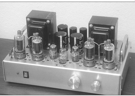
PHOTO 1: The completed unit.
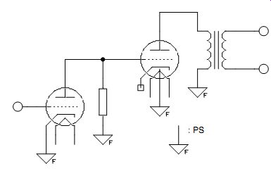
FIGURE 1: My ideal amp.
You can graphically estimate the power output on the V/I curve plot by selecting a load line and control grid swing along the load line. The 2E24 has maximum plate power dissipation of 10W and maximum plate voltage of 250V. First, I entered these two quantities on the V/I curve plot (Fig. 2). The point "S" satisfies both requirements. I drew a tangential line at "S." This is a load line and "S" is an operating point.
For a normal operation, the control grid swings to the positive direction from -22V to 0V and swings to the negative direction with the same amount from -22V to -44V.
The grid swing on the load line forms a side of the shaded triangle (abc). The area of this triangle (abc) represents the power output. The load line meets X-axis at 510V and Y-axis at 78mA. The load impedance is 510V/78mA = 6.53k-ohm.
At the operating point "S," Vp = 250V, Ip = 40mA, and Vg = -22V. The vertical distance <ac> represents current swing ?i, and the horizontal distance <cb> rep resents voltage swing ?v.
The formula for the power output Pout is:
Pout =delta_i ×delta_v/8 = (390-108) V × (61-18)mA/8 = 1.51W
This is too low. Readjustment of load line did not increase P_out much. To make this triangle much larger, it should expand in all directions. Since I do not have any other application for 2E24s, I decided to explore the 2E24 further.
CLASS A2 OPERATION
For a normal Class A1 amplifier, the control grid stays in the negative potential at all times. There are some transmitting tubes operating in the positive potential with respect to the cathode.
This kind of operation is classified as Class A2. In order to find the possibility of A2 operation, I plotted the plate V/I curve with the control grid voltage of +5V and +10V.
Knowing the Pd max. of 10W, I was very careful not to exceed this limit. I lowered the plate voltage of the 577 curve tracer whenever possible during the Class A2 investigation. Fatal mis take! I lost two 2E24s. The control grid was shorted to the filament. An autopsy revealed that a molten metal ball was touching the filament.
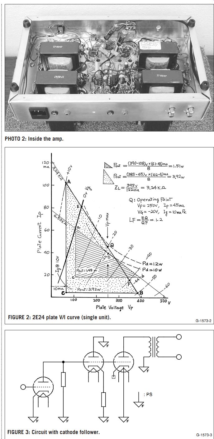
PHOTO 2: Inside the amp.
FIGURE 2: 2E24 plate V/I curve (single unit).
FIGURE 3: Circuit with cathode follower.
When the control grid is in the positive potential, the grid and the plate are competing to attract electrons. As the plate voltage goes low, the grid absorbs more electrons. For a given positive grid voltage, as the plate voltage decreases, the electron current to the grid increases very rapidly. The energy dumped by the electrons melted the grid wire. The molten liquid of grid wire formed a round ball due to the surface tension. This liquid ball was big enough to bridge the distance between the grid and filament.
To get more power output, the plate dissipation is relaxed to 12W and Class A2 operation is permitted with the following conditions. With non-continuous base, the control grid can take as high as +10V and 10mA. In order to en sure the 10mA limits, the plate voltage should be kept no lower than 65V at all times.
With this new guideline, you obtain a larger dotted triangle (ABC) in Fig. 2.
The point "A" is automatically set by +10V of control grid and 65V minimum of plate voltage. The highest impedance load line is from "A" to the Pd = 12W line. Unlike the shaded triangle (abc), the operating point Q is not on the 12W line but on the load line at 250V.
At this operating point, Vp = 250V, Ip = 45mA, and Vg =-20V. The grid swings from -20V to +10V to the positive direction and from -20V to -50V to the negative direction. The total swing is 60V.
The load impedance is 395V/122mA =3.24k ohm. The position "A" is 65V, 102mA, and the position "B" is 385V, 4mA.
Pout = (385-65) V × (102-4) mA/8 = 3.92W
When two 2E24s are paralleled, the load impedance becomes 1.62 k-ohm and the output power doubles to 7.84W.
LINEARITY FACTOR
The grid voltage line intersects the load line on the plate V/I curve. The distance between the intersecting points is not equal. Near the operating point, the changes are uniform and the distance becomes progressively smaller toward the X-axis.
Taking the well-behaved middle part near the operating point, the "Linearity Factor" (LF) will be introduced. In this case, the region to be used is from Vg = 0 to Vg =-40; that is a 20V range on both sides of the operating point Q.
LF = distance <EQ>/distance <QF>= 1.2
This means the positive half of the signal is amplified 20% more than the negative half. This unbalance can be cancelled out if the voltage amplifier does the opposite. As a matter of fact, the following voltage amplifier will do just that.
Summary of the 2E24
Power Amp Design:
Operating Point Q: Vp = 250V, Ip =
45mA ×2, Vg =-20V Vg swing: +10V to -50V, total 60V (peak to-peak) Ig: 10mA × 2 at the positive peak Pout = 3.92 × 2 = 7.84W LF = 1.2 ( ×2 means two tubes)
VOLTAGE AMPLIFIER
A nominal input signal of 0.5-1.0V RMS should produce a 60V PP output. Taking the midpoint figure of 0.75V, the gain required is 60V/0.75V × 2 × 1.4 = 60V/2.1V = 28. Many small signal triodes are capable of giving a gain of 28, but none of them can supply 20mA of current at the positive peak. They are operating with a few milliamperes or less of plate current.
A very low output impedance device with 20mA of driving capability should be inserted between the voltage amp and the 2E24. A cathode follower is an impedance transformer ideally suited for this application. Because of the finite value of the output impedance, though it is very low, there is a voltage drop equal to the product of output impedance and the driving current. The voltage drop I can tolerate is 0.5V. At 20mA, the maximum impedance is 0.5V/20mA = 25 ohm.
The output impedance of a cathode follower is given by the formula
Zout = rp / (µ+1).
For a large µ, it becomes
Zout = rp/µ= 1/gm= 25 ohm gm= 40,000µS
... where rp is plate resistance, µ is voltage gain, and gm is transconductance. Any triode tube with transconductance of 40,000µS or more can satisfy the driving condition.
Going through the tube data book for higher gm, I chose the 5842 and 6KN8 (or 4KN8). When the two sections of the 4KN8 triode are paralleled, the gm value doubles to 32,000µS, which is higher than the 24,000µS of 5842. The gm value is not quite 40,000. The voltage drop is 20mA × 1/32,000µS = 20mA × 31 ohm= 620mV, which is acceptable.
The circuit with cathode follower is shown in Fig. 3. The 4KN8 has a µ of 45, which is also adequate for the voltage amplifier. Figure 4 is a plate V/I curve for the 4KN8. As discussed at the 2E24 design, the nonlinearity introduced by the 2E24 can be cancelled out at least near the operating point because the polarity of the signal is re versed from the voltage amp to the 2E24 power amp. The cathode follower does not reverse the polarity, and the linearity factor is considered very close to unity. Thus, all the compensation is taking place at the voltage amplifier stage. If you have a two-stage amplifier, you must come up with a combined linearity factor to match that of the power amplifier.
After a few trial load lines, I selected a 46k-ohm load with 170V plate voltage. This selection met LF of 1.2. The operating point was Vg =-1.5V, Vp = 70V and Ip = 2.2mA. I chose the 1.5V because of the possibility of using a battery.
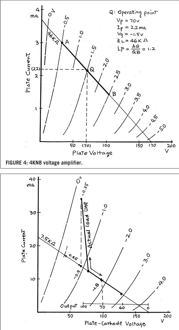
FIGURE 4: 4KN8 voltage amplifier.
FIGURE 5: 4KN8 cathode follower (both sections).
CATHODE FOLLOWER
Unlike the voltage amplifier, the cathode follower handles a peak current of 20mA on top of its normal current. The plate V/I curve in Fig. 5 shows the 4KN8 cathode follower operating in higher current with both triodes in parallel. I chose the cathode resistor of 7.5 k-ohm and 170V of plate voltage, which gave a good compromise between power dissipation and high current operation.
A cathode follower is an amplifier with the load connected at the wrong side of the power supply. The V/I curve still works with this connection. The amplified signal appears at the cathode side and becomes a part of the input in the reverse direction, thus producing 100% negative feedback. All the gain is reduced to one.
At the no signal condition, the cathode follower grid is at 70V and the output voltage is 71.8V. When the output voltage hits 91.8V (Vg = 0), the 2E24 grid starts to draw current. At its peak the current reaches 20mA. In order to support an additional 20mA, the cathode follower grid voltage takes a new value of -0.25V from -0.9V.
The net change is 0.65V. This is a reasonable agreement with the figure obtained with the gm value alone. This amplifier is no longer my ideal amplifier because of the cathode follower insertion.
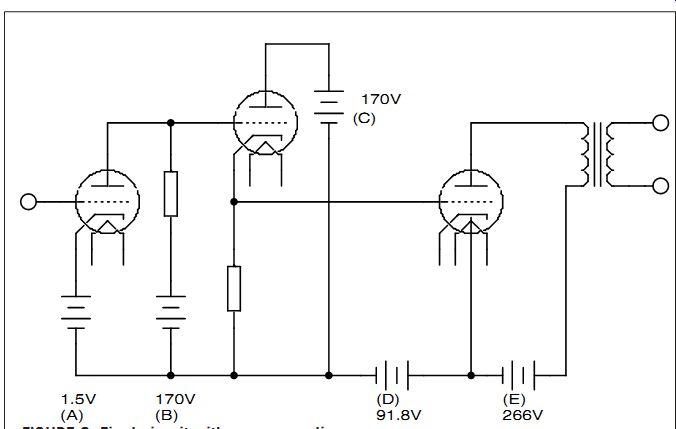
FIGURE 6: Final circuit with power supplies.
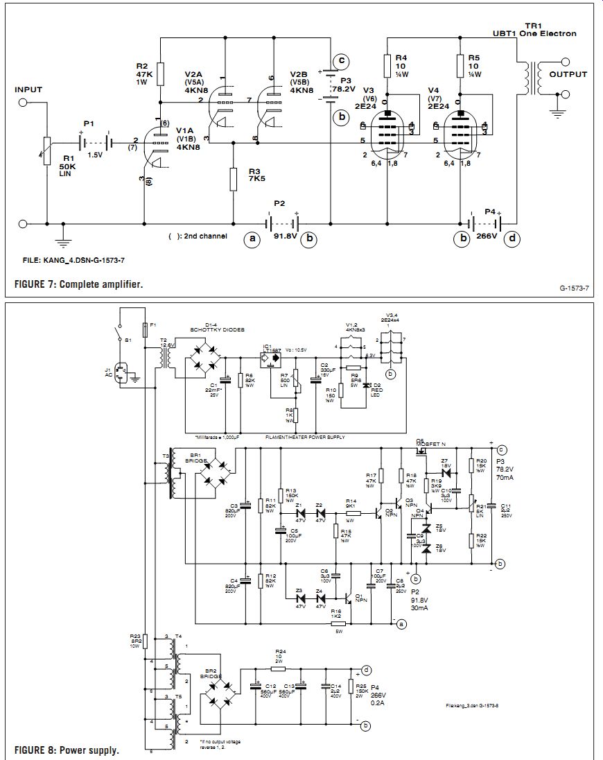
FIGURE 7: Complete amplifier.
FIGURE 8: Power supply.
POWER SUPPLY
All the power supplies are added in Fig. 6. If the filament/heater supply is included, a total of six power supplies are needed. Using all independent supplies is ideal.
This amplifier has three signal levels. The lowest level is the input level.
The next level is the signal at the output of the voltage amplifier. The same signal is at the input of the 2E24 power amp. The highest signal level is at the output of the 2E24.
The power supply 170V (B) and 170V (C) could be combined. This is okay be cause the voltage is not only the same but also associated with the same signal level. The power supply 91.8V (D) also handles the same signal. The complete amplifier circuit with rearranged power supply is shown in Fig. 7.
Because of the DC nature of this amplifier, any drift in the power supply voltages will alter the operating conditions. The impedance "Z" is defined as Z =?V/?I. If the output voltage is stabilized while the current is changing, delta_V = 0 and delta_I ? 0. Thus Z = 0. It is an ideal power supply. The output impedance of a voltage-regulated power supply is much lower than an unregulated one.
Since the P1 (1.5V) supply does not carry any current and handles the lowest signal, a battery is an excellent choice. This independent source produces a pure DC power. The life is 2-3 years with an AAA alkaline battery, which is directly connected to the grid of the voltage amplifier. Using a smaller watch type battery with a holder may be a better way. Today, shelf life of a 5-10 year battery is available. This connection makes the potential of the voltage amplifier cathode at ground level.
The P2 (91.8V) is regulated with a zener diode circuit known as "amplified zener." The P3 (78.2V) requires better regulation for the 20mA peak current. One transistor error amplifier and one power MOSFET pass element takes care of the regulation. A higher gain circuit can give a lower output impedance, but it may become unstable as the circuit becomes warmer. The P4 (266V) is for the 2E24 plate supply. Because it handles a high-level signal and it is independent, close regulation is not required.
I used three isolation transformer N 68Xs (50VA, 115/230) for all the plate supplies. The heater/filament supply is a regulated 10.5V DC voltage source...
TABLE 1
P1 (1.5V) P2 (91.8V) P3 (68.2V)
100Hz 0.73 2.36 0.47
1KHz 0.27 0.54 0.36
10KHz 0.12 0.13 0.21 ohm
...from a 12.6V filament transformer. Because of their small size, I mounted all four transformers at the bottom of the chassis.
A delay circuit is incorporated in the P3 supply to keep the 2E24 off for about 50 seconds. The C5 and R13 in the P3 diagram make up the delay timing. I placed an 8.2?/10W power resistor at the V4 transformer primary circuit to get the right voltage to the plate. I did not like the use of a power resistor to reduce the voltage here, but there was no simpler way. Since it was working, I decided to keep the resistor. The complete power supply circuit is shown in Fig. 8.
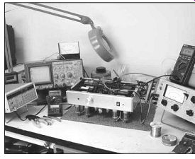
PHOTO 3: On the test bench.
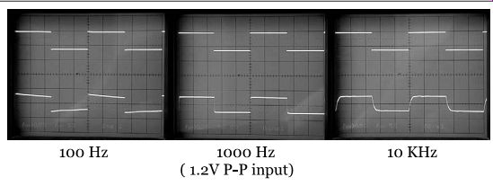
FIGURE 9: Rectangular wave input response.
I have read many tube amplifier articles describing changes in sound quality when power supply capacitors, chokes, rectifiers, and even the AC power cord, are changed. To me, this is similar to a situation in which you have built a fancy soundproof room, yet you are hearing sound leaking in from the next room and even from the rooms beyond.
The audio frequency spectrum is very wide. It ranges from near DC to 100kHz where the signal can readily escape to the space. The impedance of re active components is directly related to the frequency. Many aluminum electrolytic capacitors that work well at low frequency start to lose their function as capacitors when the frequency approaches 10kHz. It becomes a resistor, and beyond that it acts more like an inductor. Some non-electrolytic capacitors exhibit a sharp peak or dip at the high end of the spectrum.
All the capacitors have a resistor element called "Equivalent Series Resistance" (ESR). Most of the aluminum electrolytic capacitors have high ESR.
The capacitors in the high voltage sup ply are primarily for AC line hum reductions. These capacitors are also providing a return path for the signals.
When the power supply is connected in series with the transformer, the power supply becomes a part of the load.
If the impedance of the power supply is not low, a significant amount of signal voltage is induced at the power sup ply terminals, and this voltage will be distributed back to the voltage amplifier stages through the RC de-coupling circuit, which is frequency dependent and not perfect. Some attenuated signal will arrive at the input of voltage amplifier as a feedback signal. This is the case if only one plate voltage source is used.
When any one of the power supply components is replaced, impedance will be modified. You are certainly changing your amplifier "equalizer" settings in a very complex way. The power supply impedance should be low enough not to influence sound quality.
A dedicated plate voltage supply or separating DC and signal path of the final amplifier will cure the problem.
Another power-supply-related problem is RF noise when you use silicon rectifiers. A silicon PN junction generates RF noise pulse from its reverse recovery. If the power supply circuit provides a right tank circuit for the RF noise, it is amplified and escapes as a radio wave. The entire amplifier be comes polluted. Some ride with signal; some are rectified and modify bias conditions. Use of fast recovery rectifiers, different circuit components, and physical layout can minimize this problem.
CONSTRUCTION AND TUNE-UP
The performance of this amplifier is directly related to the quality of the output transformer. I used a pair of One Electron UBT-1s from Antique Electronic Supply, Tempe, Ariz.
Other than a pair of output transformers, there are no critical parts. You may use what you already have, but do not forget that the capacitors in the power supply circuits should provide an easy path (low impedance) for the return signals.
Though I experienced no instability with this amplifier, it is always a good practice to make wirings short and se cure. Semiconductor parts are not as generous as vacuum tubes when it comes to the mistakes. Even when the power is off, some residual charge in the capacitor may destroy semiconductor parts.
Make sure the capacitors are fully discharged before you make any measurements or replace parts. For the bleeder resistor, I used higher resistance values for lower power losses.
You should test all four power supplies individually with a proper dummy load.
Because the design is based on the actual plate V/I curve, the operating conditions should be close to the de signed values. The main voltage to home-in is -20V at the 2E24 control grid. If any adjustment of the bias voltage is needed, tweak 46k-o load resistor or P3 voltage.
I temporarily placed a 10 ohm resistor at each 2E24 plate to check the matching status. Because the voltage drop is only about 0.5V, I did not bother to remove the resistors afterward.
PERFORMANCE AND MEASUREMENTS
The frequency response is flat from 20 to 50kHz/2dB at 1W. The rectangular wave input responses at three different frequencies are shown in Fig. 9. The total harmonic distortion is plotted in Fig. 10.
The linearity factor used at the amplifier design was 1.2. Further adjustment made no significant changes on the distortion figure. I took all the test measurements with a 4-ohm 10W power resistor as the load. I measured the output impedances of the P1, P2, and P3 with full power seen from the load and listed them in Table 1.
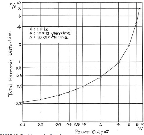
FIGURE 10: Total harmonic distortion.
HOW DOES THIS AMPLIFIER SOUND?
The sound is coming from a speaker. To evaluate an 8W amplifier, you should connect it to a relatively high efficiency speaker. My speaker system is a transmission line construction using Audax HM170Z0, HM170G0, and Raven R1 in a D'Appolito configuration. The sensitivity is about 91dB/W/m.
Some of us have misconceptions regarding the output transformer primary impedance. The specified impedance can be realized only when the right impedance load is connected at the secondary terminals. Any deviation will be reflected back to the primary side by the square of the transformer turns ratio.
Modern speaker systems contain many reactive components. Very often, the speaker itself has an impedance peak that is several times higher than the published value. If the speaker impedance seen from the amplifier is off from the designed value, expected performance may not be realized.
For the sound evaluation, I like to listen to the human voices that are directly recorded. We have a better appreciation of human voices than any other sound. This amplifier sounds very clean and clear. At a moderate power level it is very natural.
By today's standards, this amplifier is by no means a low distortion amplifier. At a normal listening level of a few watts, the total harmonic distortion is probably 100 times higher than today's high-end amplifiers. However, the distortion of this amplifier is as low as it can get without negative feedback.
WHAT I LEARNED
When paralleling the output tubes, a matched pair is mandatory. For lower distortion, matched linearity of the power tube and voltage amplifier tube is just as important. More emphasis should be placed on the combined linearity rather than the individual tube linearity. Many designers rely on the negative feedback for linearity improvement. However, the feedback should be the secondary means.
I placed a greater emphasis on the power supply impedances and the separation of power supplies. I believe that the low impedance and use of separate power supplies really helped to avoid high-frequency instabilities and cross couplings. This amplifier has no band width limiting components except the output transformers.
This project has motivated me to study a large number of plate V/I curves on many different tubes. I have ob served, within the same family, the DC parameter variation of as much as 50%.
Even supposedly identical twins in the same envelope exhibited unacceptable variations.
However, the AC parameter variations were far less than the DC counter parts. When directly replacing tube A with tube B of the same family, tube B may not operate under the same conditions. Thus tube B generates a different set of distortion patterns. The tube comparison by direct replacement can be very misleading.
I need to point out what the "matched pair" really means, and also the term "average" plate characteristics. The parameter variation of ±20% is very common. Without the knowledge of the actual plate V/I characteristics, it may be very difficult to optimize the amplifier performances. As with de signing a custom suit, you must know the body dimensions.
The Linearity Factor used is an indicator of second harmonic distortion.
Using a different LF value, you can control the second harmonics in the output. I choose to handle this topic separately as a sound-making tool for the SE amplifier. ?
-------------
ITEM VALUE/ DESCRIPTION PART NUMBER SOURCE
RESISTORS
R1 50k variable---linear R2 46k 1W R3 7.5k 2W R4, 5 10?¼W R6, 11, 12 82k ½W R7 500 ohm Variable--linear R8 1k ½W R9 5.6? 5W R10 150?½W R13 150k ½W R14 9.1k ¼W R15, 17, 18 47k ½W R16 1.2k 5W R19 3.9k ¼W
R20, 22 15k ½W R21 5k variable--linear R23 8.2 -ohm 10W R24 10 -ohm 2W R25 65k 2W CAPACITORS C1 22,000µF 25V electrolytic P-6461-ND Digi-Key C2 330µF 16V electrolytic P-10246-ND Digi-Key C3, 4 820µF 200V electrolytic P-6830-ND Digi-Key C5, C7 100µF 200V electrolytic P-7517-ND Digi-Key C6, 9, 10 3.3µF 100V electrolytic P-10767-ND Digi-Key C8, 11 2.2µF 250V polyester 23MA522 Mouser C12, 13 560µF 400V electrolytic P-10153-ND Digi-Key C14 2.2µF 400V polyester 146-400V 2.2K Mouser
SEMICONDUCTORS
BR1, 2 Bridge rectifier 800V/1A 2KBB80R-ND Digi-Key D1, 2, 3, 4 Schottky rectifier 60V/3A 31DQ06-ND Digi-Key IC1 Voltage regulator LT1587CT-ND Digi-Key Q1 NPN power transistor TIP41CTU-ND Digi-Key Q2, 3, 4 NPN high voltage transistor MPSA42-ND Digi-Key Q5 N-channel power MOSFET IRF630N-ND Digi-Key Z1, 2, 3, 4 Zener diode 47V 1N4756ADICT-ND Digi-Key Z5, 6, 7 Zener diode 8V 1N4756ADICT0ND Digi-Key LED 5mm red 606-FLV110 Mouser
OTHERS
F1 Slow blow 2A fuse P1 1.5V AAA alkaline battery MN2400 Duracell T1 One Electron Transformer UBT-1 Antique Electronic Supply T2 12.6V/3A Filament Transformer 553-F224X Mouser T3, 4, 5 115/230 Isolation Transformer 553-N68X Mouser (1,2: red, 3: blk, 4: yel/blk, 5: red/blk, 6: grn/blk, 7: wh-ground) V1, 2 4KN8 vacuum tube 4KN8 Antique Electronic Supply V3, 4 2E24 vacuum tube 2E24 Antique Electronic Supply
------------------
Also see: AMPLIFIER MUSICALITY