By Erno Borbely
This flexible phono preamp design benefits from the author's 40 years of experience in the business.
The EB-804/419 is a high quality, low-cost all-JFET DC-coupled MM/ MC phono preamp with on-board all-FET regulators. The combination of low input noise and high gain allows you to use it with practically all pickups on the market. The EB-804/419 uses a two-amplifier approach instead of the usual single amplifier. This allows you to optimize it for low noise, RIAA accuracy, high gain, and dynamic range.
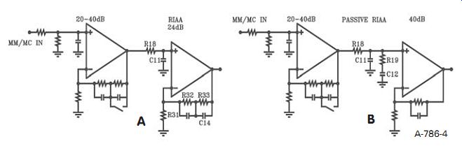
FIGURE 4: Block schematic for EB-804/419.
The block schematic is shown in Fig. 4.
You can use the two-amp configuration in three different ways to realize the RIAA function: all active, all passive, or hybrid, meaning combination of passive and active. Two of these are supported in the EB-804/419: the hybrid and the all passive.
In Fig. 4A the amp on the left is a high-gain amplifier with extremely low input noise and flat frequency response. You can use it with 20 or 40dB gain by changing the feedback resistor. The R18/C11 network between the two amplifiers provides the 75µs passive rolloff. The second amp provides a further amplification of 24dB at 1kHz and at the same time boosts the bass according to the RIAA characteristics actively through R33/R32/R31/C14.
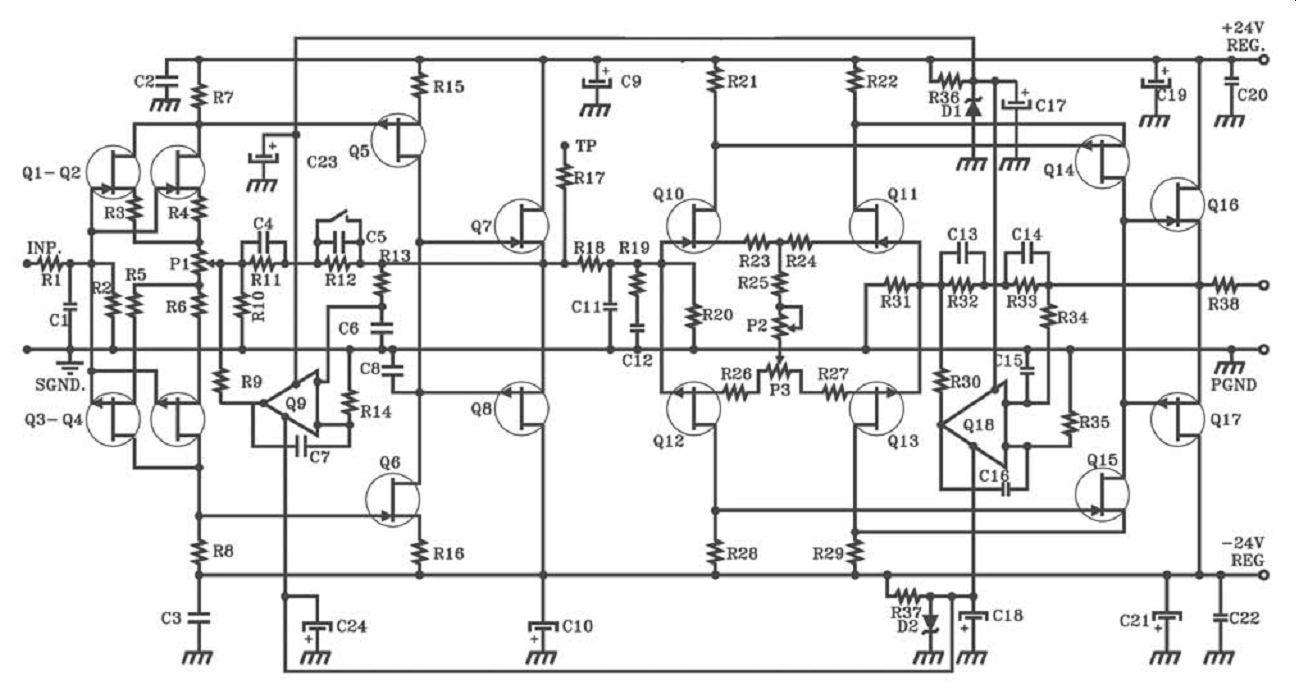
FIGURE 5: The EB-804/419 all-JFET MM/MC phono preamp.
For those of you who want to experiment with all-passive equalization I have included the components for Walt Jung's network N26,7 in Fig. 4B. Here both amplifiers provide flat frequency response and all RIAA equalization is done passively between the two amplifiers by R18/C11/R19/C12. MM gain is 44dB and MC gain is 64dB for the circuit in Fig. 4A. The gain in Fig. 4B depends on the all-passive equalization network discussed later. The Starter kit is supplied with components for the circuit in Fig. 4A. You can order the all-passive network separately from Borbely Audio.
Figure 5 shows the schematic of the EB-804/419. The input stage is essentially the same as the one in Fig. 3B, but I have added source resistors to each of the input JFETs in case these are needed for matching and/or adjusting the drain current. Because the DC gain of the circuit can be very high (MC application and/or all-passive equalization), I use a servo circuit instead of capacitive coupling to keep the offset close to 0V.
I calculated the equivalent noise resistance of the input stage using the drawing in Fig. 6. The JFETs are represented by the 55 __ equivalent noise resistors in series with the 10 ohm source resistors. These are connected to P1, which is a 10 __ trimpot. Finally, the center point of the trimpot goes to R10 = 6R8 feedback resistor.
Because the JFETs are connected in parallel AC-wise, the equivalent noise resistance can be calculated to 25.5 __. This will produce 92nV over the audio bandwidth. If you use this preamp with a 50 ohm MC pickup, you will have a total noise of v1282 + 922 = 157.6nV, which results in a signal-to-noise ratio of 70dB referred to 0.5mV.
The 50 ohm pickup itself contributes 128nV--i.e., if the amp were noise less, the signal-to-noise ratio would be 71.8dB re 0.5mV. This means that the amp contributes only 1.8dB to the noise. You could decrease this by reducing/eliminating some of the noise-producing resistors in the input circuits.
If you select the input JFETs very closely, you could eliminate the 10 ohm source resistors. The close matching could also eliminate the offset trimpot.
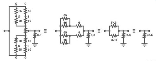
FIGURE 6: Calculating the equivalent noise resistance of the input stage.
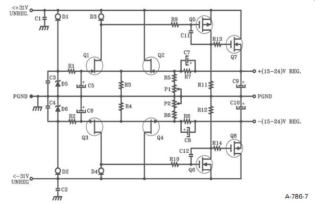
FIGURE 7: EB-704/418 all-FET regulators.
This would result in an equivalent noise resistance of 20.5 ohm with a signal-to noise ratio of 70.4dB, which means that the amp would contribute only about 0.4dB to the overall noise. For a 50 ohm MC pickup this is probably the best you can achieve; however, for lower impedance/lower output MC pickups you will need to reduce the amp noise even further. (Calculate the signal-to-noise ratio for an MC pickup with 20 ohm resistance!)
For MM the feedback resistor R10 is 75 ohm, and the equivalent noise resistance is 93 ohm. The equivalent short circuit input noise is 175nV. The total input noise with a 600 ohm MM pickup is v (445^2 + 175^2) = 478nV, and the signal to-noise ratio relative to 5mV is 80dB.
The second stage of the phono preamp uses the same topology as the Starter kit EB-604/4104. It provides the active bass boost of the RIAA characteristic through its feedback network. However, due to its high DC gain (in active eq. mode the DC gain is 44dB!) a servo has been added. The servo amps are sup plied with ±10V from shunt regulators.
The all-FET phono preamp is a very sensitive amplifier and is capable of picking up small signals not only through its inputs, but also through vibration. It is, therefore, very important to make the whole amp as "dead" as possible for vibration by using rubber stand-offs or mounting the whole board on a Teflon plate, 6-8mm thick. And a mumetal box will certainly put the icing on the cake.
TYPICAL SPECIFICATIONS
Gain: 1st stage: 20 or 40d
THD, 20dB gain, 3V/1kHz: 0.0033%
3V/10kHz: 0.005%
Gain: 2nd stage: 24dB THD, 3V/1kHz: 0.003%
3V/10kHz: 0.007%
Max. output voltage: approx. 9V RMS Risetime
(without RIAA network): 0.3/0.4µs
Freq. Response: RIAA ±0.2dB
Equivalent input noise: <100nV, 20Hz-30kHz
THE EB-704/418
ALL-FET ON-BOARD REGULATOR
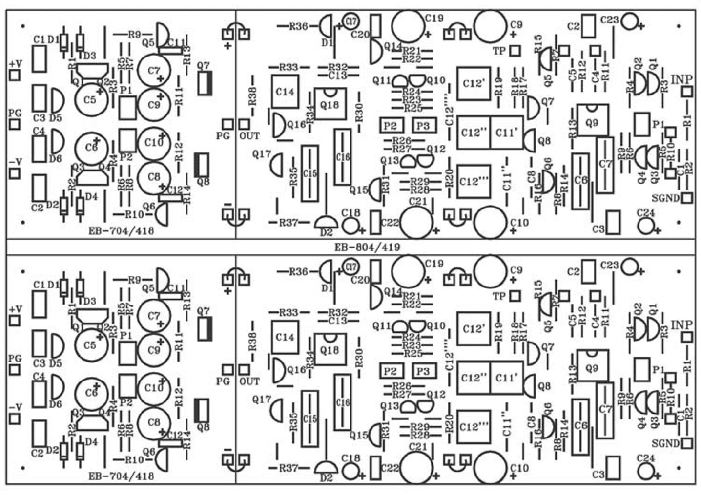
FIGURE 8: Stuffing guide for MM/MC phono preamp EB-804/419 with EB-704/418 regulator.
The schematic of the on-board EB 704/418 all-FET regulators is shown in Fig. 7. The topology is very similar to the EB-604/415 regulators used in the EB-604/410 line amp described in reference 4. However, I added Q7 and Q8 MOSFET source followers to be able to cope with the demand of the phono preamp (70mA). You can change output voltage between 15 and 25V with P1 and P2. If you use them with fixed 24V output, then you can short P1 and P2.
Make R5 = R6 = 3k32.
Minimum input/output voltage differential is 3V, but 4V is recommended.
Maximum unregulated input voltage is ±31V, and you must heatsink Q7/Q8.
The output noise of the regulators is <5µV across the audio bandwidth. Recommended power supply is the EB-604/265. The stuffing guide for the EB-804/419 phono preamp is shown in Fig. 8.
SETUP PROCEDURE
Start the assembly with the regulators, insert the solder pins and the jumpers, and then install the resistors, FETs, and finally the capacitors. Connect 332R/5W resistors between the +output and ground and the -output and ground of the regulators. Apply ±29V unregulated DC to the regulators. Check the output voltage across the load resistors; it should be 24V, ±5%.
Next, begin the second stage of the phono preamp (R20 and onwards) by installing all solder pins, jumpers, resistors, JFETs, and capacitors. Put in the supply jumpers between the regulators and the second stage and short the input of the second stage (jumper across R20). Do not install Q18 just yet. Connect the ±29V unregulated supply to the regulators. Measure the voltage drop across R22 (or R29) with a DVM and adjust it with P2 to 3V. Then check the offset voltage at the output and adjust it with P3 to 0V. Insert Q18 in the socket and recheck the offset; it should be less than a couple of mV after a few seconds.
Finally, assemble the input stage, except the RIAA components between the two amps and Q9. Disconnect the supply jumpers between the regulators and the second stage and connect the regulators to the input stage with short wires.
Short the +INP-pin of the input stage to SGND and check the voltage across R15 (or R16), which should be between 2.8V and 3.3V. Check the offset voltage of the input stage at the test-point TP and adjust it to zero with P1 (do this very carefully because the DC gain is very high). Install Q9 in the socket and recheck the offset, which should go down to a couple of mV in a few seconds.
Remove the jumper from R20, install the RIAA components, and connect the proper supply jumpers between the regulators and the second stage and between the second stage and the input stage. Leave the short at the +INP and switch on the supply voltage. Check the offset at the output, which, after a couple of minutes, should be a few mV. A certain short-term drift of the offset is normal-remember, you are dealing with a total DC-gain of 84dB! If you have audio measurement equipment, including an inverse RIAA circuit8 connect it to the input of the phono preamp and sweep the audio generator from 20Hz to 20kHz. Monitor the output of the phono preamp with an audio mV-meter. The output voltage should be constant with a maximum tolerance of ±0.2dB. If you have a scope, connect it to the output and make sure that the circuit does not overload during the measurement.
-------
RIAA EQUALIZATION
The RIAA characteristic is de fined by three time constants: T1 = 3180µs, T2 = 318µs, and T3 = 75µs, corresponding to the crossover frequencies of 50, 500, and 2122Hz. A fourth time constant of 7950µs has been added by the IEC as an amendment to the RIAA characteristic; however, it has never been officially standardized by the RIAA. This time constant means a 6dB roll off below 20Hz, and is meant to function as a rumble filter, reducing turntable/record related low frequency disturbances. This feature is not included in the phono preamp described here.
The RIAA characteristic is shown in Fig. A with the a-symptoms. It is specified in dB relative to 1kHz (0dB). It appears that the DC (or zero frequency) gain is 20dB (10×) higher than the gain at 1kHz. However, be cause of the interaction between the time constants, the actual DC gain is 9.898× the gain at 1kHz. This means that in an ideal RIAA preamp the 1kHz gain is always 0.101×DC gain (see reference 6: Walt Jung; Op Amp Applications, Chapter 6-1, Analog Devices, 2002, ISBN:0 916550-26-5), so specifying the gain at 1kHz also defines the gain for all other frequencies.
-----------------
The phono preamp is now ready to be connected to your system. Changing between MM and MC means replacing R10. For MM, R10 = 75R and for MC it is 6R8. For MM, R2 is 47k, and for MC you will need to connect the appropriate load resistor at the input.
You can solder this resistor either directly across the input terminals of the PCB or across the input connector on the back panel. A shunt capacitor (C1) might also be necessary; consult the datasheet of your pickup.
Acknowledgements
Many thanks to Walt Jung for letting me use his passive RIAA network in the phono preamp and for his valuable comments and suggestions regarding this article.
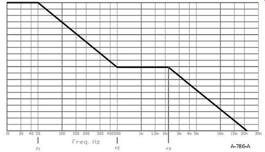
FIGURE A: The RIAA playback characteristic.
-------
DESIGN PROCEDURE
The design procedure for the hybrid circuit in Fig. 4A is relatively simple:
1.) 75µs passive network: choose an appropriate value for R18, which should be as low as possible because it influences the noise in the second stage, but high enough so that the input stage can drive it at high frequencies. If you use op amps for the two amps, the value should be between 600 ohm and several k ohm, depending on the drive capability of the op amps. I use R18 = 750 ohm for the discrete JFET input circuit used in the EB-804/419 because it is easy to make the 75µs time constant with a C11 = 75µ/750 = 0.1µF capacitor. Because resistors are available with many more values than caps, you can also start with the cap and calculate the necessary resistor. If you want to use a 47nF resistor, R18 = 75µs/47nF = 1.6k. Naturally, you can also use two capacitors in parallel to make a convenient value.
2.) 318 and 3180µ feedback network: choose a practical value for R33, which determines the 3180µs time constant.
Because I wanted to use the same cap as for the 75µs, I calculated the resistor from R33 = 3180µs/0.1µF = 31k8 (closest practical value is 31k6). Next calculate R31 from the formula that gives the DC (zero frequency) gain. The 1kHz gain is 0.101×DC gain, or the DC gain is 9.898× the 1kHz gain. I want a 1kHz gain of 24dB, which is 15.85×, so the DC gain will be 9.898×15.85 = 156.88×. R1 = (9.898×R3)/(9×DC gain) = 222 ohm (closest value is 221R). Finally, calculate R2 from (R3/9)-R1 = 3290 (closest value: 3k32).
For the all-passive equalization in Fig. 4B, I used Walt Jung's network N27 with the following component values:
Theoretical:
Closest fit:
R18 = 7k29 7k32
R19 = 1k06 1k05
C11 = 0.3 µF 0.3 µF
C12 = 0.1029µF 0.1µF + 3nF
All network components should be precision ones: resistors 1% or better and caps 2% or better. The Starter kit EB 804/419 is delivered with 0.1% Dale CMF 55-143 non-magnetic resistors and 1 and 2% polypropylene and polystyrene capacitors. Using Walt's inverse RIAA network8 both networks show better than ±0.2dB accuracy across the audio range.
The Starter Kits EB-804/419 and EB-704/418 (available from Borbely Audio, Angerstr. 9, 86836 Obermeitingen, Germany, +49/8232/903616, sales@borbelyaudio.com) are the intellectual property of Erno Borbely/Borbely Audio. Commercial use or duplication in any form is not authorized without a license agreement.
----------
REFERENCES
4. Erno Borbely, "Starter Kits, Part I: EB-604/410 All-JFET Line Amp," audioXpress, March 2005, p. 9.
5. Erno Borbely, "The All-FET Line Amp" audioXpress, May 2002, p. 28.
6. Walt Jung, Op Amp Applications, Chapter 6-1, Analog Devices, 2002, ISBN 0-916550-26-5.
7. Walt Jung, "Topology Considerations for RIAA Phono Preamplifiers," AES Preprint 1719, 67th Convention, 1980 Oct. 31/Nov. 3 New York.
8. Walt Jung and Stanley Lipshitz, "A High Accu racy Inverse RIAA Network," The Audio Amateur, 1/80, p. 22.
------------
PARTS LIST
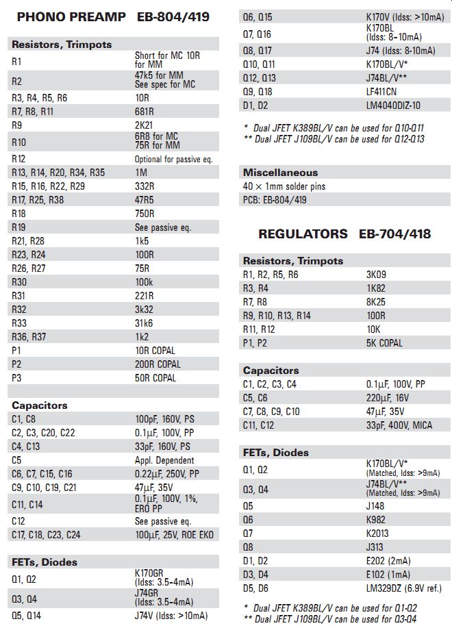
PHONO PREAMP EB-804/419
Resistors, Trimpots R1
Short for MC 10R for MM R2 47k5 for MM See spec for MC R3, R4, R5, R6 10R R7, R8, R11 681R R9 2K21 R10 6R8 for MC 75R for MM R12 Optional for passive eq.
R13, R14, R20, R34, R35 1M R15, R16, R22, R29 332R R17, R25, R38 47R5 R18 750R R19
See passive eq.
R21, R28 1k5 R23, R24 100R R26, R27 75R R30 100k R31 221R R32 3k32 R33 31k6 R36, R37 1k2 P1 10R COPAL P2 200R COPAL P3 50R COPAL Capacitors C1, C8 100pF, 160V, PS C2, C3, C20, C22 0.1µF, 100V, PP C4, C13 33pF, 160V, PS C5 Appl. Dependent C6, C7, C15, C16 0.22µF, 250V, PP C9, C10, C19, C21 47µF, 35V C11, C14
0.1µF, 100V, 1%, ERO PP C12
See passive eq.
C17, C18, C23, C24 100µF, 25V, ROE EKO FETs, Diodes Q1, Q2 K170GR (Idss: 3.5-4mA) Q3, Q4 J74GR (Idss: 3.5-4mA) Q5, Q14 J74V (Idss: >10mA) Q6, Q15 K170V (Idss: >10mA) Q7, Q16 K170BL (Idss: 8-10mA) Q8, Q17 J74 (Idss: 8-10mA) Q10, Q11 K170BL/V* Q12, Q13 J74BL/V** Q9, Q18 LF411CN D1, D2 LM4040DIZ-10
* Dual JFET K389BL/V can be used for Q10-Q11
** Dual JFET J109BL/V can be used for Q12-Q13
Miscellaneous
40 × 1mm solder pins PCB: EB-804/419 REGULATORS EB-704/418 Resistors, Trimpots R1, R2, R5, R6 3K09 R3, R4 1K82 R7, R8 8K25 R9, R10, R13, R14 100R R11, R12 10K P1, P2 5K COPAL
Capacitors
C1, C2, C3, C4 0.1µF, 100V, PP C5, C6 220µF , 16V C7, C8, C9, C10 47µF, 35V C11, C12 33pF, 400V, MICA
FETs, Diodes Q1, Q2 K170BL/V* (Matched, Idss: >9mA) Q3, Q4 J74BL/V** (Matched, Idss: >9mA) Q5 J148 Q6 K982 Q7 K2013 Q8 J313 D1, D2 E202 (2mA) D3, D4 E102 (1mA) D5, D6 LM329DZ (6.9V ref.)
* Dual JFET K389BL/V can be used for Q1-Q2
** Dual JFET J109BL/V can be used for Q3-Q4
--------
[The discussion above is adapted from an article, Jul 2005, outlined in xyz ]
Also see: