USB Audio: PC Sound Amp
--------
By Jeno Keceli
No extra sound card is required for this PC sound amplifier, which gets its signal via the USB port.
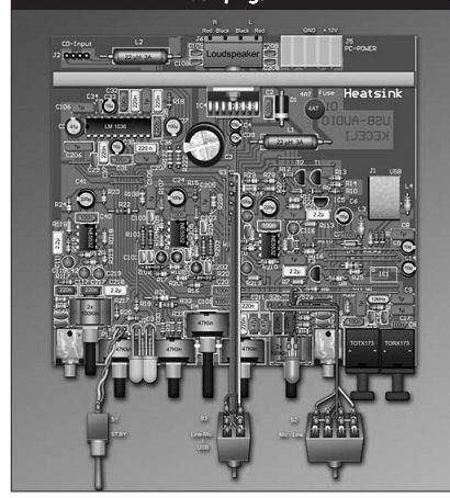
PHOTO 1: Completed audio amp. There is a hole on the heatsink for the USB
plug.
Nowadays there is a sound card in every PC, which, in most cases, has only analog connectors. In this interface the signal is applied to the sound amplifier. These two units (the sound card and the sound amplifier)--together with the S/PDIF connectors--are mounted on a board inside the computer chassis. This way there is neither external cabling nor an external amplifier; the amp is powered by the computer itself.
Figure 1 shows the block diagram of the USB audio equipment. You can see that a USB audio codec IC provides the A/D conversion. Universal implementation is enabled by S/PDIF (fiberoptic) and analog connectors; which substitute for the sound card.
IC1 performs the communication functions with the computer and also is responsible for the D/A conversion.
This is followed by IC2, the low-pass filtering stage, which is used for filtering components that result from the conversion. IC3 is responsible for regulation--volume and tone control.
Finally, the power amplifier, IC4, amplifies the signal.
I added some more components that enable universal use of the device. The audio codec IC1 is connected to IC8 and IC9, which are fiberoptic (S/PDIF) interfaces; the analog signal is available from the line output. The output level is set by the P6 potentiometer, which you can adjust by using a screw driver. IC7 functions as a signal buffer. By setting the S2 switch, you can select the analog microphone or the line input for recording. The recording level is regulated by P5; its amplification is achieved through IC6. With the S3 switch you can choose between the USB input and the analog input (monitor).
THE APPLIED PCM2902
The PCM2902 is a single-chip USB stereo audio codec with a USB 1.1 com pliant full-speed protocol controller with single-ended analog input/output and S/PDIF. The USB protocol controller works with no soft ware code.
Figure 2 shows the functional block diagram of PCM2902. The decoded out put signal appears on both the S/PDIF and the analog outputs. The input sound signal (Record) is selected automatically as either S/PDIF or analog input.
When S/PDIF is detected, it will be active because it has the higher priority.
If the digital signal is not present, the analog input will be activated. Because the applied IC has copyright-detection circuitry, the copyright-protected signal cannot be transmitted through S/PDIF. The IC detects this and switches to the analog input. The analog input has fixed sensitivity--it cannot be regulated--but ...
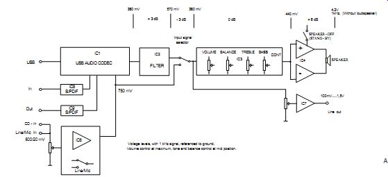
FIGURE 1: Block diagram (voltage levels, with 1kHz signal, referenced
to ground. Volume control at maximum, tone and balance control at mid-position).
... due to the AD converter it depends on the VCCCI voltage. In this case it is approximately 750mVeff, (VCCI = 3.5V). The analog output can be regulated through the IC or the software program
----------------
Main Features of PCM2902 (for more details see the product manual)
-Fully compliant with USB 1.1
-Bus powered
-16-bit delta sigma ADC and DAC
-Sampling rate: DAC: 32, 44.1, 48kHz,
-ADC: 8, 11.025, 16, 22.05, 32, 44.1, 48kHz
-On-chip clock generator: 12MHz
-Single power supply: 5V (VBUS)
-Stereo ADC analog performance:
THD+N = 0.01%, SNR = 89dB, dynamic range = 89dB
-Stereo DAC analog performance:
THD+N = 0.005%, SNR = 96dB, dynamic range = 93dB
-Volume and mute control
-Suspend flag
------------
USB Audio Amplifier Test Results
Supply voltage amplifier: +12V from PC Supply voltage USB codec +5V from USB bus Current drain (amplifier): approximately 120mA (idle), approximately 3.5A (full power) Current drain (USB codec): approximately 90mA Output power: 2 × 20W @ 4 , musical, 2 × 15W (THD 0.5%) Frequency response: 20 Hz . . . 20kHz, + 0.5 . . . -2dB Line input, 600mV input impedance 120k-ohm
Electret mike input 20mV microphone supply Line output, max 1.5V (cca -15. . . +10dB) from preamplifier (adjustable with a screwdriver) S/PDIF input and output Power output shorting and overheat protection control Standby switch, volume (built-in contour), tone and balance control on the front panel Size: front panel 148 × 42mm (similar to a CD-ROM), depth 135mm
----------
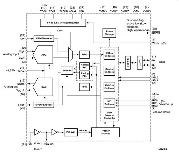
FIGURE 2: PCM 2902 functional block diagram.
-------
... as well. Internal analog power supply for codec VCCCI = 3.3V.
In order to increase the quality of the AD conversion, the manufacturer recommends slightly increasing the VCCCI (e.g., VCCCI = 3.5 ... 3.65V) with a separate voltage regulator. The analog in- and output signals have approximately +1.7V DC superimposed, which enables direct connection to rail-to-rail operational amplifiers. (However, in this case, this feature is not utilized.)
PRINCIPLES OF OPERATION
Figure 3 shows the amplifier's detailed schematics. There is duplex communication on the USB connector; this is connected to IC1, where--after the identification--the connection is made and the con version of D-A/A-D starts to function.
Because IC1 has a suspended output as well, this can be used for external switching control. In this case an LED is applied through T3. When the connection is achieved the LED switches off. Active LED means that the connection with the computer has not been established.
The frequency of the quartz oscillator is relevant for the establishment of the connection. Because the parallel resonance capacity of various quartz types may differ, the connection might become difficult to establish or unstable. If this happens, you need to modify the capacitors C15 and C16. According to the manufacturer the appropriate value should be between 10-30pF. With a standard 12MHz HC18 used, I found 15pF to be the optimum value. When working with an SMD quartz you will probably need a higher value of C15/16.
After establishing the software connection, the sound-frequency signal appears on outputs 15 and 16, but it also appears on output 25 as digital signal (DOUT), which is applied to IC9 as S/PDIF connector.
IC8 is another S/PDIF connector serving as a digital input for recording, but there is an analog input (pin 2 and 3) as well. The input is automatically selected in IC1. If the digital signal (DIN) is absent, the analog input will be activated (VINR, VINL). The appearance of the digital signal causes a switchover.
IC1 is copyright-protected against illegal reproduction (Serial Copy Management System SCMS). If a copied signal is discovered on the digital input, IC1 will switch to the analog input, preventing the production of perfect digital copies.
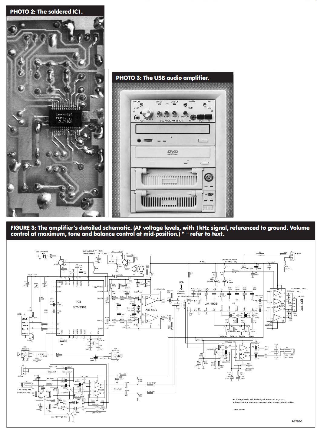
PHOTO 2: The soldered IC1.
PHOTO 3: The USB audio amplifier.
FIGURE 3: The amplifier's detailed schematic. (AF voltage levels, with 1kHz signal, referenced to ground. Volume control at maximum, tone and balance control at mid-position.) * = refer to text.
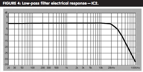
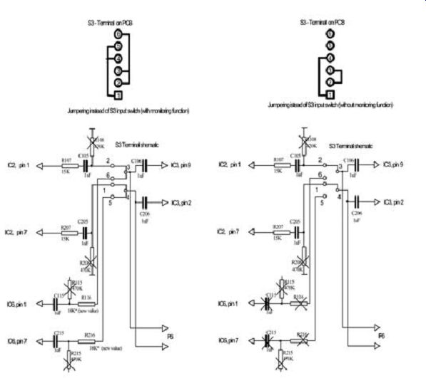
FIGURE 4: Low-pass filter electrical response -- IC2.
FIGURE 5: Switch S3 can be eliminated. Variations: S3 terminal and PCB, jumpering instead of the S3 switch (keeping the monitoring function). Here, resistors R108, R208, R115, and R215 become superfluous. R116 and R216 are changed for 18k. S3 terminal and PCB, jumpering instead of the S3 switch (eliminating the monitoring function). The following components become unnecessary: C115, C215, R115, R215, R116, R216, R108, and R208. S3 terminal schematics, new value.
PHOTO 4: USB audio amplifier, front side. PHOTO 5: USB audio amplifier, back side.
The sensitivity of the analog input is permanent (approximately 750mV), and software regulation is not possible. Since the ADC has an on-chip anti aliasing filter, the input circuit is quite simple. However, to ensure good audio quality, MKT (Siemens) or equivalent capacitors are specified for positions C101, C201, and C110, C210. Do not use electrolytic capacitors here.
The volume regulation provided by IC1 has not been utilized, as it is identical to the software regulation in the computer. IC1 is powered with +5V VBUS from the USB bus. For filtering disturbances two inductors, L3 and L4, have been installed here. Further filtering is assured by capacitors C6 and C7.
The PCM 2902 has an on-chip volt age regulator. On pin 10 the voltage is:
VCCCI = 3.3V (internal analog power supply for codec).
The circuit functions well with this voltage, but according to the manufacturer's recommendations, the distortion can be somewhat reduced if you slightly increase the voltage with the IC5 voltage stabilizer. Here, a volt age regulator type LM317 is used. Its presence reduces harmonic levels by more than 10dB as compared to the internal voltage regulator. Note that IC1 itself provides excellent quality--you cannot hear the impact of the voltage increased by an external stabilizer.
Accordingly, you can omit IC5, but you must apply the filter capacitor C5 belonging to it. Because LM317 is sup plied from 12V--in case of the absence of the 5V VBUS (USB out)--IC5 must be switched off, otherwise the identification cannot be completed when reconnecting to the USB. This is achieved by transistors T1 and T2. If the 5V is present on diode D4, the 12V has a free path as well. If the 5V is absent, the 12V is switched off the IC5.
SIGNAL FUNCTION
In IC1 the ADC has an on-chip antialiasing due to noise shaping. To eliminate the various distortion products, you must apply a third-order Butterworth low-pass filter with fc = 28kHz. The amplifier IC2 is realized by an op amp type NE5532. The signal at the DAC output may be slightly amplified (1.5 times). The virtual ground (+6V)--filtered by C25 capacitor--is generated by resistors R16, R17, R101, and R201. This is necessary for setting the op amp bias.
Figure 4 shows the low-pass electrical response.
The signal from the filter IC2 goes to the input signal selector S3, through capacitors C105, C205 and resistors R107, R207, which reduce the unnecessary gain. If you change R107 and R207, the (input sensitivity) gain may change.
DC null potential is produced by R108, R208, R115, and R215. This is necessary for preventing the switchover click.
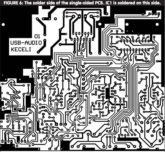
FIGURE 6: The solder side of the single-sided PCB. IC1 is soldered on this
side.
A switch does input selection; this way the signal reaches the tone control stage. IC3 carries out the tone control task. Its gain is 0dB and cannot be altered. Besides the bass and treble tone control, the volume and balance control are also here. This is a complex stage; DC levels carry out the control.
From the point of view of construction, this makes the stage less complicated because the RC items of the usual tone control stage are not required, and mono potentiometers are sufficient for the control.
IC3 also contains a loudness tone correction stage. This is important when the volume is low because it sets the sound transmission to the sensitivity of the human ear. In our case, this stage is always switched on. You can switch it off for experimenting if you switch off pin 7 from pin 12, and switch it over to pin 17.
After setting the frequency response, the signal goes to the power stage through C107, C207 capacitors. IC4 per forms the power gain. For this, I have chosen an item that requires only a few external components that still can produce good quality.
The gain of the TDA 7375 is set at 26dB. According to the manufacturer's specifications, the inverted and non inverted inputs of the IC are joined together. The inverted inputs provide phase-shifted signal, which is required for the functioning of the bridge circuit.
In this way no separate phase inverter is required.
As I have already mentioned, TDA 7375 IC has a standby pin that is connected to the switch on the front panel.
Shutting down the whole amplifier is not possible, but you can switch off the loudspeakers with the standby switch.
Because the other stages of the amplifier operate independently of this, you can listen to the music through the line output. J6 terminal block is the loudspeaker connector on the PCB, but only for internal connection, because the loudspeaker connector is on the back panel of the computer. Propagation of interfering signals is minimized by capacitors C108, C109, C208, and C209.
ADDITIONAL MODIFICATIONS
The amplifier is able to function now, but for the sake of general implementation, I applied two more ICs. IC7 pro vides a line output signal from the pre-amplifier. This output can serve as a PA-driver or line output. The circuitry of the stage is conventional. IC7 has mini mal gain, the output level is adjustable (using a screwdriver) with the P6 that is on the front panel. The virtual ground (+6V) is produced by R23, R24, R120, and R220, and is filtered by capacitor C42. As protection against the impact of capacitive load, resistors R117, R217 are installed. The output is filtered by C118, C218. The connector J7 is found on the front panel of the PCB.
IC6 is a preamplifier. Because there is no software solution for setting the input (Rec) level, a potentiometer P5 has been installed. The terminal block J2 is a CD audio input--placed on the inner side of the PCB--functioning as inner connection primarily for listening. Connector J3--on the front panel--functions as a line or an electret microphone input. Besides the monitoring function, you can also use this input for recording, making phone calls, and so on. You can switch between line and microphone input with the switch S2b controlling the gain of the stage that is the input sensitivity. The electret micro phone is supplied from resistors R34, R35, and is filtered by capacitor C19.
R114 and R214 are the ballast resistors.
Resistors R28, R29, R110, and R210 produce the virtual ground (+6V), which is filtered by electrolyte capacitor C20. Because of the higher gain, this stage should be neutralized by capacitors C122, C222, avoiding buildup. The task of capacitors C112 and C212 is high-frequency filtering.
The amplifying stages are supplied by +12V from the computer through connector J5. Filtering is done by inductor L1 and capacitors C2 and C3.
Diode D1 provides protection against over-voltage.
As there is ground connection from the USB connector side as well, this can be a noise source. This is why two more inductors, L4 and L2, have been installed, suppressing all kinds of noises. The power supply of each stage is filtered, too. This is done by R27, C22, C21 (preamplifier), R22, C41, C40 (line output), R18, C26, C27 (control unit), and R15, C23, C24 (filter).
You can omit switch S1 by simply jumping the switch--if no standby function is needed. As a result, you can also ...
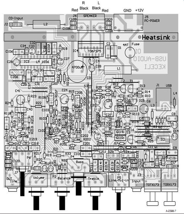
FIGURE 7: Parts placement, components side. IC1 is on the soldering side
of the PCB.
-------------------

TABLE1: Parts List of the USB Audio Amplifier.
SCHEMATIC REFERENCE PART TYPE CASE/ DESCRIPTION DESIGNATOR VALUE LEAD PITCH IC1 PCM2902 JEDEC MO-150 SMD IC2, IC6, IC7 NE 5532 DIP-8 IC3 LM 1036 DIP-20 IC4 TDA7375 IC5 LM317 TO-92 IC8, TORX173 IC9 TOTX173 D1 1.5 KE 15A 15.24 Protection- suppression diode D2, D3 LED 2.54 standard D4 ZPD 3.6 7.62 D5 LED 2.54 low current, red T1, T2 BC547 TO-92 T3 BC556 TO-92
C2 100nF
5.08 MKS, MKP, ceramic C3 4700µF 7.62
Electrolytic-radial C4, C5, C6, C14, C25, 10µF 2.54
Electrolytic-radial C30, C33, C39, C121, C221 C7, C17, C18, C23 100nF 2.54 MKS, MKP,
ceramic C8, C9, C10, C11, C105, 1µF 5.08 MKS, MKP C106, C107, C115, C205, C206, C207, C215 C15, C16 15pF 2.54 Ceramic C19, C27 100µF 2.54 Electrolytic-radial C20, C42, C116, C119, 6.8µF 2.54 Tantalum C216, C219 C21, C201 100nF 5.08 MKS, MKP,
ceramic C22, C41 220µF 5.08 Electrolytic-radial C24 100µF 5.08 Electrolytic-radial C26, C35, C36, C37, 220nF 5.08 MKS, MKP C38, C111, C113, C117, C211, C213, C217 C28 47µF 2.54 Electrolytic-radial C29, C34 10nF 2.54 Ceramic C31, C32 390nF 5.08 MKS, MKP C40, C101 100nF 5.08 MKS, MKP, ceramic C102, C202 1.5nF 2.54
Ceramic C103, C203 1nF 2.54
Ceramic C104, C204 470pF 2.54 Ceramic C108, C109, C208, C209 100pF 2.54 Ceramic C110, C118, C210, C218 2.2µF 5.08 MKS, MKP C112, C120, C212, C220 47pF 2.54 Ceramic C114, C214 0.47µF 5.08 MKS, MKP C122, C222 220pF 2.54 Ceramic Q1 12MHz 5.08 Quartz L1, L2 22µH/3A Axial Inductor
SCHEMATIC REFERENCE PART TYPE CASE/ DESCRIPTION DESIGNATOR VALUE LEAD PITCH
L3, L4 1.5µH 7.62 Axial L5 47µH 7.62 Axial R1, R2, R15, R18, R22, 22 ohm
5.08 ¹/8W R27 R3, R34 1.5k 5.08 ¹/8W R5 1M 5.08 ¹/8W R6, R19, R20 1k 5.08 ¹/8W R7, R111, R113, R118, 33k 5.08 0.25-W R211, R213, R218 R8, R16, R17, R21, 100k 5.08 ¹/8W R23, R24, R28, R29, R110, R120, R220 R9 4k 5.08 ¹/8W R10 6.36k 5.08 ¹/8W R11 560 ohm
5.08 ¹/8W R12, R30, R31, R32, R33, 47k 5.08 ¹/8W R109, R122, R209, R222 R13, R14, R105, R114, 10k 5.08 ¹/8 W R119, R205, R214, R219 R25 4.7 ohm
5.08 ¹/8W R26 8.2K 5.08 ¹/8W R35, R121, R221 4.7k 5.08 ¹/8W R101, R108, R115, R201, 470k 5.08 ¹/8W R208, R215 R102 5.6k 7.62 ¹/4W R103 6.81k 7.62 ¹/4 W R104 6.65k 7.62 ¹/4W R106, R206 22k 5.08 ¹/8W R107, R207 15k 5.08 ¹/8W R112, R212 470 ohm
5.08 ¹/8W R116, R216 39k 5.08 refer to text R117, R217 100 ohm
5.08 ¹/8W R202 5.6k 5.08 ¹/8 W R203 6.81k 7.62 ¹/8W R204 6.65k 5.08 ¹/8W R210 100k 7.62 ¹/2W P1, P2, P3, P4 47 k-ohm
Potentiometer PCB mounted P5, P6 2×100k-lin Potentiometer PCB mounted S1 Subminiature on-off panel mounting
toggle switch S2 Subminiature 4 pole on-on panel mounting
toggle switch S3 Subminiature 2 pole on-on panel mounting
toggle switch F1 mini T4.0A
FUSE J1
USB connector B type panel mounted J2, J6
Terminal block 4pin PCB mounted J3, J7
Phone-jack
Socket PCB
PCB mounted
3.5mm stereo J5 PC power 4 pin, male PCB mounted
connector PCB 104 × 86mm Single-sided
---------------------------
... omit R20 and D2 LED. If the electronics is modified according to Fig. 5, switch S3 can be eliminated, as well.
By the first solution--jumping the switch--you add up the signals. The monitoring function is there, but for preventing interferences only one input is used at a time. Here, resistors R108, R208, R115, and R215 become unwanted. R116 and R216 are changed to 18k.
By the second solution, there is no monitoring function, as--omitting the switch--the signal is applied from the USB input. The following components become unnecessary: C115, C215, R115, R215, R116, R216, R108, and R208.
CIRCUIT ASSEMBLY
The PCB is a single-sided board; Fig. 6 shows the soldering side. With the exception of IC1, all the components are installed on one side. The installation of the components is illustrated in Fig. 7. For the sake of simplicity I have chosen conventional components that can be soldered in without complication.
The only exception is IC1 PCM 2902, which is available only in SMD 28-Pin Flatpack (SSOP 28) and is very tiny. For soldering this component you need a precision soldering iron, a magnifying glass, experienced, calm hands, and good eyesight. The thickness of the pin and the distance between the pins is approximately 0.3mm, or 12 Imp. These cannot be soldered in by casual methods.
First, you must install this component. To do so you should cover the PCB around the IC with a thin layer of sol der. Check to see whether there is a bond--there should not be. Antistatic precautions should be observed in handling the IC. Excessive static electricity is harmful for it, hence neutralization of the static build-up is a must. Your working surface should be conductive and you should use an antistatic wristband tied to the working surface. Also, connect the neutral of the soldering iron to the conductive surface. The wristbands are regularly available from hobby or electronics component shops.
Check all the pins--under no circum stances should they be bent, and it is important that they should be on the same plane. Then place the component on the PCB and adjust its exact position. To fix it, solder in—diagonally--two opposite pins or--even better--stick it down with SMD glue. The difficult part of the assembly is yet to come.
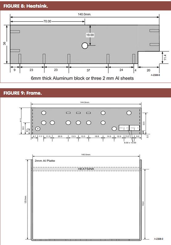
FIGURE 8: Heatsink.
FIGURE 9: Frame.
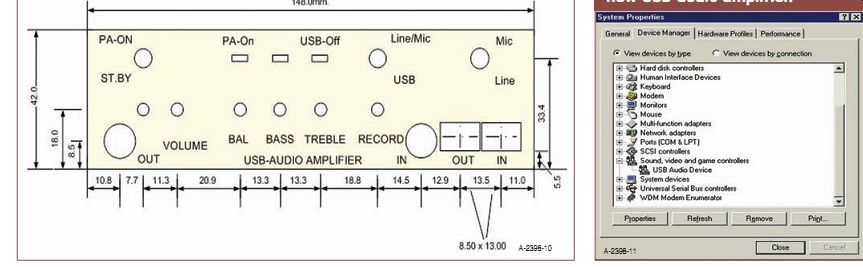
FIGURE 10: Front panel.
FIGURE 11: The PC recognizes the new USB-audio amplifier.
The pins must be soldered in one by one with a needlepoint soldering iron--not putting any extra tin on it (what you used for covering the IC on the PCB is enough). Pull the soldering tip from the outside toward the IC--through the cop per foil--melting the tin up to the IC pin. This melted tin solders the pins.
After soldering in the 28th pin, check your work in detail under a magnifying glass. The work is only then perfect if you check all the pins--one by one--for break age and/or bridges between pins and no fault is found. (You can use sewing needles as test probes.) Photo 1 shows the soldered IC1. Solder in the other components that belong to IC1 and the USB part, then test the circuitry. If the identification is unstable, modify the C15, C16 capacitors. When the computer recognizes the USB codec, the LED D5 switches off. The rest of the assembly is nothing unusual.
The heatsink is prepared according to Fig. 8. It can be made of a 6mm thick aluminum (Al) block or three 2mm Al sheets which are bound tight together with screws to form a single block. Cut a hole for the USB jack. If the work has been well done, no further adjustment is needed; the equipment is ready for operation. To fasten it, place the PCB in a frame made of a 2mm Al sheet that has been prepared according to Fig. 9. A front panel, illustrated in Fig. 10, hides the screws and components, but this has only an esthetic function.
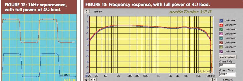
FIGURE 12: 1-kHz squarewave, with full power at 4 ohm load.
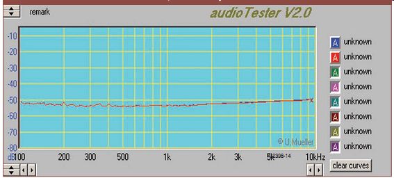
FIGURE 13: Frequency response, with full power at 4 ohm load.
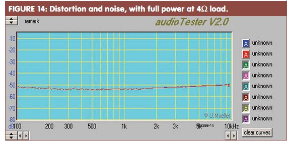
FIGURE 14: Distortion and noise, with full power at 4 ohm load.
AMPLIFIER ASSEMBLY
Assembling the amplifier is easy, no adjustment is required. If you work carefully and avoid mistakes, the amplifier will work at once. After having tested what you have built so far, you can install the amplifier.
Warning: while installing and connecting equipment inside the PC, be sure the PC is switched off.
Connection of the amplifier to an operating PC might cause a system crash due to the charging current and the high capacity of C3. The USB audio module receives the signal through a USB cable from the PC. A ferrite bead functions as a filter on this cable. You can install a similar ferrite bead on the loudspeaker cable as well. In order to avoid short circuits, it is advisable to place an insulating sheet below the amplifier.
SOFTWARE INSTALLATION
Problems are unlikely to occur with the installation of the board under Windows. First there comes a notification that a "USB Audio Codec" has been found, which requires drivers to be installed. Then the following three devices are found: a "USB Composite Device," a "USB human Interface Device," and a "USB Audio Device." These items are located under the Sys tem Properties/Device Manager tab (Fig. 11). Next, with Playback properties you will see three slide controls: Desktop, Wave, and SW Synth.
The fourth slider CD Player (for Windows' own simple software player for audio CDs) will be missing and will be available only after the computer is restarted. In Control Panel, under the Multimedia/CD Music tab, remember to check "Enable digital CD audio for this CD-ROM device." If the USB link is briefly interrupted, the control may disappear. This is normal (for Windows, at least) and results due to a bug in the operating system. The problem has not been solved under Windows ME or XP, which apply different names for some of the windows and controls.
TEST
The voice frequency circuitry is tested by casual measurements, but the USB codec expects the presence of an operating computer as well. Because there are usually no adequate instruments available for amateurs, it is a good idea to use the Internet for help.
You can find various audio tester pro grams on the Internet to test the full USB audio transmission line. I applied the software program found at the website sumuller.de.
You can download this program for 30 days' evaluation. As for the complete testing of the full duplex operational mode, apply a conventional soundcard as input and the newly built equipment as output. Their selection is done in the Windows audio program. The test results are shown in Figs. 12, 13, and 14.
---Jeno Keceli is a long-time electronics enthusiast with 40 years of experience. His main fields of interest are designing and building tube and transistor power amplifiers. He has much experience with sound and disco equipment. His articles have been published in electrotechnical journals. He now runs his own firm, where he builds, repairs, and gives advice. Email: kecelijeno@freemail.hu. ---
REFERENCES
PCM2902 Burr-Brown Products from Texas Instruments, Specification publication
NE5532 Texas Instruments Production data information
TDA 7375A STMicroelectronics Specification publication
LM1036 National Semiconductor Production data information
TORX173 Toshiba Fiber Optic Receiving Module, Production data information TOTX173
Toshiba Fiber Optic Transmitting Module, Production data information
"USB Audio Codec with S/PDIF," Elektor Electronics, 12/2002
"USB-Digital-Soundmodul" ELV Journal, 4/2003 AudioTester software sumuller.de
--------
[The discussion above is adapted from an article, Jul 2005, outlined in xyz ]
Also see: