National Semiconductor’s LM4702 meets up with Renesas lateral MOSFETs.
National Semiconductor has been fast at work designing analog products for the high-end audiophile market. As fortune would have it, these products such as the LM4780 Power Amplifier Chip and the LM4702 Driver Chip are easy to implement into high-quality designs for the audio DIYer.

National recently introduced the LM4702, a high-voltage driver chip that interfaces bipolar or MOSFET output devices. The LM4702 provides two small signal, input stages and voltage amplification stages (VAS). All you need to do is design a suitable bias system and output stage.
Not to be outdone in making the job easy for us amateurs, National provides a comprehensive design outline, guide to printed circuit board construction, ideas for the power supply, bill of materials, and suggested layout. In an application note dated May 20061, the company described an amplifier using high-quality construction techniques and off-the- shelf passive components. The result is an amplifier with a vanishingly low level of distortion, 0.0006%.
The amplifier described here comes close to achieving the performance stats described by National, but this DIYer has neither a Faraday shielded room nor Audio Precision distortion analyzer with which to squeeze the last iota out of performance. At 1kHz, 10W into 8 THD+N is around 0.004%. You can probably assemble the amplifier for $150, with the bulk of the expense going towards a suitable power transformer and chassis in which to house the device.
PICKING UP WHERE NATIONAL LEAVES OFF
The LM4702 is limited by its ability to sink or source a maximum current of 10mA from source to sink pins. As a result, output bipolar devices must use a Darlington configuration for the kinds of output power which now seem de rigueur. Nevertheless, National hints in their literature at the possibility of using MOSFET output devices, suggesting that those with low turn-on voltages might be appropriate in such an application.
Picking up on this idea, I designed a very high-quality amp that uses lateral MOSFETs from Renesas as the output devices. Lateral MOSFETs enter into their linear phase at a lower bias voltage than vertical MOSFETs and are well- suited for the task.
THE LM4702 DRIVER
The LM4702 driver (Fig. 1) provides two sets of input and VAS stages. As with the Overture series LM3886 and LM4780, the device also provides a mute function. The chip requires external compensation; for the circuit in this article I use 30pF silver mica capacitors, as did Brasfield in his application note.
National leaves the method of biasing the output devices to the end user. In this case I have employed a VBE multiplier with a PNP device, the MPSA56. The schematic (one channel) of the completed driver for the amplifier is shown in Fig. 2.

FIGURE 1: The LM4702.
In many respects the input and VAS stages of the amplifier do not differ from the high-performance unit described in National’s application note. The lateral MOSFETs require a few tricks to keep from oscillating, however. In this case I placed 330pF ceramic capacitors on each of the n-channel devices from gate to source and compensated the feedback loop by bypassing the feedback resistor with a 10pF capacitor, C14 in series with a 33 ohm resistor across the feedback resistor (R1). In one iteration of testing the amplifier, I placed 47pF and 22pF mica caps from drain to gate on the 2SK1058 and 2SJ162 output transistors, but found the prior setup to provide the best balance between power bandwidth and distortion.
The LM4702’s supply lines are de coupled with 10 ohm resistors (R1, R24) to tweak the performance a bit. The author of the application note pointed out that you could omit capacitors C6 and C7 for critical listening input. If you do this, however, a servo might be necessary to prevent DC from appearing on the output. Local power pin decoupling is important with the LM4702.
I used 470nF polypropylene capacitors for C1, C2, and C13 because I had these on hand. I placed capacitor C2 across the power input pins of the printed circuit board. Diodes D1-D4 protect the devices from gate-source breakdown. For simplicity sake I have shown a SPST switch used to control the LM4702’s mute pin. One to two milliamps should flow into this pin to bring the amp out of mute. The output stage schematic is shown in Fig. 3.
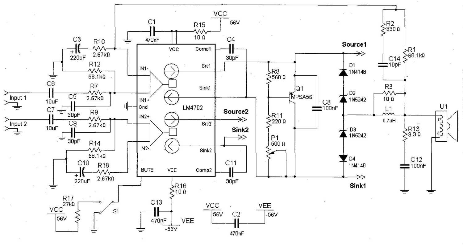
FIGURE 2: The schematic of the completed driver (one channel).
POWER SUPPLY
The power supply used for the amplifier is fairly straight forward, employing a 400VA transformer, On-Semi MUR860 diodes, and 39,000 capacitance for each rail. Both AC inputs to the power transformer are switched and fused. In my amplifier I filtered the AC input with a Corcom 10VK1 filter. This takes up little space and will handle the current demands without difficulty. The filter keeps electromagnetic and radio interference from propagating into the power supply and amplifier circuitry.
I use General Electric CL-30 inrush current limiters to protect the diodes. Resistors R2 and R4 discharge capacitors C5, C6 in a period of several minutes. Given the large capacitors used, it will take a few minutes to filly discharge C5 and C6 by 99%. You can use the auxiliary regulated voltages to drive speaker protection circuitry, a DC servo, or crossover if you think this is necessary.
A typical diode snubber circuit is illustrated in Fig. 4 for those concerned about diode switching noise. The values of R and C in the snubber depend upon the secondary leakage inductance of transformer Ti. A discussion of the values and the necessity of diode snubbers is contained in “Calculating Optimum Snubbers,” which you can find on Jim Hagerman’s website hagtech.com.
Note: As described, I used 39,000uF 80V DC capacitors in the LM4702 power supply. Each of these capacitors is tested prior to shipment and may contain a residual charge. This could cause a nasty little shock if you are not careful in handling the devices.

FIGURE 3: The output stage.

FIGURE 4: A typical diode snubber circuit. Suggested Line Filter; Suggested
Diode Snubber
PRINTED CIRCUIT AND LAYOUT
I originally designed the printed circuit board incorporating both driver and output devices and used this design for the testing and performance data found at the end of this article. For ease of use, however, this article includes a printed circuit board design that separates the driver and output boards. This will allow much higher power designs, the use of lateral or vertical MOSFETs, or bipolar Darlington devices if you so choose.
National recommends that you keep the layout as symmetrical as possible, and my performance tests over the course of several months convinced me that this discipline will improve the amplifier’s performance by several thousands of a percent of THD. No ground plane is shown, and it is National’s recommendation not to include one in your design if you want the best performance.
To simplify the connection of the power supply leads, I ran a #12 stranded wire from the front to back of the printed circuit board. Otherwise, the power, output, and speaker ground traces at 200mils seem to be adequate for the job. Figures 5-7 show the bottom, silk screen, and top printed circuit board images in respective order (although reduced to save space). The Gerber files are available for free download at www.audio-Xpress.com.

FIGURE 5: LM4702 driver board bottom.

FIGURE 6: LM4702 driver board silkscreen.
COMPLETED AMPLIFIER MODULE
Photo 1 shows the completed amplifier module used for the testing. There is sufficient space given between the transistors to distribute the heat across the sink
To the greatest extent possible, I have maintained symmetry between the two channels of the amplifier. You could certainly consider different part orientations, particularly if you want to place the output devices on the rear of an amplifier chassis. This layout, however, allows for the placement of two large heatsinks on the right- and left-hand sides of the chassis.
I strongly recommend using a TO- 220 heatsink on the LM4702. I have found that as the chip warms up, the harmonic distortion of the amplifier will tend to increase as the internal temperature of the amplifier rises. Under certain circumstances the LM4702 will thermally cycle if it isn’t heatsinked.
SETUP AND OPERATION
The amplifier is pretty easy to set up. (A Variac is helpful, however.) Short the input connectors to ground and bring up the line voltage. ‘With a voltmeter, measure the voltage across the 0.22 ohm source resistors. Adjust the potentiometers for 22mV of voltage for each device. This equates to 100mA of bias current. I let the amplifier cook for another 15 minutes and check the bias to make sure it hasn’t wandered.
PERFORMANCE
The LM4702 driven MOSFET amplifier performs quite well. While I was unable to attain the remarkable 0.0006% that National demonstrated in application note 1490, the lateral MOSFET doesn’t seem to get into quite as much trouble at high power levels. For comparison purposes, at 10W output power the lateral MOSFET amplifier exhibited THD of 0.004%, while the bipolar Darlington unit from National displayed 0.001%.

PHOTO 1: The completed amplifier module used for testing.
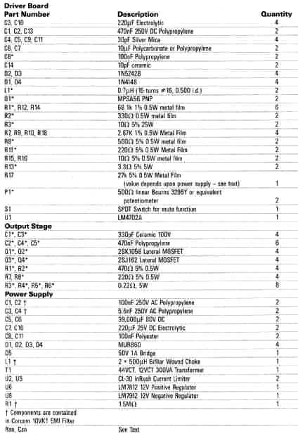
PARTS LIST
(Part Numbers relate to the schematics, but the quantities for those parts with an asterisk represent the quantities necessary for two channels)
The test setup consisted of both Tektronix SG505 and AA501 and Boonton 1120 Distortion Analyzers, a Hewlett-Packard HP 3577 Network Analyzer, Tektronix TDS3012B oscilloscope, and an 8 ohm resistive load. The maximum power that I was able to attain from the amplifier as shown was a continuous 150W at which level it expressed its unhappiness with me.
The plot of total harmonic distortion versus power at 100Hz, 1kHz, and 10kHz is shown in Fig. 8. Power band width, from 10kHz to 100kHz, is illustrated in Fig. 9.
PARTS LIST
Most of these components are available from the usual sources including Digi-key, Mouser, Allied, Jameco, and so on. You can use the Hammond 182P22 225 VA rated transformer (available from Digi-key and Mouser) as long as you don’t use the amp to drive servo motors or some industrial load. A heavier duty imported transformer is available from Antek, in North Arlington, N.J. Their AN3240 is rated 300 V.A. for continuous industrial service in servo use. (Antek is an ISO-9001 rated company serving the CNC industry.) Their AN3240 is rated 300VA for continuous industrial service in servo use. You can purchase Antek’s transformers from their website, www.toroid-transformer.com.
It is important that the line capacitors C1, C2, C3, and C4 be rated for AC operation. High quality 250V AC polypropylene X and Y capacitors should be used in these positions unless you use the Corcom 10KV1 EMI Filter.

FIGURE 8: Plot of total harmonic distortion vs. power at 100Hz, 1kHz, and
10kHz. LM4702 Driver Lateral MOSFET Amplifier

FIGURE 9: Power bandwidth from 10kHz to 100kHz. Power Bandwidth.
REFERENCES
1. Brasfield, Mark, “LM4702 Amplifier National Semiconductor Corporation Application Note 1490,” National Semiconductor Corporation, Santa Clara, CA, 2006.
2. Hagerman, Jim, “Calculating Optimum Snubbers,” The Audio Amateur 3/94.
[The discussion above is adapted from an article outlined in xyz Jul. 2007]
Also see: