Up until about ten years ago, the choice when designing a high power audio amplifier was between bipolar transistors or valves. Even in those days, the valve option was not a popular one. Whatever the relative merits of valves and transistors in high power audio applications (and valves do have their advantages where high powers are involved), valves were not a popular choice due to difficulties in obtaining the necessary components. These days the component buying problems are that much greater, rendering home constructed valve amplifier projects something that are only suitable for the dedicated few.
These days there is a real alternative to bipolar transistors in the form of power field effect transistors (f.e.t.s). The two commonly available forms of power f.e.t. are the VMOS and the power MOSFET types. High power VMOS transistors suitable for operation in high power audio amplifiers are produced, but these are not very readily available. Also, complementary devices suitable for genuinely symmetrical class B output stages are very difficult to obtain. Quasi-symmetrical output stages using only n channel devices (the f.e.t equivalent to n.p.n. bipolar transistors) are possible, but the lack of true symmetry can compromise performance.
For audio applications the Hitachi power MOSFETs are probably the better choice. These are somewhat more expensive than VMOS devices, and are substantially more expensive than most bipolar power transistors. On the other hand, they have high voltage, current, and power ratings, and bipolar devices that are true alternatives to these power f.e.t.s are not exactly cheap. Even if power f.e.t.s are somewhat more expensive, as we shall see, they probably more than justify their extra cost. They can be used in relatively simple circuits, provide a very high reproduction quality, and offer excellent reliability. They are particularly well suited to home constructed amplifiers as they avoid any complicated setting-up procedures.
Class B In order to understand the merits of power MOSFETs it is first necessary to understand the basic way in which class B output stages operate. In early transistor designs there were usually two transformers (a driver and an output type). Later configurations avoided the need for one or other of these, and eventually "transformerless" complementary output stages were developed. A basic class B audio amplifier of this type uses the configuration of Figure 2.1. This circuit has a direct coupled output with dual balanced supplies and a central 0 volt earth rail. In practice there is often a single supply rail and a capacitive coupling to the loudspeaker. The basic way in which the circuit operates is much the same in either case, but the direct coupled version is probably the easier to understand.
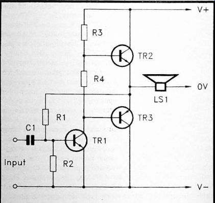
Fig. 2.1 Basic transformerless class B amplifier circuit TR1 is the driver
transistor, and it operates as a straightforward common emitter amplifier
having the series resistance of R3 and R4 as its collector load resistance.
The reason for having this split load resistance will be explained
later. TR2 and TR3 are the complementary output transistors, and these
operate in the emitter follower mode. Unlike the driver stage, they
provide no voltage gain, but they do provide a large amount of current
gain. They therefore act as buffers which enable the high drive currents
required by the loudspeaker to be satisfied.
Biasing of the whole circuit is provided by R1 and R2, which must set the quiescent output voltage accurately at the central 0 volt supply level. With a d.c. coupled circuit this requires the use of a preset resistor to enable the d.c. output potential to be trimmed to precisely the correct level. This is not always necessary with capacitively coupled circuits, where the output coupling capacitor prevents any strong direct current flow if the biasing is not spot-on.
Negative feedback is applied over the circuit via the bias resistors. This reduces the circuit's voltage gain, and also helps to reduce noise and distortion. C1 provides d.c. blocking at the input of the circuit.
On positive output excursions TR3 is cut off, but TR2 is biased into conduction and supplies current to the loudspeaker. On negative output excursions it is TR2 that is cut off, and TR3 that supplies the drive current to the loudspeaker, The higher the output voltage on half cycles of either polarity, the higher the current that is drawn from the appropriate supply rail.
This type of circuit might seem to be unnecessarily complicated, offering no obvious advantage over a simple class A type. However, with a class A output stage there is a constant and very high current consumption. Even if the amplifier would always be run continuously at full power, a class A output stage would not offer a very high level of efficiency.
In fact most of the supply current tends to end up in the output transistor and the load circuit, rather than in the loudspeaker. Class A output stages often offer efficiencies of only about 20% to 25%. Of course, in practice no audio power amplifier is driven continuously at full power by a sinewave input signal, and the true efficiency is likely to be only a few percent.
When driven continuously at full power, class B output stages can provide theoretical efficiencies of around the 70% mark. Practical circuits will often fall well short of the theoretical maximum efficiency level, but will still be far superior to class A designs in this respect. This means that for a given output power they require smaller power supplies, and less heatsinking on the output transistors. They consequently tend to be smaller and cheaper than class A designs, despite what are usually more complex output stages. Unlike class A designs, class B output stages do not consume a high power level when there is little or no output signal. The current consumption is proportional to the output power, and is zero with no input signal. As we shall see shortly, practical designs normally have some quiescent current flow through the output transistors, but this is usually only a small fraction of the quiescent current drain of a class A circuit of similar output power.
Cross-over Distortion
Class B amplifiers might seem to be too good to be true, and as one might expect, there is a catch. This is in the form of crossover distortion. This is a severe type of distortion which is at its worst at low power levels, where distortion tends to be most noticeable. The problem arises because transistors do not start to conduct as soon as a forward bias voltage is applied. For silicon bipolar transistors it is normally necessary for the bias voltage to reach something like 0.5 to 0.6 volts before the device starts to conduct. Thereafter, only a small increase in the bias voltage is needed in order to cause the device to conduct heavily.
If we apply this to our simple class B amplifier circuit of Figure 2.1, it means that the collector of TR1 has to swing about 0.5 to 0.6 volts positive or negative before the output voltage will start to change at all. If we apply this to a triangular output waveform, the correct output waveform is shown in Figure 2.2 (top). The lower waveform is how the output signal might actually appear. This distortion looks bad, and sounds even worse!
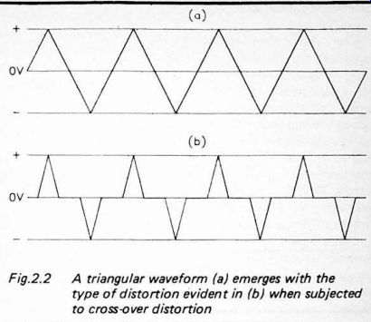
Fig. 2.2
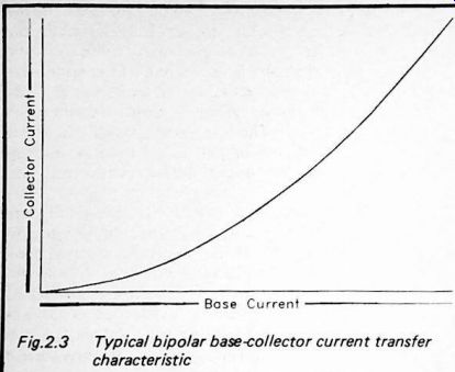
Fig. 2.3
A forward bias is normally applied to the output transistors under quiescent conditions in order to counteract cross-over distortion. This is the purpose of R4. In practice it is not good enough to merely bring the output transistors to the brink of conduction. A bipolar transistor has a relatively low gain as it initially switches on. The gain steadily increases as the collector current is increased, and then flattens out at fairly high currents. It might then actually drop away slightly at very high currents. A typical transfer characteristic might look something like the graph of Figure 2.3 (which is actually exaggerated slightly in order to emphasize the non-linearity of a transistor).
This means that in practice an amplifier based on bipolar transistors, or any other amplifying device available at present come to that, can never offer complete freedom from distortion. The amplifier must be designed to keep the innate distortion level as low as possible, with negative feedback then being used to reduce the actual distortion level of the circuit to an acceptable figure. Negative feedback can reduce distortion levels by substantial amounts, but it is not a total solution. With an innate distortion level, that is (say) 2% or less, negative feedback which produces a 40dB reduction in gain (i.e. reduces the voltage gain by a factor of one hundred) will also reduce the distortion levels by a factor of one hundred. This would give an impressive distortion figure of 0.02% or less. Using a small quiescent bias through the output transistors is not likely to give an innate distortion figure of 2% though. At low signal levels it would probably be around 50% or more! Even with a substantial 40dB of feedback, this would still leave some 0.5% or more distortion.
Thermal Runaway
Using a higher bias current will still leave a reasonably low quiescent current consumption, and will not significantly affect the efficiency of the amplifier. However, it will lead to problems with thermal runaway. The important fact to bear n mind here is that the threshold voltage of a bipolar transistor is temperature dependent. The higher the temperature of the component, the lower its threshold voltage. If the quiescent bias current is set at the correct level while the output transistors are cool, as they heat up in use, the quiescent current will climb. This can result in a regenerative action where the increased heat causes an increase in the bias current, which causes further heating, a further increase in the bias current, and so on. The bias current steadily increases regardless of whether the amplifier is driven, eventually leading to the destruction of the output transistors. This effect is thermal runaway.
With any class B amplifier of this general type and of more than very modest output power, it is essential to take steps to counteract thermal runaway. This is sometimes achieved using a negative temperature coefficient thermistor in the R4 position. This detects any increase in temperature, and its resistance then falls. This results in a reduction in the bias voltage, which stabilizes the bias current. In practice it is difficult to find a thermistor that maintains the bias current reasonably accurately. Only very slight under-compensation is needed in order to let thermal runaway still occur, albeit more slowly than would otherwise be the case. Slight over-compensation will reduce the bias current, giving noticeable cross-over distortion.
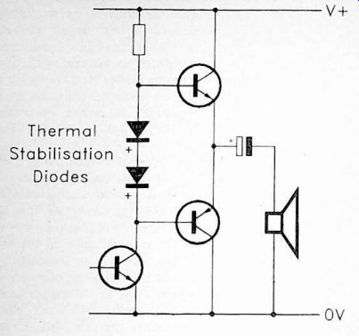
Fig. 2.4 Using two diodes to give a thermally stabilized quiescent bias
current.
The more modern approach is to use two diodes, as in Figure 2.4, or a transistor in the so-called "amplified diode" configuration, as shown in Figure 2.5. The two diodes are forward biased, and act rather like low voltage zener diodes.
About 0.6 volts is needed in order to bring each one into conduction, but only a marginally higher voltage is needed in order to produce a strong current flow. This gives a voltage of about 1.3 volts across the two diodes, which is about right to give a moderate quiescent current flow through the output transistors.
In practice the diodes are mounted very close to the output transistors, and might even be mounted on their heatsink. The diodes therefore quickly respond to any change in the temperature of the output transistors. Like the threshold voltages of the output transistors, the threshold potentials of the diodes are temperature dependent. Increases in temperature cause a reduction in their "zener" voltage, and tend to counteract any increase in the output bias current. Provided the diodes are suitable silicon types, they will have thermal characteristics that are a good match for the output transistors, and which give a stable quiescent current.
The problem with this simple method of stabilization is that there is no certainty that the bias current will be stabilized at a suitable level. Ideally it should be possible to trim the quiescent output current to a suitable figure, which is possible using the amplified diode method of stabilization. This simple configuration gives what is a sort of variable zener diode. If the preset resistor provides half the collector voltage to the base terminal, then it will stabilize the emitter to collector voltage at about double the base voltage. This gives a "zener" voltage of about 1.3 volts, like the two diode circuit. However, by adjusting the preset resistor it is possible to trim the voltage substantially either side of this figure, permitting practically any desired quiescent output current to be set.

Fig.
2.5 Using an amplified diode to provide thermal stabilization of the
bias current.
The "zener" voltage is a factor of the base voltage, and increases in temperature cause the collector and base voltages to drop. This gives the required thermal stabilization of the quiescent bias current, and provided the transistor in the amplified diode circuit is a suitable silicon type, very accurate stabilization will be obtained.
Power MOSFETs
This is all very well in theory, but in practice it can be difficult to obtain really stable bias levels. It is easier when designing amplifiers that will be produced commercially, since there will be no significant physical difference between one amplifier and the next. The same is not true of designs for the home constructor, where there are likely to be a wide variety of cases, heatsinks, etc., used in each amplifier. Rather than all being the same, it would be reasonable to expect no two home constructed projects of the same design to be absolutely identical! Provided each amplifier is carefully constructed, set up, monitored initially, and if necessary readjusted or modified slightly, there should be no problem. This is a less than ideal situation though, and not all constructors will be equipped to handle this task. Ideally what is needed is a circuit that has inherently good thermal stability. This is indeed possible using power MOSFETs in what is essentially the same configuration as Figure 2.1. The only change necessary is to replace the n.p.n. and p.n.p. bipolar transistors with N channel and P channel power MOSFETs respectively.
Like bipolar devices, power MOSFETs require a forward bias before they will start to conduct. Also like bipolar devices, they offer relatively low gains with small forward biases. Accordingly, they also require a fairly strong forward bias when used in a class B power amplifier circuit if strong cross-over distortion is to be avoided. The forward threshold voltage of a power MOSFET is generally somewhat higher than that of a bipolar transistor, and so a somewhat stronger bias voltage is normally needed.
One of the big advantages of power MOSFETs is that they have a positive temperature coefficient at low currents, but a negative type at medium and high currents. If the quiescent current is set at a low level, as the output transistors heat up, the bias current increases slightly. However, it does not increase very much, since the quiescent current soon reaches the turn-over point where the temperature coefficient becomes negative. Further increases in temperature then cause a slight reduction in the quiescent bias current. This changeover from a positive to a negative temperature coefficient tends to stabilize the quiescent current quite close to the current at which the changeover occurs.
In practice the power f.e.t.s that are intended for class B audio power use are designed to have a changeover current which is a good choice for the quiescent bias level (typically about 60 to 100 milliamps). This results in excellent thermal stability without the need for any temperature compensation circuits. In fact the inherent' thermal stability of a power MOSFET output stage means that any attempt to provide a thermal stabilization circuit would probably make matters worse rather than better. For the home constructor the absence of any problems with thermal stability, and getting compensation circuits set up correctly, obviously makes life very much easier. If nothing else, it gives peace of mind as there is no risk whatever of thermal runaway occurring with this type of output stage.
Parallel Operation
There is a potential problem with using bipolar transistors at high powers, and this is secondary breakdown. Basically this means that there are voltage and current combinations which are not acceptable, even though they are within the device's Vceo and Ic ratings, and will not result in excessive power and heat dissipation. Apparently this is due to a sort of localized thermal runaway causing "hot-spots" in the semiconductor structure. The effect of these "hot-spots" is to cause a virtual short circuit from the collector to the emitter, resulting in the rapid destruction of the device. Due to their negative temperature coefficient at high operating currents, power MOSFETs do not suffer from secondary breakdown. Whereas bipolar power transistors often have to be used well within their maximum voltage and current ratings in order to operate reliably, power MOSFETs can be used right up to both ratings without any risk of them being damaged (provided the power ratings are not exceeded of course).
A practical benefit of this absence of secondary breakdown is that it is possible to use power MOSFETs safely in parallel.
In other words, each output transistor can actually consist of two devices connected in the manner shown in Figure 2.6.
This shares the current between the two transistors in each parallel pair, permitting higher output currents and powers to be handled. In fact by using this arrangement it is possible to halve the loudspeaker impedance, and double the output power.
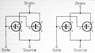
Fig. 2.6 Power MOSFETs can be used safety with this straightforward parallel
connection.
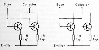
Fig. 2.7 Emitter resistors are needed when using bipolar transistors
in parallel.
This is actually a slight over-simplification, and for this method to be fully successful it is necessary to have a driver circuit that can take the additional loading of the extra output transistors. This is not difficult with power MOSFETs, since they have the high input impedances associated with all f.e.t. devices. The input capacitance of power MOSFETs precludes the use of true micro-power driver stages, which would give an inadequate high frequency response due to the capacitive loading of the output stage. A driver current of only about 10 milliamps is normally adequate though.
The very low drive currents required by power MOSFETs gives them a major advantage over bipolar transistors. In order to obtain comparable gain at least two bipolar transistors have to be used. The Darlington pair configuration is probably the more popular configuration, but the twin common emitter type with 100% negative feedback is also used to a significant degree. Both configurations effectively provide a single transistor having a current gain equal to the products of the two gains of the individual transistors in the pair. For instance, if the current gains of the two transistors in a pair are 50 and 60, they effectively provide a single transistor having a current gain of 3000 (50 x 60 = 3000). Even so, quite high drive currents of a few hundred milliamps are often needed in very high power circuits. Bear in mind here that in order to work efficiently, the amplifier must have an output impedance that is only a small fraction of the loudspeaker impedance. A typical medium or high power audio amplifier has an output impedance of a few milliohms or less.
With power MOSFETs the parallel arrangement is inherently stable. If one device tends to draw more current than the other, it heats up more, but the negative temperature coefficient results in it taking a lower proportion of the current. In other words, the characteristics of power MOSFETs results in them tending to stabilize with an almost identical share of the output current.
The situation is very different with bipolar transistors when they are used in a similar arrangement. If one device takes more current than the other, it heats up more, which due to its positive temperature coefficient results in it taking a greater proportion of the output current. This results in it heating up still further, taking an even greater share of the output current. The other device takes an ever decreasing proportion of the output current, which results in it operating cooler. This in turn causes it to take a lower proportion of the output current. Rather than tending to stabilize with an even share of the output current, the tendency is for one device to take an ever increasing share of the output current, while the other takes less and less. This is quite likely to ultimately result in the destruction of the output transistor that takes the "lion's share" of the output current.
The normal way around this problem is to use emitter resistors, as in Figure 2.7. Output currents (low through these resistors, causing voltages to be produced across them.
These voltages effectively raise the base to emitter voltage needed for a given collector current. The higher this current, the higher the required base to emitter voltage becomes. If one transistor takes a higher share of the current flow, this results in its effective base to emitter threshold voltage increasing. At the same time, the other device takes a lower current, and its effective base to emitter turn on potential reduces. This tends to reduce the current through the device that takes the higher current, and increase the How through the transistor that takes the lower current. In other words, it tends to even out any discrepancies in the two current flows. Provided the resistors are high enough in value, and the gains of the transistors are not too dissimilar, this will ensure stable operation of the circuit. Incidentally, these emitter resistors are sometimes included when single output transistors are used. It helps to guard against thermal runaway.
In practice it is undesirable to include these resistors because they produce voltage drops. These voltage drops are reflected in a reduction in the output voltage swing. In practice this is the price that has to be paid in order to obtain reliable operation. In fairness, it has to be admitted that the "on" resistances of power MOSFETs tend to be higher than the equivalent figures for bipolar transistors. Thus, even with these resistors added, pairs of bipolar transistors might actually provide lower "on" resistances than pairs of power MOSFETs. Note that if bipolar transistors are used in parallel pairs, it is normal for each pair to be mounted on the same heatsink. This gives a thermal coupling between the two devices, which helps to discourage any creeping apart of their relative shares of the output current.
Although we have only been talking here in terms of pairs of transistors connected in parallel, it is possible to use any desired number of transistors in parallel. In practice though, there may be no point in doing so. The more transistors that are connected in parallel, the greater the drive current that is needed. This could lead to an impractical collector current being needed in the driver stage. Probably the main point to bear in mind is that this method only permits higher output currents to be obtained -- not higher output voltages.
It is possible that the parallel transistors would produce lower voltage drops, and would give slightly boosted output voltage swings. This would be more likely to occur with power MOSFETs than bipolar transistors, since the voltage drops across single power MOSFETs are often quite high. This is due to their relatively high "on" resistances. However, this effect is not likely to produce a boost in output power of more than a few percent.
The doubling in the output current, provided the power supply has a suitably high current rating to give this increased current, gives a doubling of output power. This is only obtained by halving the load impedance though. In practice there will be a limit on minimum load impedance that can be used.
This often precludes the use of more than two devices in parallel, but it is worthwhile remembering that more devices can be used if necessary.
Speed
In the early days of power transistors there was a major problem in getting the devices to operate at speeds that would enable them to be used in practical applications. For high frequency operation it is necessary to make transistors physically small, but in order to permit high powers to be handled they must be physically large (or relatively so anyway). This makes it difficult to obtain both high power and high operating speed. Most of the early power transistors were barely usable in low quality audio applications, and only a few "specials" were capable of operating at radio frequencies.
Most of these radio frequency devices would only operate up to a few mega-hertz.
Matters improved when silicon transistors took over and the original germanium devices became obsolete. Even so, many high power bipolar transistors have low Fr ratings, and are prone to problems with slewing induced distortion (or SID as it is often termed). This is where a strong high frequency signal requires the output voltage to change at a high rate which is beyond the capabilities of the output transistors.
These signal conditions may only occur infrequently, but the resultant distortion can be quite severe, and very noticeable indeed.
The high frequency performance of good quality power devices designed specifically for operation in audio power amplifiers is usually much better than that of general purpose high power devices such as the ever popular 2N3055. The cost is generally somewhat more, but the difference is not usually large enough to greatly affect the overall cost of the finished amplifier complete with power supply. Most of the cost is usually accounted for by the mains transformer, massive heatsinks, the case, etc., rather than the semiconductors. Where really high output powers are required, there may be no option but to resort to very high power devices having quite low F, figures (usually only about 200kHz). Although a figure of about 200kHz might seem perfectly adequate for the 20 kHz audio bandwidth, remember that this is not the frequency at which the gain starts to fall away. It is the frequency at which the gain falls to unity, which really means it is the frequency at which the device ceases to offer any worthwhile gain at all! Of course, in many high power audio applications the audio quality might be of secondary importance to the output power, and something short of true hi-fi performance may be quite acceptable. In particular, if the amplifier will only be required to handle voice signals, slewing induced distortion is not likely to be a significant consideration. Any slewing induced distortion that should occur will not matter very much, and the nature of the input signal is such that there is little likelihood of this type of distortion occurring anyway.
A factor that could still cause problems is the significant phase lag that occurs through a relatively slow output stage.
This results in feedback that should be of the negative variety being inverted and converted into positive feedback. In a minor case this could result in "ringing" and other relatively mild forms of high frequency instability. In a severe case it results in the circuit breaking into oscillation usually at an ultrasonic frequency. This problem is avoided in practice by using so-called "compensation" components, which can be anything from a single low value capacitor through to several C-R circuits. With a very slow output stage the high frequency response of the circuit might have to be rolled-off at quite a low frequency, possibly severely attenuating the higher audio frequencies. Again, this will not matter if the amplifier is only required to handle voice signals, but it would clearly be a major drawback where music signals are involved.
Slewing induced distortion is less of a problem if power MOSFETs are used in the output stage. These have relatively high operating speeds, and are typically some fifty to one hundred times faster than silicon power transistors having similar power ratings. This is normally sufficient to totally eliminate any problems with slewing induced distortion, or inadequate bandwidth due to the use of heavy frequency compensation. In fact power MOSFET based amplifiers will often operate with good stability even if no frequency compensation circuit is used. In practice it is normal for such a circuit to be included. This is done in order to avoid problems such as the breakthrough of radio frequency signals picked up in the input wiring.
Most audio power amplifiers use configurations that are more complicated than the one of Figure 2.1. This configuration is simple, but it has a number of flaws. One of these is that it does not have a very high innate (open loop) voltage gain, leaving little scope for reducing distortion by using large amounts of negative feedback. It does not have a particularly low innate distortion level either. Practical circuits normally have two common emitter stages ahead of the output stage in order to boost the open loop voltage gain to a more useful level. In order to reduce the distortion of the driver stage it is often equipped with a constant current source as its collector load, in place of a simple resistor. For the same reason, the input stage is often a "long tailed pair" rather than a simple common emitter stage. We will deal with some of these improved configurations in the next Section, which covers some practical amplifier circuits plus suitable mains power supply units.