So far we have only talked in fairly broad and rather theoretical terms. In this Section some practical high power audio amplifier circuits will be described, complete with suitable printed circuit board designs in some cases. Although these circuits can probably be constructed by anyone who has a certain amount of experience at electronic project construction, I must emphasize that I do not consider these designs to be suitable for those of limited experience at this type of thing. High power audio amplifiers tend to be very unforgiving it mistakes are made, and even those who have many years of experience at project construction need to proceed carefully with these (or any other) high power audio circuits.
Configuration
The basic class A driver and class B output stage described in Section 2 will work in practice, but will not give particularly good results. The open loop voltage gain of this simple arrangement is quite low, giving little scope for the application of negative feedback in order to improve performance. An extra stage of amplification is needed in order to overcome this problem, and give better results. Figure 3.1 shows what is generally considered to be the most simple configuration that is capable of providing reasonably good results. This is shown as having a pair of power MOSFETs in the class B output stage, but this configuration can obviously be used with a complementary bipolar output stage if preferred.
The driver and output stages are much the same as in the basic configuration described in Section 2. The difference is in the addition of a common emitter stage (TR1) at the input of the circuit. This has its output direct coupled to the input of the driver stage, making the entire circuit direct coupled (apart from the d.c. blocking capacitors at the input and output, of course). Although a common emitter amplifier would normally be expected to provide a very high level of voltage gain (typically about 50dB for a high gain silicon device), the overall voltage gain of this circuit is just unity.
This is due to the 100% negative feedback from the output to the emitter of TR1, via R6. R1, R2 and R3 are used to bias the input of the circuit to about half the supply voltage, which in turn gives the required output bias level of half the supply potential. R1 and C2 act as a so-called "hum" filter, which prevent any mains "hum" or other noise on the supply lines from being coupled to the input of the amplifier via the biasing network.
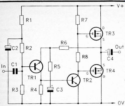
Fig. 3.1 The most simple power amplifier configuration that will provide
reasonably good results
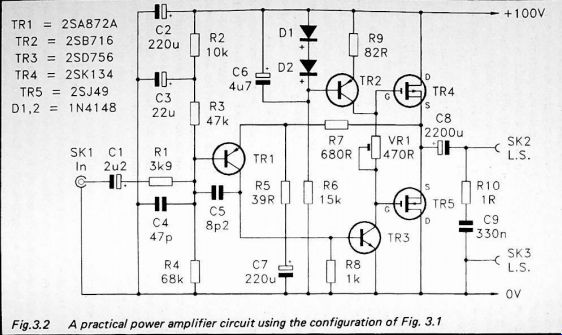
Fig.3.2
In order to give the circuit a useful voltage gain at audio frequencies it is necessary to remove some of the negative feedback at these frequencies. The feedback must not be altered at d.c., since this would upset the biasing conditions.
C3 decouples the feedback at audio frequencies, but provides d.c. blocking that leaves the biasing unaltered. R5 limits the amount of feedback that is removed, and therefore controls the closed loop voltage gain of the circuit. This operates in a similar manner to an operational amplifier used in the noninverting mode, and the voltage gain is equal to (R5 + R6) divided by R5. The open loop gain of the circuit is likely to be quite high at (typically) about 70dB. This means that the circuit can have a useful closed loop gain of around 30dB while still having about 40dB of feedback to reduce the distortion to an acceptable level.
Practical Circuit
The circuit diagram of Figure 3.2 is for a practical power amplifier based on the configuration of Figure 3.1. This follows the original configuration quite closely, but it has a few refinements. At the input of the circuit, R1 and C4 provide a simple lowpass filter action. This removes any high frequency signals that might be present on the input signal, and which could otherwise cause unwanted audio breakthrough or other problems. C5 provides a small amount of high frequency roll-off which helps to avoid problems with high frequency instability. R10 and C9 are included for the same reason, and they are needed to compensate for the highly inductive nature of a loudspeaker, which represents an awkward load.
In the driver stage the simple load resistor for TR3 has been replaced with a constant current generator based on TR2. A constant current load has certain advantages, such as improved linearity from the driver stage. The constant current source sets the operating current of the driver stage at only about 8 milliamps, but this is adequate for the power MOSFET output stage. VRI enables the quiescent output current to be adjusted, and in practice it should be adjusted for a bias level of about 80 milliamps. The specified values for R7 and R5 give a closed loop voltage gain of a little under 26dB. This means that about 4 volts peak to peak is needed at the input in order to fully drive the amplifier. If necessary, the gain can be boosted somewhat by making R7 higher in value (increases in its value giving a proportionate boost in gain). This will result in a slight increase in the noise and distortion figures though.
Although this amplifier is very simple, it provides quite good performance. I would not claim true hi-fi performance from it, but I suppose it is true to say that it betters many amplifiers which have claimed this status. Provided it is not driven into clipping, the distortion level should be only a fraction of 1% at any power level. This includes very low powers where many otherwise excellent amplifiers give disappointing results. It has an open loop voltage gain (and therefore a feedback level) which is virtually constant over the audio range, resulting in a distortion performance which is much the same over the full audio spectrum. The same is not true of many power amplifiers which have bipolar output transistors, where there is often a marked loss of performance at high audio frequencies.
The unweighted signal to noise ratio should be better than 80-dB, assuming that the "hum" content is minimal. The value of C3 can be increased to give better "hum" filtering at the input. if this should prove to be necessary. Pick-up of "hum" in the input wiring is a more likely cause of problems, and this can be avoided by using a good quality screened lead to make the connections between the circuit board and SK1.
The maximum output power depends on the load impedance and the supply voltage used. I would recommend that the unloaded supply voltage should not exceed about 100 volts. In the components list the maximum operating voltages of the electrolytic capacitors are given on the basis that the supply voltage will never exceed this figure. Apart from this factor, the maximum collector - emitter voltage ratings of the transistors must be taken into account. All three bipolar devices have a rating of 120 volts (the output devices have a maximum drain-to-source voltage rating of 140 volts incidentally).
Output Power
With the specified supply potential of 100 volts, and an 8 ohm loudspeaker, the circuit should comfortably achieve an output power of more than 50 watts r.m.s. Note that we are talking here in terms of a genuinely continuous r.m.s. rating, and not some form of transient power rating. We are also talking here in terms of the output power below the point at which there is any hint of clipping. Where very low distortion is not needed, the circuit can be pushed to somewhat higher power levels. Adjusting the value of R3 to give symmetrical clipping (with a loaded output) can also help to optimize the power performance, although it might not make much difference to the perceived volume level provided by the amplifier. With the biasing optimized, and the amplifier driven to the point where the distortion level is a few percent, the output power should be somewhere in the region of 75 watts RMS Again, we are talking here in terms of a true continuous RMS level.
This amplifier's output power is somewhat less than one might expect, given that the supply potential is about 100 volts and the load impedance is 8 ohms. It would seem to be reasonable to expect an output voltage swing of about 80 volts or more, which equates with an r.m.s. output power of over 100 watts. However, as explained previously, the "on" resistance of a power MOSFET is rather high by the standards of high power semiconductors, and this results in voltage drops that significantly reduce the maximum output voltage swing.
It should also be borne in mind that 100 volts is the unloaded supply voltage, and that it will "sag" slightly when fully loaded.
In order to obtain higher output powers the power supply can have a mains transformer with a higher current rating than the minimum requirement, so as to minimize the loading of the supply voltage at high output powers. Another method is to use pairs of parallel connected power MOSFETs in the output stage. This reduces the voltage drops through the output stage, and boosts the output voltage swing quite significantly. If both these methods are adopted, the circuit should be able to manage at least 80 watts r.m.s. without too much difficulty, and will probably be able to exceed 100 watts RMS before the onset of severe clipping and serious distortion.
Taking things one step further, the load impedance can be reduced to 4 ohms. In conjunction with parallel pairs in the output stage, and a suitably hefty mains transformer in the power supply, this should permit output powers of over 150 watts RMS to be achieved. I have not extensively tested the amplifier under these conditions, but some quick checks would suggest that an output power of around 160 watts at reasonably low distortion is quite achievable. Although you might think that halving the load impedance would double the maximum output power from around 100 watts r.m.s. to about 200 watts r.m.s., matters are not quite as simple as this.
Reducing the load impedance increases the voltage drops through the output stage, and prevents this simple doubling up of the output power. Using further output transistors in parallel with the existing ones will rectify this problem.
Note though, that using several parallel connected devices for each output transistor gives an increase in the input capacitance of the output stage, which effectively rolls-off the high frequency gain of the driver stage. This is reflected in a degradation of the distortion performance at high frequencies.
However, this problem is not likely to result in a serious loss of performance, and is a perfectly practical approach if it is important to squeeze as much power out of the unit as possible. By doing this it should be possible to obtain about 200 watts r.m.s. into a 4-ohm impedance load, but I must stress that I have not tried this in practice, and can not guarantee that it will give the desired result.
Power Supply
A suitable mains power supply circuit for the MOSFET power amplifier is shown in Figure 3.3. This is an entirely conventional circuit using a fullwave bridge rectifier. It is assumed that the mains plug will be fitted with a 2-amp or 3-amp fuse. If not, then a 2-amp fuse should be included in the power supply circuit in series with SI a. Do not omit the 3-amp fuse at the output of the supply, as this is the only overload protection for the circuit. You might care to add a 3-amp fuse in one of the secondary leads of T1. This would give protection against a fault in C1 or the bridge rectifier.
Note though, that this fuse would have to be of the anti-surge type, and not of the more usual "quick-blow" variety. A "quick-blow" fuse would almost certainly live up to its name at switch-on, due to the high surge current as C1 took up its initial charge.
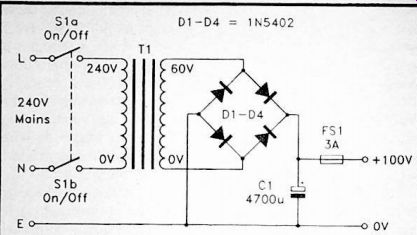
Fig.3.3 The mains power supply circuit.
The minimum suitable current rating tor T1 depends on the way in which the power amplifier is used. Two amps should be adequate if the unit is used with an 8-ohm impedance loudspeaker, even if it is likely to be driven fairly heavily. A rating of 3 amps is preferable if the unit will be used with parallel pairs in the output stage and driven heavily. If parallel pairs in the output stage plus a 4-ohm load impedance are used, then a rating of 4 amps or more would be necessary. With multiple output transistors and a 4-ohm load, a current rating of around 5 amps would be preferable. It would also be necessary to use a 5-amp fuse for FS1, and C1 would preferably be increased to 10000uF in value (or two 4700 uF capacitors connected in parallel could be used). D1 to D4 have a rating of 3 amps, and would need to be replaced with components having ratings of at least 200 volts and 5 amps. Although the bridge rectifier is shown as being made up from four individual rectifiers, it is perfectly acceptable to use a ready-made bridge rectifier assembly having suitable voltage and current ratings.
For stereo operation I would recommend having separate power supplies for the two amplifiers. SI would, of course, be common to both supplies, and the mains transformer could be a type having twin secondaries, one for each supply circuit.
The other components would have to be duplicated in the two supply circuits.
Construction
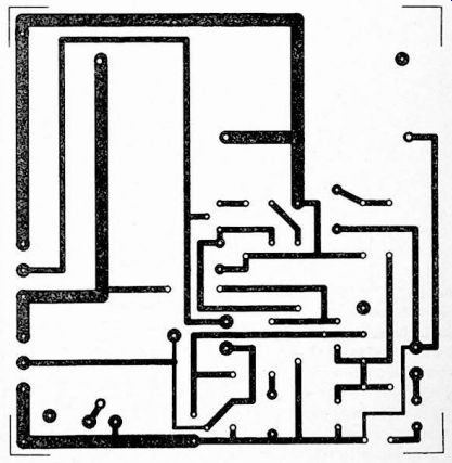
Fig. 3.4 The copper track pattern for the MOSFET power amplifier
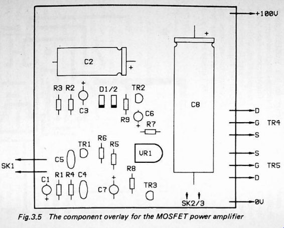
Fig. 3.5
A suitable printed circuit design for the MOSFET power amplifier is shown in Figure 3.4 (copper track pattern) and Figure 3.5 (component overlay). Construction of the board follows the usual lines and should not present any difficulties.
There are several points which must be kept in mind when dealing with the overall construction of the amplifier though.
R10 and C9 are not fitted on the board, but are connected across the loudspeaker sockets (SK2 and SK3). where they should be most effective. SK2 and SK3 should be a type of socket suitable for heavy duty applications. Terminal posts and heavy duty spring terminals are good choices for applications of this type. The supply wiring and the leads to SK2 and SK3 should be completed using a heavy duty connecting wire capable of carrying high currents with minimal losses.
TR4 and TR5 are mounted off-board on suitable heatsinks.
Power MOSFETs. being a form of MOSFET, have very high input impedances. However, the usual anti-static precautions would seem to be unnecessary when using these components.
The main risk of damage is due to unwanted high frequency oscillation, caused by the very high gain of these devices, even at quite high frequencies. The manufacturer recommends that the leads to these devices (especially the leads to the gate terminals) should be no more than 50 millimeters long. If it is essential to use longer leads, then it is recommended that a resistor of about 100 ohms or so in value is connected in series with each gate terminal, and that the resistor should be mounted close to the gate terminal. This is presumably the power MOSFET equivalent to the "base-stopper" resistors that are sometimes used to prevent instability in bipolar based circuits.
Heatsink
Judging the correct rating for a heatsink tends to be a difficult task due to the unknown and variable factors. In theory it is a straightforward task. Heatsink ratings are in degrees Centigrade per watt, and this is their thermal resistance. This is just a measure of the rise in temperature that results from each watt of power that the heatsink receives. For example, with a heatsink having a rating of 2.5 degrees Centigrade per watt, and receiving a power of 4 watts, there will be a temperature rise of 10 degrees Centigrade (2.5 degrees x 4 watts = 10 degrees).
Unfortunately, things are not quite as straightforward as simply taking the power dissipated by a transistor, and multiplying this by the rating of the heatsink in order to get the rise in temperature that will result. There is the thermal resistance of the transistor itself to take into account. Power transistors are designed to provide an efficient transfer of heat from the semiconductor chip to the case, but there is always a significant thermal resistance here. Also, there will be a certain amount of thermal resistance between the case of the transistor and heatsink. This should be relatively minor though, and some silicone grease (or a synthetic substitute) can be used to ensure a good flow of heat from one to the other. When calculating the temperature rise for a given dissipation figure, the thermal resistance used is the sum of these three resistances (i.e. the transistor's rating, the heatsink's rating, and the resistance between the two).
In order to calculate the heatsink rating, you must first decide on the maximum acceptable temperature for the transistor. Next the highest ambient temperature under which the device will operate must be decided. Deducting the ambient temperature from the maximum permissible temperature then gives the maximum acceptable temperature rise.
Dividing this by the power dissipation then gives the minimum acceptable overall thermal resistance. Deducting the transistor's thermal resistance from this, and also deducting the transistor-to-heatsink thermal resistance, then gives the smallest heatsink rating that will give safe operation. Note that with heatsink ratings the higher the figure, the less efficient the heatsink. In other words, one having a rating of (say) 1 degree Centigrade per watt is actually a larger and (or) more efficient heatsink than one having a rating of 3 degrees Centigrade per watt. One having a rating of 1 degree Centigrade per watt is acceptable where a 1.5 degree per watt type is specified, but a 1.5 degree per watt type would not be an acceptable substitute for a 1 degree per watt heatsink.
If we take a simple example of calculating a heatsink rating, assume that a power device must operate under the following conditions:
30°C Maximum ambient temperature
Maximum operating temperature
Maximum power dissipation
Transistor's thermal resistance
Transistor-to-heatsink resistance
180°C
50 watts
2°C per watt
0.5°C per watt
The maximum acceptable temperature rise is clearly 150 degrees (180 degrees - 30 degrees = 150 degrees). With a maximum dissipation of 50 watts, this gives an overall thermal resistance rating of 3 degrees Centigrade per watt (150 degrees divided by 50 watts = 3 degrees per watt). Deducting from this the thermal resistance rating of the transistor (2 degrees per watt) and the transistor-to-heatsink thermal resistance (0.5 degrees per watt) gives a rating of 0.5 degrees Centigrade per watt for the heatsink.
In practice there are a number of problems. Provided full data sheets for the power transistor can be obtained, the thermal resistance rating for the components can be ascertained (this rating is not normally to be found in short-form data). Where the thermal resistance is not quoted, it is sometimes possible to work it out anyway. For power transistors the power ("P_tot") rating is usually one that assumes the transistor is mounted on a notional infinite heatsink, and is at a certain ambient temperature. Assume that the ambient temperature is the usual 25 degrees Centigrade, the transistor has a maximum operating temperature of 175 degrees Centigrade, and its power rating is 100 watts. It can take a maximum temperature rise of 150 degrees Centigrade (175 - 25 = 150), and this is produced with a power of 100 watts.
The thermal resistance is therefore 1.5 degrees per watt (150 divided by 100 = 1.5).
The other figures can be difficult to define accurately. The maximum ambient temperature is something of an unknown quantity, and it is necessary to assume a fairly high figure to allow for the fact that the equipment might be used on an exceptionally hot day, or conditions that for some reason give a high ambient temperature. Also bear in mind that if the heatsink is mounted inside the case, this will result in a large rise in the temperature inside the case. This method of construction is only acceptable if the case is a type which has plenty of large ventilation holes, or large ventilation grilles.
Even so, the temperature inside the case will rise quite significantly, effectively increasing the ambient temperature, would strongly recommend mounting the power transistors and heatsinks on the exterior of the case (normally they are mounted on the rear panel). An alternative is to use a well ventilated case fitted with a cooling fan.
For the maximum temperature you could simply take the maximum temperature rating of the transistor, but this is not a good idea. Although the transistor can operate at this temperature, its reliability is unlikely to be very good at such a high temperature. Also, it leaves no safety margin if the operating conditions should ever be less favorable than expected. It is wise, where feasible, to keep the maximum designed operating temperature substantially below the maximum permissible temperature of the power transistor.
Although you might think that the maximum dissipation in the transistor is something that could be easily calculated, this is not really the case. A worse case figure can actually be calculated quite accurately for a purely resistive load, but a loudspeaker offers a load impedance that varies considerably over the audio frequency range. This renders any power dissipation calculations slightly less than accurate when a "real" load is connected to the amplifier. A reasonable safety margin therefore has to be allowed for. The thermal resistance between the heatsink and the power transistor is an unknown quantity, but it would be reasonable to assume quite a low figure here.
Obviously suitable heatsink ratings can be calculated, allowing generous safety margins where appropriate, but my advice is not to bother with this when dealing with high power audio amplifiers. Simply fit the power devices onto a very large heatsink that should be more than adequate, even if the amplifier is used under awkward conditions. I would strongly recommend the use of considerable overkill in the heatsink rating when using bipolar output transistors, where the threat of thermal runaway is an ever present one. A heatsink having a rating of about 1.2 degrees Centigrade per watt or better for each pair of output transistors should ensure safe and reliable operation with any of the amplifiers featured in this guide.
However, if possible use an even larger type, such as one having a rating of 1 degree Centigrade per watt or less.
Ready-made heatsinks of suitable ratings are available, and some are ready drilled to take two TO-3 power transistors such as the 2SJ49 and 2SK134. Where an amplifier has four output devices, two of these heatsinks are required. Apart from any thermal considerations, it is not physically possible to mount four TO-3 cased transistors on most heatsinks. Alternatively, all four transistors could be mounted on a single heatsink having a rating of about 0.5 degrees Centigrade per watt or less. If you build a bridge amplifier having eight output devices, then you will need either four heatsinks rated at 1.2 degrees Centigrade per watt, or two rated at 0.5 degrees Centigrade per watt (and a large case to accommodate them all!).
Insulation
An essential point to keep in mind is that the metal TO-3 style cases of the power MOSFETs connect internally to the source terminals. As the two source terminals of each complementary pair are connected together anyway, this connection via the heatsink is of no consequence. However, the heatsink will then be connected to the sources of the output transistors, and must not be allowed to come into electrical contact with any other part of the circuit. Normally the heatsink would be mounted direct onto the metal case of the amplifier, which would in turn be earthed to the 0 volt supply rail. Either the output transistors should be insulated from the heatsink using standard TO-3 insulating sets, or the heatsink must be mounted in a fashion that keeps it insulated from the case.
At the very least I would recommend that the output transistors should be insulated from the heatsink. Ideally the heatsink should also be insulated from the case. Any breakdown in the insulation that results in the sources of the output transistors being connected to the earth rail could have dire results. This would place a short circuit on the output of the amplifier, without any d.c. blocking as the output coupling capacitor would be bypassed. The result of this would be a massive current How until the fuse in the power supply cut off the supply. Doubling up the insulation gives good protection against this possibility.
A TO-3 insulating set consists of a thin mica or plastic washer plus a couple of small plastic bushes. The washer fits between the transistor and the heatsink. If the heatsink is not ready-drilled for TO-3 transistors, one of these insulating washers can be used as a template to aid the correct positioning of the mounting holes. It is important that the rims of the mounting holes are free from any protruding pieces of metal, which would almost certainly cut straight through the washer and prevent it from providing the required insulation. If necessary, use a large drill bit to clean up the holes. The two plastic bushes fit over the mounting bolts, and prevent these from providing an electrical connection between the heatsink and the transistor. One final point worth mentioning is that most heatsinks operate at maximum efficiency if they are mounted with their fins in a vertical position (not with them horizontally).
Supply Construction
The electrolytic capacitor in the power supply has a very high value, together with a fairly high voltage rating, which means that it is almost certain to be a single-ended type having tags. These are intended to be mounted on a case or chassis using a simple mounting clip. These clips are available from some of the larger component retailers, but it is not difficult to improvise a suitable clip built from thin sheet aluminum.
It is probably not worth going to the trouble of building the supply on a circuit board of any kind, although you might be forced to do so if the smoothing capacitor is an axial type.
In most cases the supply can be built using simple point-to- point wiring. Figure 3.6 gives details of the supply wiring.
This is quite straightforward, but due care should be taken when constructing the power supply unit. Apart from the fact that the dangerous mains wiring is involved, the voltages and currents on the output side of the supply are also quite high. It is questionable as to whether or not 100 volts could give a serious shock, especially as we are talking here in terms of a d.c. supply rather than an a.c. type (which are generally accepted as being more dangerous). You can certainly get a minor shock from a 100-volt d.c. supply though. Perhaps of greater importance, the current available from the supply is extremely large under overload conditions. Mistakes will almost certainly result in some smoke and one or more of the components in the power supply being destroyed. Be very careful to get the wiring right, and to avoid accidental short circuits. Be especially careful to connect the supply to the amplifier with the correct polarity. This may seem to be a trivial point, but a lot of people have made this mistake and inflicted a lot of expensive damage on their projects! It is assumed in Figure 3.6 that the bridge rectifier is made up from four separate rectifiers. The leadouts of the rectifiers should be left fairly long (which they will probably have to be anyway), as they act like heatsinks, and help to remove heat from these components. If a ready-made bridge rectifier assembly is used, this should have " + " and " - " signs to show the two output leads and their polarity. The two leads which connect to the secondary winding of T1 will probably be marked with " ~ " symbols. With most bridge rectifiers that are designed to handle up to a few amps they must be mounted on a heatsink. The case or chassis should be more than adequate as the heatsink.
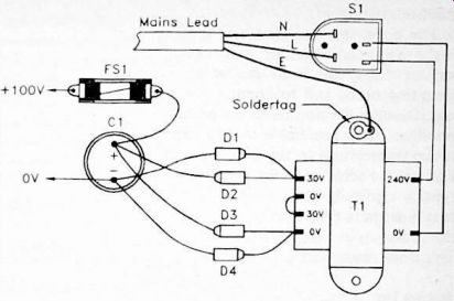
Figure 3.6
It is also assumed in Figure 3.6 that the mains transformer has twin 30-volt secondary windings connected in series to give the required 60-volt a.c. output. A twin 30-volt type is likely to prove somewhat easier to obtain than a 60-volt type, but the latter can obviously be used if you can track down a suitable component.
The metal case and chassis of the amplifier must be earthed to the mains earth lead for safety reasons. Probably the easiest way of doing this is to mount a solder-tag on one of T1's mounting bolts, and to connect the mains earth lead to this tag. Observe the normal safety precautions when building the amplifier. It is preferable for the exposed mains wiring, such as the connections to the on/off switch (S1), to be insulated.
This can be achieved using p.v.c. sleeving, and the heat-shrink type is especially good for this type of thing. Note that the case must be a type having a lid or cover secured by screws so that there is no easy way for anyone to gain access to the dangerous mains wiring.
Setting Up
Before switching on the amplifier, make sure that VR1 is adjusted in a fully counter-clockwise direction so that it inserts minimum resistance into the circuit. Where possible, I would recommend trying the amplifier first with a bench power supply. It can then be operated at a reduced supply voltage for initial checking purposes. Somewhere in the region of 20 to 30 volts should be sufficient to operate the circuit properly to give a reasonable output power for testing purposes. The power supply should have current limiting that will protect the components in the amplifier in the event that a mistake has been made, or a component is faulty. If a suitable power supply unit is not available, power the unit from its mains power supply unit via a resistor of about 47 ohms in value and having a power rating of about 10 watts. This will provide some protection if the amplifier is faulty in some way, but it should permit it to operate at low power so that you can ascertain whether or not it is functioning properly.
If there is any sign of a malfunction, other than reduced output power due to the supply restrictions of course, switch off at once and recheck the amplifier wiring, etc. If all is well, connect the unit to the mains supply unit, with no current limiting resistor being included. It should then work quite well, providing plenty of output power, but the distortion performance at low volume levels will probably not be very good. Use a multimeter set to a high d.c. current range to measure the current consumption of the unit. Temporarily removing FS1 in the power supply unit and connecting the multimeter across the fuse holder is an easy way of arranging things. With no input applied to the amplifier the current consumption should be something in the region of 10 milliamps. Adjusting VR1 in a clockwise direction should cause a steady increase in the current consumption. Advance VR1 to the point where the current reading reaches about 90 milli- amps. With the multimeter removed and the fuse restored to its holder, the amplifier is ready for use.
Components
Amplifier (Fig.3.2)
Resistors (all 0.25 watt 5% carbon film)
R1 3k9 R2 10k R3 47k R4 68k R5 39 R R6 15k 680 R R7 R8 1-k R9 82R R10 1R
Potentiometer
VR1 470R sub-min hor preset
Capacitors
2p2 100V radial elect 220m 100V axial elect 22m 100V radial elect 47p ceramic plate 8p2 ceramic plate 4m7 63V radial elect 220m 100V radial elect 2200m 100V axial elect 330n 100V polyester
C1 C2 C3 C4 C5 C6 C7 C8 C9
Semiconductors
TR1 TR2 TR3 2SA872A 2SB716 2SD756 2SK134 2SJ49 1N4148 1N4148 TR4 TR5 D1 D2
Miscellaneous
SKI SK2
Standard jack, or phono, etc.
Terminal post or spring terminal
Terminal post or spring terminal
Large (1.2 degrees Centigrade per watt or better) heatsink Two TO-3 insulating kits
Printed circuit board Wire, solder, etc.
SK3
Note that, as explained in the main text, some supply voltage and load combinations require the use of two 2SK134s in parallel for TR4, and two 2SJ49s in parallel for TR5. The 2SA872 has a lower V,
as opposed to 120 volts), but it should just about be adequate in this design. The 2SA872A gives a greater safety margin, and is the better choice though. A 2SB646A is suitable for TR2, and a 2SD666A is suitable for TR3.
rating than the 2SA872A (90 volts ceo Power Supply (Fig. 3.3) SI Rotary mains switch
Mains primary, 60 volt secondary (refer to text for details of the required current
ratings) 1N5402 1N5402 1N5402 1N5402
4700/j 100V single ended electrolytic with tag connections
T1 D1 D2 D3 D4 C1
FS1 3A (or 3.15A) 20mm quick-blow 20mm chassis mounting fuse holder
Mounting clip for C1
Wire, solder, etc.
Please read the notes in the main text regarding the power supply components before ordering the power supply components.
Op Amp Techniques
Operational amplifier techniques, with a d.c. coupled output, are often used in high power audio amplifier designs. One advantage of this method is that it avoids the need for a large (and expensive) output coupling capacitor. It can also bring advantages in terms of performance (particularly distortion at low signal levels), and makes it relatively easy to produce reliable bridge amplifier designs.
Figure 3.7 shows the basic configuration used in a power amplifier of this type. The output stage is of the usual class B complementary variety. The driver stage is a "long tailed" pair, with another long tailed pair being used as the input stage. D.C. coupling is used throughout, with the usual (tor operational amplifier type circuits) dual balanced power supplies. The circuit is shown here as a non-inverting amplifier. R1 biases the input to the 0-volt supply potential, while R10 and R5 form the negative feedback loop. The input impedance of the circuit is equal to the value of R1, although with a basic operational amplifier circuit this is dependent on the value of R1 not being very high in value.
The input impedance of the amplifier itself can then be ignored. The closed loop voltage gain of the circuit is equal to (R10 + R5) divided by R5.
As we shall see later, this type of circuit is easily reconfigured to operate as an inverting amplifier. This makes it easy to provide a bridge amplifier action. You simply require an inverting amplifier and a non-inverting type, with the two having feedback circuits which provide accurately matched voltage gains. With the input signal connected to the inputs of both amplifiers, and the loudspeaker connected across the non-earth outputs of the amplifiers, this gives a very good bridge amplifier action with no significant d.c. bias across the loudspeaker.
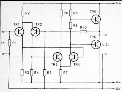
Fig. 3.7 The basic arrangement used in an op. amp. style power amplifier
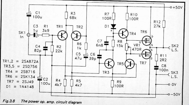
Fig. 3.8
Fig. 3.9 The 50-0-50 volt power supply circuit
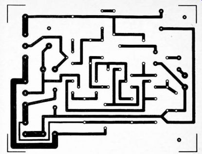
Fig. 3.10 The copper track pattern for the power op. amp. unit
Op Power Amp
Figure 3.8 shows the circuit diagram for a practical power amplifier based on operational amplifier techniques. This follows the lines of the basic operational amplifier circuit discussed previously, but with some changes. Most obviously, the output transistors have been changed for power MOSFETs that enable suitably high output powers to be accommodated.
A constant current generator forms the load for the driver transistor, and part of this circuit also acts as the resistive load for the other transistor in this long-tailed pair. Several resistors and capacitors are needed to ensure good stability. VR1 enables the bias current through the output stage to be trimmed to the correct figure (about 80 milliamps).
This circuit clearly has rather different supply requirements to the power amplifier featured at the beginning of this Section. It requires supplies of plus and minus 50 volts, plus a central 0-volt supply rail, and not a straightforward 100-volt supply. However, it requires few extra components in order to satisfy these modified requirements, and a suitably modified power supply circuit appears in Figure 3.9. Note that whereas the original power supply circuit could operate using either a 30-0-30 volt transformer (or one having twin 30- volt secondary windings), or a 60-volt type, this design will only work using a 30-0-30 volt (or twin 30-volt secondary) type.
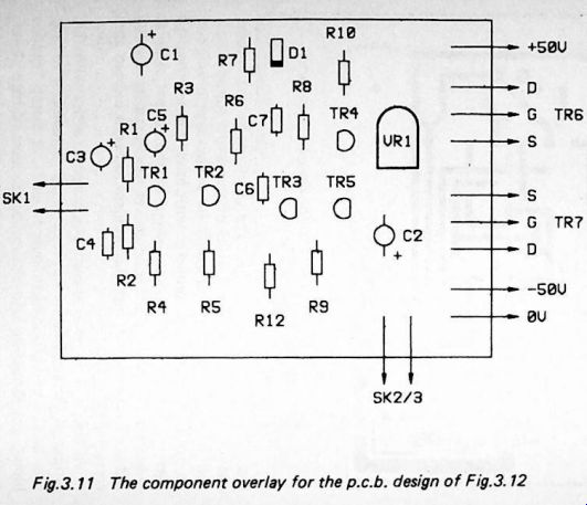
Fig. 3.11
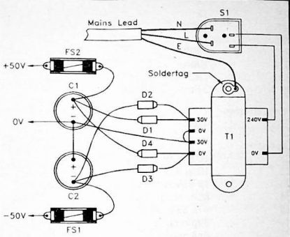
Fig. 3.12
The notes on constructing and setting up the MOSFET power amplifier apply equally well to the present design, and will not be repeated here. Figures 3.10 and 3.11 show the copper pattern and component layout (respectively) for the printed circuit board. Figure 3.12 shows the wiring for the power supply unit.
I would strongly urge that the unit should be tested initially without a load connected across the output. VR1 should be adjusted for a total current consumption from the unit of about 90 milliamps, and either the positive or the negative supply rail can be monitored. The quiescent output voltage should be within about 0.2 volts of the 0-volt supply level, and any offset here will probably be so low that it will not be possible to detect it properly with most multimeters. If there is a significant offset voltage at the output, this is indicative of a fault, and a loudspeaker should not be connected across the output until the problem has been located and corrected.
Although no fuse is shown connected in series with the output of the amplifier, I would certainly recommend adding one in the unit's non-earth output lead. A 3-amp "quick- blow" fuse should be satisfactory. Some users of high power audio amplifiers tend to look down on this practice, which does have its drawbacks. One of these is simply that there will be a small loss of power through the fuse, although this is unlikely to be large enough to be of any real significance in practice. Another problem is that the resistance of the fuse tends to reduce the damping of the amplifier on the loudspeaker.
This is undesirable, but is again something that is not likely to noticeably reduce the performance of the system. The only reason that 1 omitted this fuse from the prototype amplifier was because the loudspeaker system in use incorporated such a fuse. Obviously, if the loudspeaker system includes such a fuse, there is little point in including one in the amplifier.
Components
Power Op Amp (Fig.3.8)
Resistors (all 0.25 watt 5% carbon film)
R1 3k9 R2 22k 68k R3 4k7 R4
4k7 R5 1-k R6 100 R R7 15k R8 100R
100R R9 R10 2R2 R10 27k R12 Potentiometer VR1 470R sub-min hor preset
Capacitors 100 u 63V radial elect 1 00m 63V radial elect Ip 63V radial elect 82p ceramic plate 47p 63V radial elect 39p ceramic plate 6n8 polyester 100n polyester C1 C2 C3 C4 C5 C6 C7 C8
Semiconductors
TR1 TR2 TR3 TR4 2SA872A
2SA872A 2SD756 2SB716 2SD756 2SK134 2SJ49 1N4148 TR5 TR6 TR7 D1
Miscellaneous
SK1 SK2
Standard jack, phono socket, etc.
Terminal post or spring terminal
Terminal post or spring terminal Large (1.2 degrees Centigrade per watt or better) heatsink Two TO-3 insulating kits Printed circuit board Wire, solder, etc.
SK3
Power Supply (Fig. 3.9)
Rotary mains switch
Mains primary, 30-0-30 volt (or twin 30 volt) secondary (refer to text for details of the required current ratings)
1N5402
4700u 63V single ended electrolytic with tag connections
3A (or 3.15A) 20mm quick-blow 3A (or 3.15A) 20mm quick-blow 20mm chassis mounting fuse holders (2 off)
Mounting clips for C1 and C2
Wire, solder, etc.
S1 T1 D1 D2 D3 D4 C1 C2 FS1 FS2
Bridge Circuit
An advantage of using operational amplifier techniques in high power amplifiers is that it makes it easy to obtain a bridge amplifier for even higher output powers. The operational amplifier biasing techniques ensure that the outputs of both amplifiers are within a fraction of a volt of the 0-volt supply level, giving no significant offset voltage across the two outputs. Operational amplifier techniques also make it easy to produce amplifiers that have virtually identical voltage gains, but with one amplifier having an inverting action while the other has a non-inverting action.
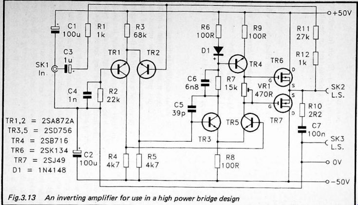
Figure 3.13
The amplifier circuit of Figure 3.8 is well suited to use as one section of a bridge amplifier, and the circuit of Figure 3.13 shows a suitable amplifier circuit for the other side of the bridge. The original circuit is of the non-inverting variety, while the circuit of Figure 3.13 has been modified to give an inverting action. Apart from the change in the feedback network and input circuit to provide an inverting action, this circuit is much the same as the original. Feedback resistors R1, R11 and R12 give a voltage gain of some 28 times, which matches that of the non-inverting amplifier. The input impedance of the amplifier is only about 1-k, and the input impedance of the circuit as a whole (i.e. with both sides of the bridge included) is somewhat lower at approximately 800 ohms. Although this is rather low, any good preamplifier circuit should be able to handle such loading without difficulty.
The output power available from a complementary pair of these amplifiers in a bridge configuration is quite high. The first point that has to be made is that both amplifiers in the bridge should have at least two pairs of power MOSFETs in their output stages. Also, the two amplifiers should be powered from a common power supply circuit, and should not have separate supplies, current rating of about 6 amps or more1 if really high output powers are to be achieved. The load impedance should not be less than 8 ohms. For good stability it is probably best to include a C 100n capacitor) from the output of each amplifier module to the 0-volt supply. This will almost certainly be better than using a single C - R circuit across the loudspeaker.
In theory, with one amplifier capable of delivering around 100 watts r.m.s. into an 8-ohm load, a bridge circuit with two amplifiers should be able to deliver four times this amount.
In practice it is unlikely that these amplifiers in a bridge arrangement will provide as much power as this. The peak output currents are very high, giving significant voltage drops through the output transistors. This reduces the actual maximum output power, but experiments with the prototype equipment would suggest that powers in excess of 300 watts r.m.s. can be readily achieved. I have not tried using more output devices in the amplifiers in order to further boost the output power, but it would seem reasonable to expect output powers of up to about 400 watts r.m.s. to be achievable in this way.
A suitable printed circuit design is shown for the inverting amplifier module in Figures 3.14 (track pattern) and 3.15 (component overlay). Construction and setting up for this amplifier module follow closely along the same lines as those for the non-inverting version of the amplifier, and they will not be described again here.
The mains transformer should have a R circuit (i.e. a 2R2 resistor in series with a 100 n capacitor) from the output of each amplifier module to the 0-volt supply. This will almost certainly be better than using a single C - R circuit across the loudspeaker.
In theory, with one amplifier capable of delivering around 100 watts r.m.s. into an 8-ohm load, a bridge circuit with two amplifiers should be able to deliver four times this amount.
In practice it is unlikely that these amplifiers in a bridge arrangement will provide as much power as this. The peak output currents are very high, giving significant voltage drops through the output transistors. This reduces the actual maximum output power, but experiments with the prototype equipment would suggest that powers in excess of 300 watts r.m.s. can be readily achieved. I have not tried using more output devices in the amplifiers in order to further boost the output power, but it would seem reasonable to expect output powers of up to about 400 watts r.m.s. to be achievable in this way.
A suitable printed circuit design is shown for the inverting amplifier module in Figures 3.14 (track pattern) and 3.15 (component overlay). Construction and setting up for this amplifier module follow closely along the same lines as those for the non-inverting version of the amplifier, and they will not be described again here.
---------------------
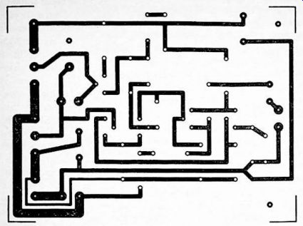
Fig. 3.14 The track pattern for the inverting MOSFET power amplifier.
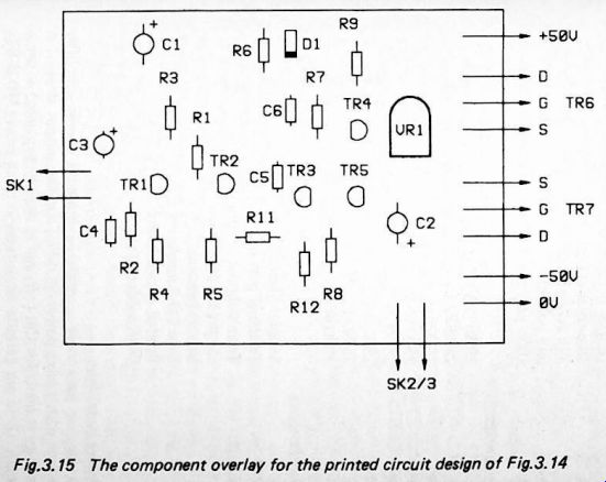
Fig. 3.15
Components Inverting Op Power Amp (Fig.3.13)
Resistors (all 0.25 watt 5% carbon)
1k R1 22k R2 R3 68k 4k7 R4 4k7 R5 R6 100R 15k R7 R8 100R
100R R9 R10 2R2 R11 27k 1-k R12
Potentiometer
VR1 470R sub-min hor preset Capacitors C1 100m 63V radial elect 100^ 63V radial elect
63V radial elect
In polyester 39p ceramic plate 6n8 polyester 100n polyester C2 C3 C4 C5 C6 C7
Semiconductors
TR1 TR2 TR3 TR4 2SA872A 2SA872A 2SD756 2SB716 2SD756 2SK134 (2 off, see text)
2SJ49 (2 off, see text)
1N4148 TR5 TR6 TR7 D1
Miscellaneous
SK1 SK2 SK3
Standard jack, phono socket, etc.
Terminal post or spring terminal
Terminal post or spring terminal Large (1.2 degrees Centigrade per watt or better) heatsink
Two TO-3 insulating kits
Printed circuit board
Wire, solder, etc.
---------------------
Bipolar Amplifiers
So far we have only considered practical power amplifier designs which have power MOSFETs in the output stage. No apology is made for this fact, and as already explained at some length, there are definite advantages in using power MOSFETs rather than ordinary bipolar power transistors. In particular, the lack of any problems with thermal stabilization makes power MOSFETs a good choice for home constructed power amplifier designs.
However, for those who prefer to use bipolar transistors throughout, two bipolar transistor high power circuits are provided here. These are basically just the operational amplifier style inverting and non-inverting circuits described previously, but modified to take bipolar transistors in the output stages. The circuit diagrams for these two amplifiers are provided in Figure 3.16 (non-inverting amplifier) and Figure 3.17 (inverting amplifier).
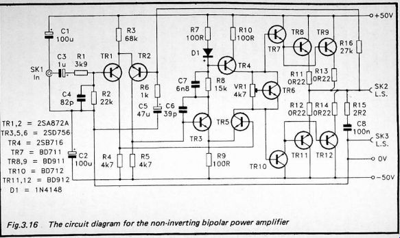
Figure 3.16
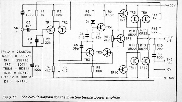
Figure 3.17
The first point to note is that it is not possible to simply replace each power MOSFET with a bipolar power transistor. The current gain of a typical power transistor is only about 50, which is nothing like high enough with a collector current of only about 8 milliamps or so in the driver stage. Either the current flow in the driver stage must be considerably increased, or extra transistors must be used in the output stage in order to boost its current gain. In this case the driver current is left unaltered, and two Darlington pairs are used in the output stage. In fact the second transistor in each Darlington pair is a pair of parallel connected power transistors, complete with emitter resistors. This enables high output currents and powers to be handled more safely, particularly if the amplifiers are used in a bridge configuration.
The choice of output transistors is important in this application, where high frequency performance can suffer if a poor choice is made. Transistors such as the 2N3055, MJE2955, 2N3773, 2N6609, etc., are often used as the output transistors in high power audio amplifiers. In some ways they are less than ideal for this application though. In the case of the 2N3055 and its complements, it should be borne in mind that its Vceo rating is only 60 volts, although it often seems to be used in audio power designs operating with supply voltages as high as 100 volts (or dual balanced 50-volt supplies). When subjected to maximum voltage the device is likely to have a reverse bias, which makes this practice less risky than it might appear, although it is still one that I would not recommend.
Another problem with many high power transistors is that they have cut-off frequencies of only about 200kHz or so.
While this may seem to be adequate for devices that will be used for audio amplification, with an upper frequency limit of 20kHz, it has to be remembered that the F, figure for a transistor is the one at which its gain falls to unity. In other words, it is the frequency at which its gain falls to a level where it is no longer providing any gain at all. The gain of the device starts to fall away at a much lower frequency. For example, if a power transistor has a gain of 50 and an of 200kHz, dividing the Ft figure by the current gain gives the frequency at which the gain of the transistor starts to roll-off.
In this case it is clearly at a frequency of 4kHz (200kHz divided by 50 = 4kHz).
This does not mean that the closed loop gain of the power amplifier will start to roll-off at 4kHz. It is the open loop gain that will suffer from this low roll-off figure. This is reflected in less negative feedback at high frequencies, which gives increased distortion. In most cases it also results in reduced power bandwidth. In other words, at high frequencies the maximum output power falls away slightly, and in a severe case it would only be a small fraction of the maximum output power at middle frequencies. The output of the circuit may well be unable to follow sudden changes in the input level correctly, producing a form of distortion called "slewing induced distortion", or just "SID".
Power transistors intended for use in audio amplifiers are generally engineered to have somewhat higher F_ts of typically about 3MHz. This is the Ft figure for the BD91 1/912s which are recommended for this design. Even with a fairly high current gain figure of around 100, the gain of these transistors will not roll-off until a frequency of about 30kHz is reached.
This ensures good performance over the full audio range. The circuit will work with high power transistors which have lower F_ts, and devices such as the 2N3773 (n.p.n.) and the 2N6609 (p.n.p.) are usable. However, it might be necessary to make some slight adjustments to the values of the compensation capacitors in order to ensure good stability. In order to get the 2N3773 and 2N6609 to function in these designs I found it necessary to add a 33p ceramic plate capacitor across feedback resistor R16. This will presumably be necessary with other low Ft power transistors. I would strongly recommend the use of the BD911/912 or similar devices if at all possible, and can not guarantee that other devices will prove to be entirely satisfactory in this design.
Thermal Stability
Using bipolar output transistors means that there is a problem with thermal stability to overcome. This design uses the standard method, which is to have a transistor in the amplified diode configuration to control the quiescent output bias current. This is based on TR6, and has its output voltage (and hence the quiescent bias current) controlled by VR1. VR1 should be set so that the output bias current is about 110 milliamps, which equates to about 100 milliamps through the output transistors.
Of course, TR6 should be mounted on the heatsink which takes TR8. TR9. TR11 and TR12, so that it responds to their rise in temperature, and stabilizes the output bias current. The output current should be monitored to ensure that it does not rise significantly as the output transistors heat up. If neces
sary, a better thermal contact between TR6 and the output transistors must be obtained in order to prevent a continual rise in the output current. Alternatively, readjusting VR1 to return the current drain to about 1 10 milliamps might give satisfactory results. Note though, that this method will give a low bias current (and possibly high cross-over distortion) each time the amplifier is used, before the output transistors become healed up. Also, it does not absolutely guarantee that thermal runaway will not occur. It is possible that the quiescent current might drop slightly as the output transistors heat up. This would suggest a thermal coupling that is too good, and the coupling to TR6 should then be loosened slightly.
No construction details are provided for these two amplifiers, but they can be constructed along much the same lines as the power MOSFET designs. It would probably be possible to use the same printed circuit designs after a small amount of modification. I tested the prototype amplifiers using the power MOSFET circuit boards plus some hard wiring. This did not give particularly neat finished results, but the amplifiers worked well enough.
Remember that TR7 and TR10 require heatsinks. They can be mounted on the same heatsink as the output transistors if desired, or they can be fitted on their own heatsink (one of about 3 degrees Centigrade per watt should suffice). Bear in mind that the metal tabs of the BD711/712/911/912 transistors connect internally to their collector terminals. It is essential that all these devices should be properly insulated from their heatsinks using TO-220 insulating kits. These consist of a single insulating washer plus one plastic bush (just one bush, since this type of transistor has only one mounting bolt).
These amplifiers produce output powers that are comparable to the power MOSFET circuits, and if anything, they will produce what are generally slightly higher output powers for a given set of operating conditions. I have not made any distortion measurements on the bipolar versions of the amplifiers, and in this respect I would not expect them to be as good as the power MOSFET designs. However, listening tests would suggest that they have quite a reasonable level of performance in this respect, and they should certainly give adequate for most high power audio applications.
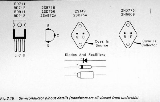
Fig. 3-18
Components
Non-inverting Bipolar Power Amplifier (Fig.3.16)
Resistors (0.25 watt 5% carbon unless indicated)
3k9 R1 R2 22k 68k R3 R4 4k7, 4k7 R5 R6 1k R7 100R R8 15k R9 100R 100R OR22 3 watt OR22 3 watt OR22 3 watt OR22 3 watt R10 R11 R12 R13 R14 R15 2R2 R16 27k
Potentiometer VR1 4k7 sub-min hor preset Capacitors 100u 63V radial elect
63V radial elect
63V radial elect 82p ceramic plate 47^ 63V radial elect 39p ceramic plate 6n8 polyester 100n polyester C1 C2 C3 C4 C5 C6 i C1 '
C8
Semiconductors
TRI TR2 TR3 TR4 2SA872A
2SA872A 2SD756 2SB716 2SD756
2SD756 BD711 BD91 1 BD911 BD712 BD912
BD912 1N4148 TR5 TR6 TR7 TR8 TR9 TR10 TRI 1 TRI 2 D1
Miscellaneous
SKI SK2 SK3 Standard jack, phono socket, etc.
Terminal post or spring terminal
Terminal post or spring terminal Large (1.2 degrees Centigrade per watt or better) heatsink Six TO-220 insulating kits Printed circuit board Wire, solder, etc.
Inverting Bipolar Power Amplifier (Fig. 3.17)
Resistors (0.25 watt 5% carbon unless indicated)
1k R1 22k R2 68k R3 4k7 R4 4k7 R5 100R R6 15k R7 100R 100R OR22 3 watt OR22 3 watt OR22 3 watt OR22 3 watt R8 R9 R10 R11 R12 R13 1k R14 2R2 R15 27k R16
Potentiometer
VR1 4k7 sub-min hor preset
Capacitors 100u 63V radial elect 100m 63V radial elect 4m7 63V radial elect
In polyester 39p ceramic plate 6n8 polyester 100n polyester
C1 C2 C3 C4 C5 C6 C7
Semiconductors
TR1 TR2 TR3 TR4 2SA872A
2SA872A 2SD756 2SB716 2SD756
2SD756 BD711 TR5 TR6 TR7
BD911
BD911 BD712 BD912
BD912 1N4148
TR8 TR9 TR10 TR11 TR12 D1
Miscellaneous
SK1 SK2 SK3
Standard jack, phono socket, etc.
Terminal post or spring terminal
Terminal post or spring terminal
Large (1.2 degrees Centigrade per watt or better) heatsink
Six TO-220 insulating kits
Printed circuit board
Wire, solder, etc.