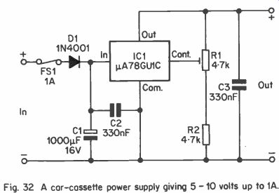
Fig. 32 A car-cassette power supply giving 5-10 volts up to 1A.
| Home | Audio mag. | Stereo Review mag. | High Fidelity mag. | AE/AA mag. |
This section will cover a number of designs for power supplies or power supply related projects, which do not fall into any of the categories covered in the previous sections.
Car-Cassette Supply
If a cassette recorder is being powered from internal batteries, running costs are normally rather high due to the quite high current consumption of these devices (the motor for the deck usually requires several hundred milliamps). If the unit is being used at home, a great saving in running costs can be obtained by running it from the mains supply, either using an internal power supply if one is fitted, or by connecting an external supply to the power socket of the recorder if there is no built in supply. If the recorder is used in a car, it is again possible to obtain greatly reduced running costs, this time by powering the recorder from the car battery.
One problem here is that most car batteries have a nominal potential of 12 volts, whereas most cassette recorders are for 6, 7.5 or 9 volt operation. It is therefore necessary to interpose a voltage stabilizer having the appropriate output voltage, between the car battery and the recorder.
The circuit diagram of a simple regulator which is suitable for this application is shown in Figure 32. This is based on the pA78GU1C device which was covered in the previous section, and the operation of this device will not, therefore, be covered again here. The circuit will provide up to 1 amp (which should be sufficient for any cassette recorder) and the output voltage is continuously variable from approximately 5 volts to 10 volts, which includes the three normal cassette recorder supply voltages of 6, 7.5 and 9 volts.
Fig. 32 A car-cassette power supply giving 5-10 volts up to 1A.
The input voltage is taken to the regulator i.c. via fuse FSI and protective diode, Di. The latter blocks the input from the regulator device if the input is accidentally connected with the wrong polarity. The input voltage is likely to contain a substantial amount of noise, and C1 is used to combat this. Of course, the regulator also provides electronic smoothing of the output, and considerably reduces the noise level on the output; C2 and C3 are the normal decoupling capacitors for the regulator i.c. R1 and R2 form the potential divider which controls the output voltage. The nominal output potential is 5 volts with the slider of R1 at the upper end of its track, increasing to 10 volts (approximately) as it is moved down to the lower end of its track.
Of course, thermal overload protection circuitry and foldback current limiting are incorporated in the µA78GUIC, as mentioned in the previous section. The i.c. should be mounted on a reasonably substantial heatsink, and this could merely consist of the metal case for the project. The heat-tab of the 1.0.78GU1C connects internally to its 'COM' terminal, and it is therefore unnecessary to insulate the heat-tab from the case (and the chassis of the car) in negative earth vehicles. However, it is essential that IC1 is properly insulated from the case and the car's chassis if the vehicle is of the positive earth type, otherwise the supply will be short circuited! If the unit is used in a positive earth car, FS1 should be moved into the negative input lead, so that it protects the unit in the event of a short circuit caused by faulty insulation of IC1.
Components
Car-Cassette
Power Supply (Figure 32)
Resistors
R1 4.7k 0.25 watt preset
R2 4.7k 1/3 watt 5%
Capacitors
C1 1000 uF 16V
C2, C3 330 nF plastic foil (2 off)
Semiconductors
IC1 1.0.78GU1C
D1 1N4001
Fuse
FS1 20mm 1A. quick blow type
Miscellaneous
Case, circuit board, input and output leads, wire, 20mm chassis mounting fuseholder, solder etc.
Train Controller
Most simple train controllers consist of a step-down and isolation transformer driving a bridge rectifier and a large (in terms of wattage, not resistance) variable resistor. One problem with this simple arrangement is that it produces a high output impedance at low and medium speeds, and gives a tendency for the motor to stall. This occurs because an increase in the loading on the motor (caused by the train going up a gradient for example) results in it trying to draw more supply current.
Due to the high output impedance of the supply, the increased loading by the motor causes a significant reduction in the output voltage of the supply, and the supply current only marginally increases. With the supply voltage actually reducing, the power fed to the motor could actually decrease! It then becomes quite likely that the motor will stall.
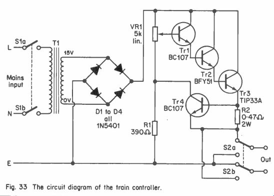
Fig. 33
A better method is to use a stabilized supply having a continuously variable output of 0 to about 12 volts or so, and the circuit of a simple unit of this type is shown in Figure 33.
T1 is the isolation and step-down transformer, and it has a secondary rating of 15 volts at 1.5 amps or more. Its output is full wave rectified by the bridge rectifier formed by D1 to D4, and then this rough d.c. output is fed to a simple voltage controller circuit. This does not provide a highly stable output, and is really just a potentiometer feeding a buffer amplifier. Thus the voltage set on VR1 is transferred to the low impedance output at Tr3's emitter, less the drop of about 2 volts incurred through the three transistors ( Tr1 to Tr3) of the buffer amplifier. This simple arrangement gives adequate output stability for this application.
It is not necessary for the output of the supply to be smoothed, and it is in fact normal for d.c. motor supplies to have a pulsating d.c. output.
Tr4 and R2 provide output current limiting at a little over 1.4 amps (peak), and this protects the unit against damage if an accidental short circuit on the output should occur. S2 can be used to transpose the polarity of the output of the unit, and is the motor reversing switch.
Tr3 will dissipate several watts under certain operating conditions, and must be given a reasonable amount of heatsinking.
Components Train Controller (Figure 33)
Resistors
R1 390 ohms 1/3 watt 5%
R2 0.47 ohms 2 watt 5% VR1 4.7k or 5k lin. carbon
Semiconductors
Tr1 BC107 Tr2 BFY51 Tr3 TIP33A Tr4 BC107 D1 to D4 1N5401 (4 off)
Transformer
T1 Standard mains primary, 15 volt 1.5A. secondary
Switches
S1 D.P.S.T. rotary mains or toggle type
S2 D.P.D.T. toggle type
Miscellaneous
Case, circuit board, control knob, mains lead, wire, solder etc.
Ni-Cad. Charger
Ni-Cad cells are now quite frequently used in battery powered equipment which has a fairly high current consumption, since ordinary batteries require frequent replacement in such applications, and tend to be relatively expensive in the medium and long term. Ni-Cad cells and a suitable charger are admittedly more expensive in the short term, even if the charger is home-constructed at low cost, but this is more than compensated for by the considerable savings that can be obtained over a longer period of time.
A special charger is needed for Ni-Cad cells because they have a very low internal resistance, but must be charged at a fairly low current in order to avoid damage. In practice this means that they must be charged from a constant current source. The circuit shown here (Figure 34) provides a nominal charging current of 50 mA., and is intended for use with the popular AA size cells (which are equivalent to HP7 dry cells in size). These are used in electronic flashguns, cassette recorders, electric toys, and many other applications. The charger can be used to charge up to five cells at a time. When charging more than one cell, the cells should be connected in series across the output, and not in parallel.
The left hand section of the circuit is the normal form of step down isolation, full wave rectifier and smoothing circuit. This provides a loaded output potential of very roughly 17 volts.
The right hand section of the circuit is the constant current generator, and is based on a small 5 volt monolithic voltage regulator. Provided the input voltage is sufficient, the output terminal of IC1 will, of course, be maintained at a nominal potential of 5 volts above the earth rail. This gives a current of about 45 mA. through R1 which is connected across the output of IC1. The current flowing into the input of IC1 will there fore be approximately 45 mA., plus the current consumed by the regulator i.c. itself, which is just a few mA. and brings the total input current to about 50 mA.
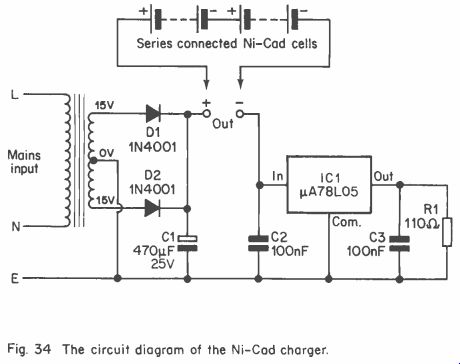
Fig. 34.
Thus, when a Ni-Cad cell or cells are connected across the output terminals of the circuit, or even if a short circuit is placed across the output terminals, IC1 and its associated circuitry will limit the current flow to only about 50 mA., and an excessive current flow is avoided. There is obviously a limit to the number of cells that can be charged from the unit, since the greater the number of cells connected into circuit, the larger the voltage dropped across them, and the lower the voltage fed to the input of IC1. If too many cells are connected to the unit, the input voltage to IC1 will fall` below the minimum level for correct operation (about 7.5 volts), and the Ni-Cads would then receive little or no charge current. Using a component having a secondary rating of 100 mA. in the T1 position it should be possible to charge at least five cells, and six cells can be charged if T1 has a secondary rating of 200 mA. or more.
Plastic battery holders for AA size cells are readily available, and the cells can be fitted into one of these while they are being charged. These battery holders are equipped with a PP3 type connector, and the charger can therefore be fitted with a PP3 battery connector at its output in order to facilitate easy connection to the cells.
The charger can also be used with PP3 size Ni-Cad cells which require a charging current of about 11 mA. T1 needs to have a secondary rating of 100 mA. or more, and R1 should be changed to a 680 ohm component.
Components
Ni-Cad Charger (Figure 34)
Resistor
R1 110 ohms 1/3 watt 5%
Capacitors
C1 470 uF 25V C2, C3 100 nF plastic foil (2 off)
Semiconductors
IC1 78L05 (5 volt, 10 mA. positive regulator)
D1, D2 1N4001 (2 off)
Transformer T1
Standard mains primary, 15-0-15 volt 100 or 200 mA. secondary (see text)
Miscellaneous
Case, circuit board, output connector, mains lead, wire, solder etc.
Electronic Fuse
This simple add-on unit is designed to be connected in the output from a bench power supply, and will cut off the output if a current in excess of some predetermined level is drawn from the supply. It operates extremely rapidly, and is far faster in operation then a conventional fuse. It can also operate at lower currents than is possible with conventional fuses. This unit is ideal for use when experimenting with delicate semi conductor devices which could easily be damaged by an excessive current flow.
The unit will operate on supply voltages of between about 7 and 25 volts, and the trigger current can have any value from a few mA. up to 100 mA. or so. The unit does increase the output impedance of the supply, but this will not be of any serious consequence in the majority of applications. The circuit has a current consumption of about 3.5 mA. at a supply potential of 7 volts, rising to about 12 mA. at a supply voltage of 25 volts (this is in addition to the output current).
Figure 35 shows the circuit diagram of the electronic fuse.
Under normal operating conditions Tr1 is biased hard into conduction by the base current it receives through R3, S2, R2 and D1. Power is therefore coupled from the input to the output by way of Rt and Tr1.
If an excessive output current is drawn from the output of the unit, the voltage developed across Rt becomes high enough to switch on Tr3, and a small base current is supplied to Tr3 via R1. Tr3 then supplies a small base current to Tr2, which is biased into conduction and supplies a base current to Tr3.
This regenerative action continues until both Tr2 and Tr3 are biased hard into conduction. These two transistors are actually connected to form a sort of highly sensitive thyristor. An ordinary thyristor or s.c.r. is not suitable for use here as it would require a rather high trigger current, and would also tend not to give a latching action at the relatively low operating current used here.
The latching action occurs because once triggered, the
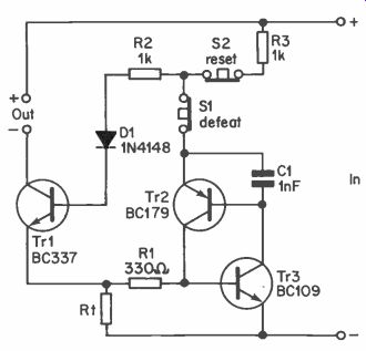
Fig. 35 The circuit diagram of the electronic fuse.
transistors bias each other into conduction and no input bias is needed. Furthermore, even if the current through Rt is reduced to zero, due to the inclusion of R1 neither Tr2 or Tr3 will switch off. R1 and Rt simply act as a collector load resistance for Tr2, and the base voltage of Tr3 remains high enough to keep it conducting heavily.
When Tr2 and Tr3 are triggered, the current through Rt does in fact reduce to zero, because the junction of Si, S2 and R2 is pulled down to only about 1 volt positive of the negative input rail. Due to the inclusion of D1 in the bas... circuit of Tr1, about 1.2 volts is needed at this point in the circuit in order to bring Tr1 to the threshold of conduction. It therefore ceases to conduct, and cuts off the supply to the output.
Once triggered, the cut-out can be reset by operating S2 momentarily. This cuts the supply of current to Tr2 and Tr3, causing them to switch off. The output is then restored when S2 is released (unless the overload is still present on the output, and the circuit will then immediately retrigger).
One problem with this type of circuit is that the circuit can tend to be triggered when an item of equipment is initially connected across the output. This is due to the brief surge of current taken by the decoupling capacitors in the supplied equipment. Operating reset button S2 is of no use as the circuit is simply retriggered each time S2 is released. Defeat switch S1 has therefore been included. When operated, this simply disconnects the thyristor circuitry from Tr1's base feed circuit and the cut-out action is eliminated. This resets the circuit and gives an opportunity for the decoupling capacitors in the supplied equipment to charge up. Some caution is needed before operating S1 though, since both the cut-out and the supplied equipment could be damaged if this switch is operated and there is a genuine overload across the output.
C1 is needed merely to prevent spurious operation of the highly sensitive thyristor circuitry.
The value of Rt must be varied to give the required trigger current. Its value is equal to 0.5 divided by the required trigger current in amps (or 500 divided by the required trigger current in milliamps). In either case the value of Rt is given in ohms. The answer is unlikely to coincide with a preferred value, but it is then merely necessary to choose the nearest preferred value. If, for example, a trigger current of 100 mA.
is required, this gives a calculated value of 5 ohms, and in practice a 5.1 ohm component would be used, or a 4.7 ohm type might be a better choice as this is in the El 2 series of preferred values and is more readily available.
Components Electronic Fuse (Figure 35)
Resistors. (All 1/3 watt 5%)
R1 330 ohms
R2 1k
R3 1k
Rt see text
Capacitor
C1 I nF ceramic plate
Semiconductors
Tr1 BC337
Tr2 BC179
Tr3 BC109
D1 1N4148
Switches
S1 Push to break, release to make type
S2 Push to break, release to make type
Miscellaneous
Case, circuit board, input and output sockets, wire, solder etc.
Supply Splitter
This device can be used to produce dual balanced supplies from a single supply, and thus enables operational amplifier circuits requiring dual rails to be powered from ordinary bench power supplies. The unit will operate with input voltages of between 12 and 30 volts (36 volts is the absolute maximum input voltage), and gives outputs of between + 6 volts and + 15 volts. Output currents of up to about 200 mA. or so can be comfortably handled by the circuit.
The circuit diagram of the unit is given in Figure 36. The circuit is based on IC1, which is a Class B power amplifier device that is really a form of high power operational amplifier. R1 and R2 form a fairly high impedance center tap on the input rails, and IC1 is connected as a unity gain buffer amplifier which is fed from this center tap. Half the supply potential therefore appears at the output of IC1, and this part of the circuit is at a very low impedance. If this point is made the OV. rail, the positive and negative input rails then act as the output rails which are positive and negative respectively to the central earth rail. Of course, each output rail is at a potential of only half the input voltage.
C1 to C3 are needed to limit noise level on the output, and to pi event instability.
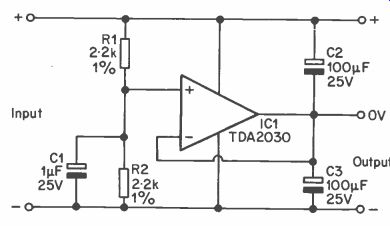
Fig. 36 The circuit diagram of the supply rail splitter.
One problem with this type of circuit is that the 0V. rail can only be earthed if the supply has a separate earth socket, and the mains earth is not permanently connected to one or other of the output rails. Many bench supplies have the mains earth connection taken to a separate output socket, so that the appropriate output rail can be earthed, or neither of them are earthed, as circumstances dictate. Another method is to have a 3 way rotary switch which is used to connect the mains earth to negative rail in the first position, the earth socket when in the central position, and the positive rail when in the third position. With either of these two systems, both of which can be applied to the bench power supply designs in this guide, there is obviously no problem when using the supply splitter unit. Note that when one of the earthing arrangements mentioned above is used, the chassis and case of the supply must still be permanently connected to the mains earth lead in the interests of safety.
Components
Supply Rail Splitter (Figure 36)
Resistors. (All 1/2 watt 2% or better)
R1 2.2k
R2 2.2k
Capacitors
C1 1 µF 25V
C2, C3 100µF 25V (2 off)
Semiconductor
IC1 TDA2030
Miscellaneous
Case, circuit board, input and output sockets, wire, solder etc.
D.C. Step-Up
It can sometimes be necessary to power (say) a 9 volt radio from a 6 volt battery supply, and some form of step up voltage circuit is then required. One way around this is to use an oscillator powered from the low voltage input and feeding into the primary winding of a step-up transformer. The output of the transformer is then smoothed and rectified to give the higher d.c. output voltage.
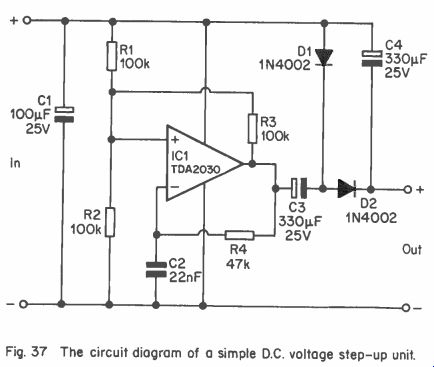
Figure 37
This is not the only method though, and the simple arrangement of Figure 37 can be used where only a modest voltage step-up is required. IC1 is used in a squarewave oscillator circuit, providing a low impedance output at a frequency of a few hundred Hertz. The output signal is coupled by C3 to a simple smoothing and rectifier circuit consisting of D1, D2 and C4. This circuit produces a positive output with respect to the positive rail. In a theoretically perfect circuit the voltage across C4 would be equal to the input voltage, and the voltage across the output of the unit (which consists of the input voltage in series with the voltage across C4) would be double the input voltage. This is not achieved in practice of course, due to the voltage drop through the rectifiers, and because the peak-to-peak output voltage swing of IC1 is considerably less than the input voltage.
From a 6 volt input the prototype produced an output voltage of about 8 volts or so, and good results were obtained when powering a 9 volt radio from a 6 volt source via the step-up circuit. From a 12 volt supply the output is about 18 volts or so, and an output of 24 volts can be obtained from an input potential of about 16 volts. Although the TDA2030 device is not intended to operate from a supply as low as 6 volts, three of these i.c.s were tried in this circuit and all functioned perfectly well with inputs of less than 6 volts.
The maximum current that the unit can supply is well over 100 mA., but it may be necessary to fit IC1 with a small heatsink if the unit is used to continuously supply currents of about 100 mA. or more.
Components
D.0 Voltage Step-Up Unit (Figure 37)
Resistors. (All 1/3 watt 5%)
R1 100k
R2 100k
R3 100k
R4 47k
Capacitors
C1 100 µF 25V
C2 22 nF plastic foil
C3 330µF 25V
C4 330 uF 25V
Semiconductors
IC1 TDA2030
D1, D2 1N4002 (2 off)
Miscellaneous
Case, circuit board, input and output sockets, wire solder etc.
Shaver Inverter
This circuit (Figure 38) enables a 240V mains operated shaver to be operated from a 12 volt battery, such as a car or boat battery. It is important to note that it is only capable of supplying a few watts, and is therefore unsuitable for use with virtually any other mains appliance. The circuit consumes about 500 mA. under quiescent conditions, rising to very roughly 1 amp. under load.
The circuit uses IC1 to generate a low impedance squarewave at a frequency of approximately 50 Hertz, and this is then coupled to step-up transformer T1 by way of d.c. blocking capacitor C3. C4 is a filter capacitor which helps to give a better output waveform. The output is not a sinewave, but is adequate for this application.
T1 is an ordinary mains transformer having a secondary voltage of about 4 to 4.5 volts, and a current rating of about 1 to 2 amps. It is, of course, used in reverse so that the required voltage step up is obtained. It may be difficult to obtain a suitable transformer, but surplus component retailers and specialist transformer suppliers should be able to supply a suitable component.
Note that T1 requires a secondary voltage (or primary voltage as it actually is in this case) of about 4 to 4.5 volts, and not 12 volts. This is due to the fact that although the nominal input voltage is 12 volts d.c., and in practice will normally be a little more than this, say typically 13 volts, there is not an output of 12 volts peak-to-peak, which in terms of r.m.s. voltage is about 4.3 volts.
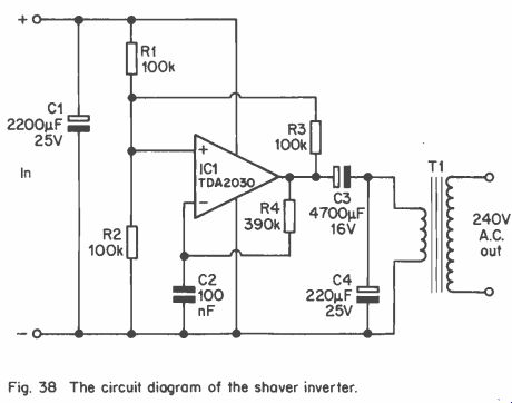
Figure 38.
Bear in mind that the output of the unit is at a fairly high voltage, and although it is also at a fairly high impedance and is not as dangerous as the mains supply, it is nevertheless capable of delivering a severe electric shock. The unit should therefore be constructed so that there is no risk of an accidental electric shock being experienced.
IC1 has to dissipate several watts and it must therefore be mounted on a large heatsink having a rating of only about 2 degrees Celsius per watt or less.
Components Shaver Inverter (Figure 38)
Resistors. (All 1/3 watt 5%)
R1 100k
R2 100k
R3 100k
R4 390k
Capacitors
C1 2200µF 25V
C2 100 nF plastic foil
C3 4700µF 16V
C4 220µF 25V
Semiconductor
IC1 TDA2030


---
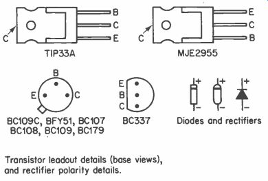
TIP33A B C MJE2955
BC109C, BFY51, BC107 BC337
Diodes and rectifiers
BC108, BC109, BC179
Transistor leadout details (base views), and rectifier polarity details.
--------------------
Transformer
T1 see text
Miscellaneous
Case, circuit board, output socket, wire, solder etc.
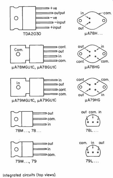
------- Integrated circuits (top views).
Index | Prev. | Next