In the previous Section 1 mentioned that there was a form of active infrared sensor which relies on infrared pulses from the transmitter being reflected back to the receiver by the target object. Systems of this type have a severe drawback in that they provide what is normally only a very limited maximum operating range. With an ideal target object, which would be a highly polished mirror positioned so as to reflect the signal from the transmitter straight back of the receiver, a range of several meters can be achieved. Under practical operating conditions the target object is likely to be far less co-operative than this, and a maximum operating range of around half a meter to one meter would be a more realistic expectation. With a target object that is a very poor reflector of infrared the range could well be very much less than this.
Despite the range limitations, units of this type do have practical applications, and in particular they are popular in the field of robotics. They can be used to give a robot a very simple "eye" which gives warning if it is about to run into something. This is very much better than the common alternative of using microswitches to act as collision detectors, as the microswitch method is rather a case of "shutting the stable door after the horse has bolted", whereas the infrared detector system enables possible disaster to be avoided. There are other applications for this type of infrared detector system, such as detecting that a car is within a certain distance of the rear wall of a garage, and to give warning that it should be taken no closer.
System Operation
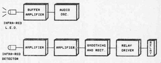
Fig. 26. Block diagram for the active infrared sensor.
A detector of this type can be very simple and inexpensive, and Figure 26 shows the block diagram for a basic system. The transmitter is just an oscillator operating at a fairly high audio frequency and driving an infrared light emitting diode via a buffer stage. The latter is needed because the diode has to be driven at quite a high current in order to give enough reflected signal for reasonable results. The exact operating frequency of the transmitter is not important, but it needs to be fairly high so that the receiver can easily distinguish between the pulse signal and any background noise. In particular, the pulse signal must be easy to separate from 100Hz "hum" from mains powered filament lamps. On the other hand, if the operating frequency is made too high the infrared transmitter and detector devices will provide less than optimum efficiency, as probably will other parts of the system. A frequency of somewhere around 10kHz offers a good compromise.
The point of using a pulsed signal is that this type of signal can easily be detected and used to operate a relay or some other output device. A straightforward DC signal to the transmitting diode would produce an equally strong reflected signal from the target object, but the minute DC signal from the infrared sensor device would be very difficult to detect reliably. Apart from problems with drift in the detector circuit causing spurious operation of the unit, changes in the ambient infrared level could (and probably would) have the same effect. With the pulsed beam system the ambient infrared level is irrelevant unless it becomes so high the sensor becomes saturated, which is never likely to happen in practice.
At the receiver the sensor feeds into a two stage high gain amplifier, and the output pulses from this are rectified and smoothed to give a DC signal that is roughly proportional to the strength of the received signal. This DC signal is used to operate a relay via a simple driver circuit, but under quiescent conditions there will be no significant signal picked up by the sensor, the DC bias signal will be negligible, and the relay will not be activated.
With a suitable target object within range the DC bias signal becomes quite strong, and the relay is activated.
Transmitter
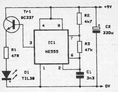
Fig. 27. The circuit diagram for the active infrared sensor transmitter
The circuit diagram of the transmitter appears in Figure 27, and this is basically just a 555 timer used in the astable (oscillator) mode. It provides a roughly squarewave output at a frequency which is set at about 5kHz by timing components R2, R3, and C1.
Tr1 is an emitter follower buffer amplifier which drives infrared light emitting diode D1 by way of current limiting resistor R1. The buffer stage may seem to be unnecessary as the NE555 is capable of directly supplying quite high output currents. However, in practice it seems to be possible to set the drive current more consistently if the buffer stage is included. The drive current to D1 is approximately 100 milliamps, but as the current is switched off for about 50% of the time the average drive current is around 50 milliamps. The current consumption of the circuit as a whole is slightly higher at around 58 milliamps.
Components for Active IR Sensor - Transmitter (Fig. 27)
Resistors (all 1/4 watt 5%)
R1 47R, R2 4k7, R3 47k
Capacitors
C1 C2 3n3 polyester layer 330µ 16V elect
Semiconductors
ICI NE555
Tr1 BC337
D1 TIL 38
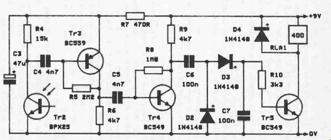
Fig. 28. The circuit diagram for the active infrared sensor receiver unit
Receiver
Figure 28 shows the full circuit diagram for the receiver.
The infrared detector is Tr2, and this is a BPX25 photo-transistor. This device is not specifically intended for infra- red applications, and it has quite good sensitivity in the visible light spectrum (as does not incorporate an infrared filter). Like most opto devices, its peak response is in the infrared part of the spectrum, and it offers good sensitivity when used in the current application. It is aided in this respect by a built-in lens which' increases the light gathering area of the device. This increased pick-up is obtained at the expense of increased directivity, but a sensor having strong directional properties is no real drawback in this application. Although a BPX25 is specified for the Tr2 position of this circuit, similar devices such as the BPY62 and TIL81 seem to work equally well. Note that no connection is made to the base terminal of Tr2.
In infrared applications that involve the reception of pulsed signals the most common type of sensor is a large area photodiode specifically intended for use in infrared remote control and active sensing systems. In this case I did not find one of these devices (a TIL100 to be precise) gave such good results as a phototransistor having an integral lens. This is presumably due to the lack of a lens to give the photodiode strong directional properties and effective gain. Readers who like to experiment with their projects might like to try a TIL100 or similar photodiode in the circuit, together with a suitable lens system. The diode simply connects in place of Tr2 with the cathode connected in place of Tr2's collector terminal, and the anode connected in place of Tr2's emitter. The lens needs to be a convex or double convex type, used in the same way as the one in the in the infrared beam project featured in the previous Section, but at the wavelengths involved here a lens for use with visible light should function quite well and there is no need for a special infrared type.
The output pulses from the sensor circuit will often be only a few millivolts peak to peak in amplitude, or when the unit is used at extreme range the output signal here might be slightly under one millivolt peak to peak. Tr3 and Tr4 are both operated as high gain common emitter amplifiers and they give a total voltage gain of over 80dB (10000 times). When a suitable target object is within range this gives an output signal from Tr4 of a few volts peak to peak, and when this is rectified and smoothed by D2, D3 and C7 it produces a sufficiently strong positive DC bias to take Tr5 into conduction. The latter then activates the relay, which in turn activates the controlled equipment via suitable contacts. In some applications a logic compatible output may be preferable to the relay, and in this case D4 and the relay can be omitted, and Tr5 can be used as an open collector output to pull a TTL logic input low when the unit is activated.
Components for Active IR Sensor - Receiver (Fig, 28)
Resistors (all 1/4 watt 5%)
R4 15k R5 2M2 R6 4k7 R7 470R R8 1M8 R9 4k7 R10 3k3
Capacitors
C3 47p, 16V elect
C4 4n7 polyester
C5 4n7 polyester
C6 100n polyester
C7 100n polyester
Semiconductors
Tr2 BPX25 Tr3 BC559 Tr4 BC549 Tr5 BC549
D2 1N4148 D3 1N4148 D4 1N4148
Miscellaneous
RLA1 Relay with coil suitable for 9 volt operation and coil resistance of about 200R or more (contacts and ratings as required).
Construction
Although construction is not difficult in most respects, there is a potential pitfall in that the receiver has a fairly high sensitivity which leaves it vulnerable to stray pick up and feedback which could cause instability. Taking the stray feedback first, the output of the amplifier at Tr4's collector is in -phase with the input at Tr3's base, and the component layout must be designed to give good isolation between these with no easy feedback paths. Less obviously, feedback to the base of Tr2 can also cause problems, despite the fact that there are no connections to this terminal and it is not forward biased.
The problem of stray pick up other than feedback is mainly one of the signal from the transmitter being received at the receiver via stray electrical pick up rather than by way of reflected infra- red signals. There should be no major problem in avoiding excessive pick up of this type, and it is mainly a matter of leaving a gap of about 10 millimeters of more between the transmitter and receiver circuits, and preferably having an earth plane on the board to provide a degree of screening between the two circuits. It is also advisable to keep leads at the output of the transmitter and the input of the receiver as short as possible, especially the wiring around R4, Tr2, CA, Tr3 and R5.
Another point to keep in mind is that direct optical pick up of the transmitted infrared signal must be kept to a minimum. The directional properties of the transmitting and receiver photocells help in this respect, but the sensitivity of the circuit is such that if any optical path is left between the transmitting LED and receiving phototransistor then the infra- red pulses will find it. It is not just direct pick up straight between the two that has to be contended with, but due to the short distance between the photocells light reflected via (say) the circuit board can also block the system. The best way around this problem is to use small opaque tubes of some kind to shield both the transmitting and receiving photocells. Any stray optical pick up should then be totally insignificant.
The two photocells should ideally be positioned quite close together (around 40 millimeters or so apart), but the exact distance does not seem to be too critical. The prototype readily detected my hand at a range of half a meter or so, which is about as good as can reasonably be expected from a unit of this type. In some circumstances only a very short operating range may be required, and the sensitivity of the unit can then be reduced by making R1 at the transmitter higher in value. In theory, each time the value of this component is raised by a factor of four, the range of the unit is halved. By making R1 much higher in value there is the benefit of a significantly reduced current consumption from the transmitter circuit.
Audio Isolator
Opto-isolators tend to be regarded as strictly for use in triac drive circuits where a mains load is being controlled, and the driver circuit must be isolated from the mains for safety reasons.
However, these devices can (and often are) used in applications where digital or audio signals must be coupled from one circuit to another with no electrical connection between the two. This is not invariably done to provide isolation from the mains supply, but say in the case of digital signals it may be done in order to prevent problems with earth loops (as in the MIDI musical interface for example). With audio signals earth loops can also be a problem, and an opto-isolator can be used to avoid these. Audio isolator circuits are more commonly used though in applications where an audio output is required on a piece of equipment (such as a television set) which has a "live" chassis.
The audio isolator circuit described here can be used either to avoid earth loops or to give isolation from a "live" chassis. It has to be emphasized that if it is used for mains isolation purposes it is imperative that the person installing the circuit knows exactly what he or she is doing, as errors would be potentially very dangerous, and could even have fatal consequences. When used in this way it is therefore a project that should only be undertaken by suitably experienced constructors. Of course, if it is only being used to eliminate an earth loop, then there should be no safety hazard and those of relatively limited experience should have no difficulty in building and installing the unit.
Operating Principle
On the face of it there should be no difficulty in coupling an audio signal through an opto-isolator. All that is needed is a bias circuit at the input of the device so that the audio signal modulated the input current, and then at the output side the device dumps its varying output current into a load resistor. The original audio signal is then produced across the load resistor, or it is in theory at any rate. Unfortunately, in practice the linearity through an opto isolator is generally quite poor, and the resultant audio quality tends to be far from hi-fi. In fact it would probably not even qualify as acceptable mid-fi, and the distortion level could be very high indeed.
Better results can be obtained using a system of frequency modulation or pulse width modulation. Both of these methods transmit a pulse signal through the opto-isolator, and linearity through the device (or lack of it) therefore has no significant affect on the audio output quality: Both systems are perfectly practical for this application, but pulse width modulation is perhaps slightly simpler, and can provide excellent results using quite low cost components. The unit described here is of the pulse width modulation variety.
The block diagram of Figure 29 helps to explain the way in which the system functions. The input signal is fed to one input of a voltage comparator via a lowpass filter. The audio signal is modulated onto a carrier wave which is at an ultrasonic frequency, and the purpose of the lowpass filter is to prevent any high frequency signals from reaching the modulator where they could produce heterodyne whistling sounds on the output signal. In most cases there will be no significant high frequency content on the input signal anyway, but it is advisable to include the input filter just in case. Also, stray pick up of radio signals in the input wiring can sometimes lead to problems, and these can be avoided by the inclusion of the lowpass filter.
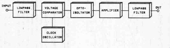
Fig. 29. Block diagram for the audio isolator.
A clock oscillator feeds into the other input of the voltage comparator, and this provides a triangular output waveform at a frequency of around 80kHz. This arrangement gives the required pulse width modulation, and the waveforms of Figure 30 show the way in which this operates. In (a) the audio input to the voltage comparator is at its normal quiescent level, which is half way between the peak voltages of the clock signal. When the clock signal is at the higher voltage the output of the comparator goes high, and when the clock signal is the lower of the two input voltages the comparator's output goes low. This gives a squarewave output with a perfect one to one mark -space ratio, and an average output voltage that is equal to about half the supply potential. In (b) the bias voltage has been set much higher, and as a result of this the clock signal exceeds the input voltage on only a small part of each half cycle. The output signal is consequently a series of much narrower pulses than before, and the average output voltage is much lower. The bias level has been reduced in (c), and consequently the clock signal is at a higher level than the bias voltage for the majority of the time. This results in an output signal that is a series of relatively long pulses, and the …
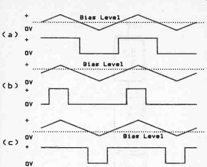
Fig. 30. Modulator output waveforms for various bias levels.
… average output voltage is much higher than with the bias voltage at its normal level.
The point to note here is that by varying the input voltage, the average output voltage of the comparator is varied as well. In this example an increase in the input voltage produces a reduction in the output voltage, and a lower input voltage gives a higher output voltage. This simply means that there is an inversion through the modulator, which is of no practical consequence. This inversion would in fact be avoided if the inputs to the comparator were to be swopped over.
In practice the input signal is a varying voltage rather than a series of fixed voltages, but provided the clock frequency is at least double the maximum input frequency, the average output voltage will vary in sympathy with the input voltage. Figure 31 shows the way in which the pulsed output waveform changes with a triangular input signal supplied to the modulator.
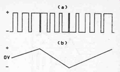
Fig. 31. Output waveform (a) is produced by input waveform (b)
Although this system does not guarantee good linearity, provided the clock signal has good linearity and the comparator has sufficiently fast rise and fall times, good results will be obtained.
Returning to Figure 29, the output from the comparator is applied to the input of the opto-isolator, and here it pulses an infrared LED. On the output side of the opto-isolator there is a phototransistor, and this provides an output signal that does not bear a great deal of resemblance to the input signal. The reason for this is the relatively slow switching speed of an ordinary inexpensive opto-isolator. There are relatively expensive high speed types that could be used, but a more simple and cheaper alternative is to use an ordinary opto-isolator in conjunction with an amplifier, and this combination can provide a good quality output which retains the mark -space ratio of the original signal and which has suitably fast rise and fall times.
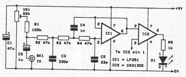
Fig. 32. The circuit diagram for the input filter and comparator.
The final stage is a lowpass filter, and this smoothes the pulses to give an output potential that is equal to the average voltage of the pulse signal, or the wanted audio output signal in other words.
Modulator Circuit
The main circuit diagram for the modulator section of the unit appears in Figure 32, but the clock oscillator circuit diagram is shown separately in Figure 33.
Taking Figure 32 first, the input filter is a conventional third order (18dB) per octave active type based on IC1. VR1 sets the input bias level, and this is adjusted to give optimum large signal handling from the unit. This is more a matter of setting a suitable bias level for the comparator than for the input filter, and the comparator is driven directly from the output of IC1.
The voltage comparator is, of course, IC2, and this is a CA3130E operational amplifier. This device is an externally compensated type, but in this case it is operated open loop and the highest possible slew rate is required, and consequently no compensation capacitor is included. When used open loop the CA3130E is perfectly stable without including this capacitor. D1 Is the LED in the opto-isolator which is an Inexpensive TIL111 type (or any near equivalent). R5 is the current limiting resistor for D1, and it sets the LED current at only about 5 milliamps or so.
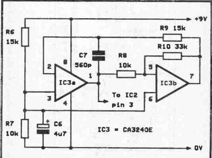
Fig. 33. The circuit diagram for the clock oscillator.
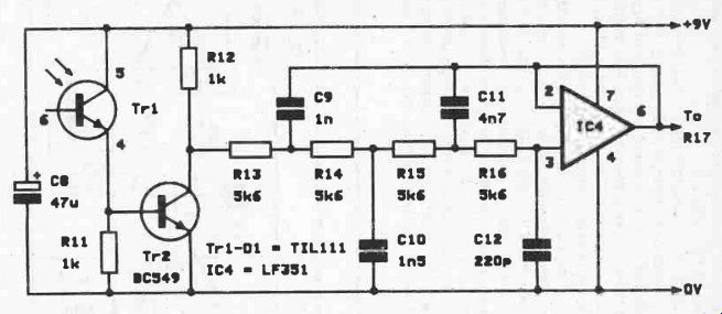
Fig. 34. The circuit diagram for the amplifier and main filter.
Turning now to Figure 33, this is a conventional oscillator circuit of the type which uses a Miller Integrator (IC3a) and a Schmitt Trigger (IC3b). This gives a squarewave signal from the output of IC3b, and the triangular signal that we require in this application is available at the output of IC3a. R6 and R7 provide a bias voltage for the circuit, and this voltage is somewhat less than the usual mid-supply level. This is done in order to compensate for a lack of symmetry in IC3's output stages, and to consequently improve the output waveforms. Due to the fairly high operating frequency of nearly 80kHz it is essential to use a device in the IC3 position that has both a fairly wide bandwidth and a high slew rate. The bias potential must also suit the output characteristics of the device used in the IC3 position. For these reasons the use of other dual operational amplifiers in the IC3 position is not recommended, and would almost certainly produce inferior results.
Fig. 35. The circuit diagram for the output filter.
Figure 34 shows the main circuit for the output side of the circuit, but an additional filter circuit is shown in Figure 35. Of course, these circuits have no electrical connection with those of Figures 32 and 33. They must be powered from separate 9 volt supplies and the 0 volt earth rails must not be connected.
Otherwise the unit becomes pointless and there is no electrical isolation through the circuit.
Tr1 is the phototransistor in the opto-isolator, and it is used to directly drive the base of common emitter switching transistor Tr2. Load resistor R11 ensures that leakage currents in Tr1 can not hold Tr2 permanently switched on. The lowpass filter is a straightforward fourth order (24dB per octave) type having a cutoff frequency of about 20kHz. This gives a reasonably ripple-free output signal, but for really good results some further filtering is required. This is the purpose of the circuit shown in Figure 35, which is a third order lowpass filter, again having a cutoff frequency of about 20kHz. The two filters have a combined attenuation rate of some 42dB per octave, and with the clock frequency almost two octaves higher than the cutoff frequency, this gives around 80dB of clock attenuation at the output.
The importance of the degree of clock attenuation depends on just what will be connected to the output of the unit. With headphones a very high level of ripple is often unimportant, and most headphones can actually be driven direct from a pulse width modulated signal. This is possible as the frequency response of the headphones is not sufficient to permit them to reproduce the clock signal, and they consequently respond to the average output voltage, effectively providing their own lowpass filtering. If the output is going to be connected to an amplifier it is generally necessary to have a low level of ripple on the output signal. There is otherwise a risk of instability in the amplifier, and there could also be problems if the loudspeakers are multiway types having "tweeters". At best there would be a loss of fidelity, and at worst the tweeters would burn out due to the strong clock signal being directed to them.
The unit can drive most types of headphones satisfactorily, and it is generally best if high impedance types have the two phones wired in parallel and low or medium impedance types have series connection. With low impedance types it will probably be beneficial to wire a resistor of about 47 ohms in value in series with C16 to attenuate the output signal somewhat. Of course, stereo headphones can be accommodated, but only by using two isolator circuits, one to handle each stereo channel.
The input signal should be around 1 to 2 volts peak to peak.
Input levels much above 2 volts peak to peak will cause clipping and serious distortion, and with sources of this type an input attenuator must be used to reduce the input signal to an acceptable level. There is about 6dB of voltage gain through the unit incidentally, so the maximum output level is a little over 4 volts peak to peak.
Provided an appropriate input level is used the unit will provide an excellent signal to noise ratio and quite low distortion levels.
The filters in the unit have a 20kHz cutoff frequency, but their cumulative effect provides an overall frequency response which falls slightly short of the full audio bandwidth. However, probably few people have hearing which is sufficiently good to notice the very slight shortfall, and in many cases the source signal will not merit the full bandwidth of the unit anyway. When testing the unit with a high quality FM radio source there was very little discernable difference between the direct signal and the one taken via the isolator.
Components for Audio Isolator (Figs. 32, 33, 34 and 35)
Resistors (all 1/4 watt 5%)
R1 100k R2 47k R3 47k R4 47k R5 1k R6 15k R7 10k R8 10k R9 15k R10 33k R11 1k R12 1k R13 to R19 5k6 (7 off)
Potentiometer
VR1 22k sub -min hor preset
Capacitors
C1 47/h 10V elect
C2 1k 63V elect
C3 330p ceramic plate
C4 in polyester
C5 33p ceramic plate
C6 4µ7 63V elect
C7 560p ceramic plate
C8 47/A 10V elect
C9 in polyester
C10 1n5 polyester
C11 4n7 polyester
C12 220p ceramic plate
C13 3n3 polyester
C14 4n7 polyester
C15 330p ceramic plate
C16 470/1 10V elect
Semiconductors
IC1 LF351 IC2 CA3130E IC3 CA3240E IC4 LF351 IC5 LF351 Tr1-D1 TIL111 or similar opto-isolator Tr2 BC549
Miscellaneous
SK1 3.5mm jack socket SK2 3.5mm jack socket
Circuit board, 8 pin DIL IC holders (2 off), wire, solder, etc.
Stroboscope
A conventional stroboscope uses some form of gas discharge tube to provide bright flashes of light at the required frequency, which can be anything from a few Hertz to (typically) a few hundred Hertz. The general idea of units of this type is to aim the light pulses at a piece of machinery which is in otherwise dark conditions. By synchronizing the frequency of the flashes with the movement of the machinery, the movement appears to be "frozen". If synchronization is not quite perfect the effect is to give the impression that the machinery is running in slow-motion, either forwards or backwards, depending on whether the stroboscope is running slightly too slow or too fast.
These days there is an alternative to the usual gas discharge tubes in the form of so called "super-bright" and "ultra-bright" light emitting diodes. It has to be admitted straight away that these devices do not provide an output level equal to that produced by most gas discharge tubes, even if a number of them are used and they are driven with a high pulse current. On the other hand, they are a far cry from the original light emitting diodes which often failed to glow noticeably even under moderately bright conditions. The best of the very high brightness types give an output which is around one hundred times brighter than a standard LED driven at the same current. To be precise, the output is about 250mcd for one of the best ultra-bright types, as opposed to around 2mcd for a standard 5 millimeter red LED. 3 millimeter diameter LEDs generally have much lower light output levels than the 5 millimeter variety, and I would not recommend the use of 3 millimeter LEDs in this application. As an indication of just how good these ultra-bright LEDs are, under normal indoor lighting conditions one of these devices can shine a beam of light onto a wall one meter away if it is driven at something approaching its maximum current rating.
LEDs are an attractive proposition for a stroboscope as they can operate at quite high frequencies and require nothing elaborate as far as the driver circuit and the power supply are concerned. Although their light output is still relatively limited, it is sufficient to give usable results in most circumstances, and a device of this type certainly represents an interesting and unusual project that can be constructed at quite low cost.
Circuit Operation
Figure 36 shows the circuit diagram of a simple LED stroboscope.
It is basically just a 555 timer device used in the astable mode to generate a series of brief pulses which are fed to the ultra-bright LEDs. With a standard 555 astable the high output time is longer than the low output duration as the output goes to the high state during the charge period, and low while the timing capacitor is discharging. The capacitor is charged via both of the timing resistors, but it discharges through just one, and the charge part of the cycle must therefore be longer.
There is more than one way around this problem, but in this case steering diode D3 is used to effectively bypass R5 and VR1 during the charge period, and the charge rate is then controlled by the series resistance of R3 and R4. Both components have been made comparatively low in value so that the charge time is kept suitably short. During the discharge part of each cycle D3 blocks any significant current flow through R4, and the discharge rate is controlled by the relatively high series resistance of VR1 and R5.
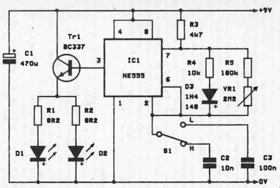
Fig. 36. The circuit diagram for the LED stroboscope.
The circuit therefore provides the required brief positive output pulses at a frequency which can be controlled by VR1. S1 enables one of two timing capacitors to be selected (C2 and C3), and these provide the unit with two frequency ranges. The approximate frequency coverage is 5 to 50 Hertz on the low ("L") range, and 50 to 500 Hertz on the high ("H") range. When dealing with machinery it is more normal to talk in terms of revolutions per minute (RPM) than frequency in Hertz, and in RPM terms the two ranges cover from about 300 to 3000 RPM, and 3000 to 30000 RPM, which should cover most requirements.
Tr1 acts as an emitter follower buffer stage at the output of IC1, and it drives two ultra-bright LEDs (D1 and D2) by way of separate current limiting resistors (R1 and R2). The current through each LED is quite high at something in excess of 500 milliamps, and on the face of it this is far too high for these two components to survive. In fact it gives an excessive current flow in Tr1 as well. In practice Tr1 and both of the diodes survive the experience as the pulses are very brief with a much longer period from one to the next. This results in a very much lower average output current which is always less than 50 milliamps per diode, and comfortably within the capabilities of these components.
C1 is a supply decoupling capacitor, and it has been given a fairly high value so that it can provide the large pulse of current needed on each strobe if the power supply should tend to sag under the heavy loading. It is important that the supply is capable of delivering these bursts of high current as without them the LEDs will lack the required brightness.
Components for LED Stroboscope (Figs. 36)
Resistors (all 1/4 watt 5% unless noted otherwise)
R1 8R2 (1W)
R2 8R2 (1W)
R3 4k7
R4 10k
R5 180k
Potentiometer
VR1 2M2 linear
Capacitors
C1 470µ 10V elect
C2 10n polyester
C3 100n polyester
Semiconductors
IC1 NE555
Tr1 BC337
D1 5mm ultra-bright LED
D2 5mm ultra bright LED
D3 1N4148
Miscellaneous
S1 SPDT toggle switch
Case, circuit board, connecting wire, etc.
Construction and Use
The unit is very simple and there is really nothing that should prove at all difficult as far as construction is concerned. In use it has to be borne in mind that the light output of the unit is quite low, and it will therefore only work reasonably well under quite dark conditions. Stroboscopes are mainly used under quite dark conditions anyway, and the unit can obviously not function well when the ambient light level is sufficient, for the moving parts to be "frozen" to be clearly visible. A more severe limitation is that most ultra-bright LEDs are quite directional, and consequently a pair of them will not light up a very large area. Moving the unit back from the mechanism under examination enables the beam to spread and cover a wider area, but the light becomes less intense as a result of this.
In most cases it is likely that only a small area will need to be covered by the unit, but if necessary IC1 can be used to drive further pairs of LEDs, although each pair should be driven by way of its own emitter follower buffer stage and not from Tr1. Of course, each LED must also have its own 8R2 series resistor to provide current limiting. The cost of eight or ten of these LEDs is quite reasonable, and would enable a fairly large area to be covered at good intensity.
As the output pulse duration remains constant over VR1's full adjustment range, the overall brightness is greater at the high frequency end of its adjustment range than at the low frequency end. Ideally the pulse width and frequency would be varied together, but this would require a dual gang potentiometer having a different value for each gang, and suitable components do not seem to be available to small scale users. An easy way around the problem is to replace S1 with a standard 12 way rotary switch, and then to have a range of twelve timing capacitors instead of just two. This would enable most frequencies to be obtained on several ranges, giving several brightnesses to choose from. A point to bear in mind is that the sharpness of the "frozen" image degrades as the brightness is increased, because the LED is switched on for a greater part of each cycle. With a multirange version of the unit you can select the best compromise between sharpness of image and brightness.
In order to "freeze" the device under investigation it is just a matter of carefully adjusting VR1 to give the desired effect. If the strobe frequency is set at half, a third, a quarter (etc.) of the correct frequency the mechanism will still seem to stop, but the brightness of the strobe light will be much less than it could be, and it is therefore better to use the highest frequency that "freezes" the action. Setting the frequency at two, three, four (etc.) times the correct frequency will give a sort of "frozen" action effect, but because the strobe light is firing more than once on each cycle of the mechanism under test, moving parts will appear in more than one position. This could be useful, but in most cases it will simply provide confusing results and is best avoided. The strobe frequency must be adjusted very accurately in order to completely "freeze" the mechanism being viewed, and this is more easily achieved if VR1 is fitted with a large control knob. Alternatively a potentiometer of about 10k in value can be wired in series with VR1, and this will act as a "fine" frequency control.
Remember, do not be tempted to touch a piece of machinery that appears to be "frozen" as accidents may result.
Camera Trigger
An increasingly popular use of opto electronics in the field of photography is to provide an automatic camera trigger of some kind. The most common type of triggering device, and the one which is probably applicable to the widest range of uses, is the broken beam type. This can be used for things such as triggering the camera as an object falls through the beam and into a bowl of water so that water splashes can be photographed, or for the advanced wildlife photographer there is the absorbing subject of photographing birds and insects in flight.
There are two basic methods of taking these types of photograph, and the easiest is to use triggering of the camera. This permits photographs to be taken using flash or, where light levels permit, available light. It is only possible with cameras which have provision for an electric shutter release (such as some Minolta models), or where electrical triggering is possible via an automatic winder or motor drive (as with some Pentax cameras for instance). Many of the more recent and sophisticated cameras can be fired in this way, but it is a method that is obviously far from applicable to all cameras.
The second method is to take the photographs under very dark conditions, with the camera shutter set to "B" so that it can be held open while the exposure is made. The photograph is taken by triggering an electronic flashgun. These are normally fired by a set of switch contacts in the camera, and thus can be triggered by an automatic trigger circuit. The drawback of this method is that it is relatively awkward to take most types of photograph under very dark conditions, and unless the exposure is made within a fairly short space of time there is a danger of the film becoming fogged.
Actually there is a third alternative, and this is to build up a simple mechanism which can be operated electrically, and which will operate the camera by pressing on the push button of a cable release. This method enables either flash or available light shots to be taken, and it is applicable to any camera which can take a cable release (which practically any camera of reasonable quality can do). In theory a unit of this type is very easy to build as it is little more than a solenoid and a very basic mechanism. In practice it can be a little difficult to get everything to fit together reliably, and some cameras have shutter mechanisms that require much greater triggering pressure than one would expect. However, for someone with the necessary skills to undertake the mechanical side of construction competently there should be little difficulty in implementing a system of this type for most cameras.
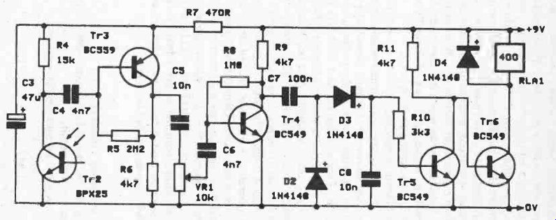
Fig. 37. The circuit diagram for the IR camera trigger
Circuit Operation
The necessary electronics for a system of this type can be very simple, and the basic set up is to have a transmitter which provides a beam of infrared pulses, plus a receiver circuit which detects any interruption of the signal and triggers the camera or flashgun.
What is required from the transmitter is therefore exactly the same as in the active infrared detector system described previously in this Section, and exactly the same circuit is used in this system. As this circuit (Figure 27) has already been described it will not be considered further here.
The receiver unit of the active infrared sensor could also be used in the present application, but it is less than ideal. Firstly, the relay would be energized under stand-by conditions and would be turned off when the beam was broken. This is not in itself a problem, as by using a set of normally closed relay contacts the required triggering of the camera or flashgun would be obtained when the beam was broken. However, it would mean that the relay would consume quite a lot of power, and as units of this type are usually battery powered in order to make them portable, this would result in a rather short battery life. It is therefore much better to use a modified circuit which switches on the relay when the beam is broken, and to use a set of normally open relay contacts to control the camera or flashgun.
Another worthwhile refinement is to add a sensitivity control.
Ideally the sensitivity of the receiver should be just high enough to reliably prevent the camera or flashgun from being spuriously triggered, so that anything even partially obscuring the beam activates the unit. This enables the unit to detect quite small insects (or whatever) which are not large enough to fully block the beam, or which in practice are unlikely to cut through the beam accurately enough to fully block it. The modified infrared receiver circuit appears in Figure 37, and this is clearly very similar indeed to the original circuit. The first difference is the inclusion of VR1 which operates as a volume control style variable gain control. In the smoothing circuit C8 has had its value reduced by a factor of ten in order to speed up the response time of the circuit to one which is more appropriate for the current application. At the output of the unit an inverter stage (Tr5 and R11) has been added between the smoothing circuit and the relay driver so that Tr6 and the relay are normally held in the off state, but are switched on when the beam is broken and Tr5 turns off.
Components for Camera Trigger (Fig. 37)
(Transmitter is as for the active infrared sensor unit, the list below is for the receiver circuit).
Resistors (all % watt 5% unless noted otherwise)
R4 15k R5 2M2 R6 4k7 R7 470R R8 1M8 R9 4k7
R10 3k3 R11 4k7
Potentiometer
VR1 10k log.
Capacitors
C3 47/110V elect C4 4n7 polyester C5 10n polyester C6 4n7 polyester C7 100n polyester C8 10n polyester
Semiconductors
Tr2 BPX25 Tr3 BC559 Tr4 BC549 Tr5 BC549 Tr6 BC549 D2 1N4148 D3 1N4148 D4 1N4148
Miscellaneous
RLA1 Coil resistance of about 200R or more suitable for nominal 9 volt operation, at least one set of normally open contacts of adequate rating for device to be controlled.
Case, circuit board, control knob, wire, solder, etc.
Construction
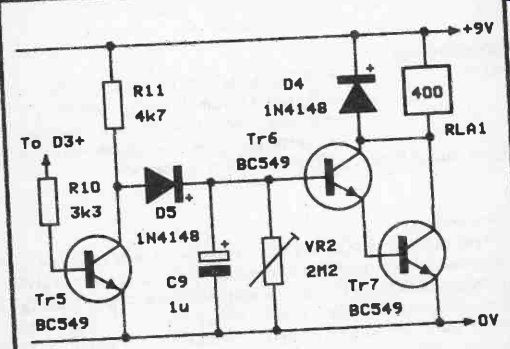
Fig. 38. The modified output stage with a hold -on facility
As pointed out before, the circuit has quite high gain and the component layout needs to be carefully designed in order to avoid problems with instability due to stray feedback. Apart from this construction of the system is quite straightforward, but unlike the active infrared sensor project, in this case the transmitter and receiver are built as entirely separate projects with each one having its own power source. This can be a 9 volt battery, but as the transmitter has a fairly high current consumption of something over 50 milliamps it is advisable to use a fairly high capacity battery for this unit.
A PP9 size battery or six HP7 size cells in a plastic holder should suffice.
The transmitter and receiver are both quite directional, and they must therefore be quite accurately aimed at one another in order to obtain sufficient pick up at the receiver to hold the relay in the "off' state.
A maximum range of over 1 meter should be obtained, and the range might be as much as 2 meters. This should be more than adequate for a camera trigger application.
Remember that for optimum sensitivity VR1 should be backed off to the point where the relay is only just kept in the "off' state.
For connection to a flashgun a flash extension lead will be needed, with the plug at the non -flashgun end being cut off so that the cable can be connected to the relay contacts. For connection to a camera or winder the appropriate electric release cable must be obtained, with the push button switch being removed to permit connection to the relay contacts. As the unit uses a relay to control the flashgun or camera, it provides a good simulation of a manually operated switch, and should work well with any camera, flashgun or winder.
The only exception to this is with some cameras and winders that are rather slow to operate, and which might not be operated reliably by the very brief pulse from the unit when a small object passes rapidly through the beam.
The solution to the problem is to use the modified output stage of Figure 38 which uses a simple charge storage circuit that holds the relay on for about one second once the unit has been activated. VR2 would normally be set at maximum resistance, but in the unlikely event of there being any problems with multiple triggering of the camera VR2 can be backed -off somewhat to give a shorter trigger period.
Fig. 39. A thyristor output stage for use with a flashgun.
If the unit is used with a flashgun the alternative output stage of Figure 39 might be preferred. This uses a thyristor or SCR (silicon controlled rectifier) to fire the flashgun, and the advantage of this method is that it is fully electronic and is consequently very fast.
Note that the thyristor must be a C106D or a similar type that will operate from a low gate current if it is to operate properly in this circuit. Also, the flash lead must be connected to the unit with the polarity indicated in Figure 39, and the correct polarity can be determined by checking the voltage across the flash-lead using a multimeter set to a high DC voltage range. No damage will result to the thyristor if the polarity of the flash lead is wrong, and trial and error can be used if a suitable multimeter is not available.
Infrared Communicator
The idea of using infrared for communications purposes is by no means a new idea, and systems for military use have been in existence for more than twenty years. In principle the idea is similar to the light beam telephone systems that are described in the electronics press from time to time, but with an infrared system the light beam is invisible, and there is no obvious sign of a communications link. Unlike radio communications systems, an infrared type is virtually tap -proof, and it is presumably these two security factors that made infrared communications systems attractive for military applications.
Whether or not infrared communications systems have any real advantage over other methods in non-military applications is debatable, but they certainly represent an interesting type of project for the electronics experimenter. Systems of this type could use a simple amplitude modulated beam system, like conventional light beam telephone designs, but infrared devices provide the wider bandwidth needed for a frequency modulation system, and this offers better quality results.
We will not consider the electronics of this system in any great detail as it is very similar to the fiber optic audio link which is described in Section 1. However, in this case the transmitter must operate with the low level output signal from a microphone, and an audio bandwidth of only about 3kHz is sufficient as we are only dealing with voice signals in this case.
Transmitter
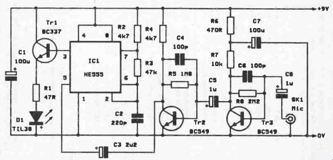
Fig. 40. The circuit diagram for the infrared communicator (transmitter section).
Figure 40 shows the circuit diagram for the transmitter. This has a 555 timer device acting as the voltage controlled oscillator, and the modulation input at pin 5 is driven from the output of a two stage common emitter amplifier. The latter provides a high level of voltage gain, but this is necessary as the unit is designed for operation with a low impedance dynamic microphone (the type sold as replacements for use with inexpensive cassette recorders), and these generally give an output of under 1 millivolt RMS. C4 and C6 provide high frequency roll off which helps to prevent high frequency signals from entering the VCO, and it also gives an improved signal to noise ratio. The carrier frequency is about 40kHz, which is more than adequate for a system which has considerably less than the full audio bandwidth.
Components for IR Communicator - Transmitter (Fig. 40)
Resistors (all 1/4 watt 5% unless noted otherwise)
R1 47R (1W)
R2 4k7 R3 47k R4 4k7 R5 1M8 R6 470R R7 10k R8 2M2
Capacitors
C1 100/4 10V elec
C2 220p ceramic plate
C3 2µ263V elect
C4 100p ceramic plate
C5 1/.4 63V elect
C6 100p ceramic plate
C7 100µ 10V elect
C8 1i.z 63V elect
Semiconductors
IC1 NE555
Tr1 BC337
Tr2 BC549
Tr3 BC549
D1 TIL38
Miscellaneous
SK1 3.5mm jack socket
Circuit board, case, lens (see text), wire, solder, etc.
Fig, 41. The main circuit diagram for the receiver section of the infrared
communicator
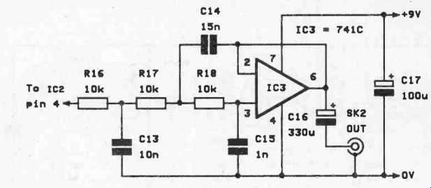
Fig. 42. The circuit diagram for the output filter
Receiver
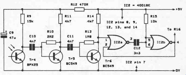
The main receiver circuit appears in Figure 41, but the output filter circuit appears separately in Figure 42.
The receiver has Tr4 as the infrared sensor followed by two high gain common emitter amplifiers. The two 2 input NOR gates of IC2 are wired to operate as a monostable multivibrator which acts as the demodulator. The other two gates of IC2 are left unused, but their inputs are connected to the positive supply rail to prevent spurious operation of them.
With some types of headphone and earphone it is possible to obtain quite good results if they are driven direct from the output of the monostable. However, results are generally better with an improved signal to noise ratio if some lowpass filtering is used at the output of the unit, and IC3 acts as the buffer amplifier in a third order lowpass filter having a cutoff frequency of approximately 3kHz. Although this filter provides an attenuation rate of only 18dB per octave, with the carrier frequency nearly four octaves above the cutoff frequency this still gives a high degree of carrier suppression (nearly 70dB in fact).
The receiver can drive most types of earphone and headphone, but it is not suitable for operation with low impedance earphones (crystal types are perfectly suitable though). With low and medium impedance headphones it is advisable to use series rather than parallel connection of the phones, and results will probably be much better with a resistor of about 47R connected in series with C16 if the unit is used with 8 or 16 ohm impedance types. The circuit could be used to drive a simple single IC audio power amplifier if loudspeaker operation is required, but bear in mind that if the unit is built as a two way system with loudspeaker output that transmit/receive switching will be needed. Simultaneous communications both ways is not feasible with loudspeaker output as it would result in acoustic "howl- around" Components for IR Communicator - Receiver (Figs. 41 and 42)
Resistors (all 1/4 watt 5%)
R9 15k R10 2M2 R11 4k7
R12 470R R13 1M8 R14 4k7 R15 to R18 10k (4 off)
Capacitors
C9 47µ 10V elect C10 4n7 polyester
C11 4n7 polyester C12 3n3 polyester
C13 10n polyester C14 15n polyester
C15 in polyester
C16 33011.10V elect
C17 100p. 10V elect
Semiconductors
IC2 4001BE IC3 741C Tr4 BPX25 or similar Tr5 BC549 Tr6 BC549
Miscellaneous
SK2 3.5mm jack socket
Case, circuit board, lens (see text), wire, solder, etc.
Construction and Use
This is another circuit which has a high level of voltage gain, and which consequently requires a carefully designed component layout. In this instance both the transmitter and the receiver contain high gain amplifiers, but the amplifier in the transmitter unit has a much more limited bandwidth which makes it very much less critical as far as the component layout is concerned.
Without the aid of an optical system the range of the unit is, to say the least, likely to be quite limited. In fact the maximum range is likely to be no more than two or three meters. However, with a simple system of lenses added this can easily be boosted by a factor of more than ten, giving a usable range of 30 meters or more. It is only fair to point out that a system of this type will not provide very. long ranges, as it is obviously a means of communications that is very much in the "line of sight" category.
With highly efficient lens systems it is supposedly possible to obtain ranges in excess of a kilometer, but a range as large as this is a little impractical in that aiming the transmitter and receiver units correctly becomes virtually impossible. Maintaining them in correct alignment would also be extremely difficult as the slightest knock to either unit could well be sufficient to cut communications.
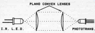
Fig. 43. The simple optical system for the infrared communicator
The optical system does not need to be anything very complex, and probably the best system to adopt is the one shown in Figure 43. This is similar to the optical system for the passive infrared beam project described previously, with a convex lens added in front of the receiving photocell so as to give it a larger pick up area and a very narrow angle of view. A lens of the same type is added in front of the transmitting photocell, and this has the effect of concentrating the infrared signal into a narrow beam. Figure 43 is slightly idealized in that it tends to suggest that there is no spreading of the beam from the transmitter, and that the receiver has a field of view which is equal to the diameter of the lens. This would give a range that was only limited by the attenuation of the infrared signal as it passed through the air, which would normally be many miles. On the other hand it would make alignment of the system practically impossible, and the fact that the beam spreads out as the range from the transmitter increases, and the viewing area of the receiver similarly increases, makes the system usable.
It does limit the range though, and if the range is boosted by using a more efficient optical system, setting up the equipment becomes more critical. The optical system therefore has to be chosen to give a good compromise between range and ease of setting up.
The lenses I used were a type having a diameter of 30 millimeters, and a focal length of 80 millimeters. The quality of the lenses is not important for an application of this type where we are only interested in roughly focusing a beam of light, and image quality is not a consideration. Inexpensive plastic types costing a few pence each are just as suitable as highly expensive color correct glass types costing many pounds. The lenses do not need to have the precise characteristics given previously, but they must be positive lenses (not concave types), and they should have a diameter of around 25 to 50 millimeters with a focal length of about 30 to 100 millimeters. The distance from the front of each photocell to its lens should be equal to the focal length of the lens, and in order to obtain good results the photocells should be accurately centered behind their lenses.
With even a very basic optical system the transmitter and receiver units need to be quite accurately aimed if good results are to be obtained. What seems to be the easiest way of doing things is to first aim the transmitter as accurately as you can by eye, and then use the receiver as a sort of field strength meter to determine exactly where the transmitter is actually aimed. With a little trial and error any necessary corrections to the aim can be made, so that the transmitter is known to be accurately aimed at the site where the receiver will be positioned. It is then just a matter of putting the receiver in place and adjusting its orientation for optimum results. The importance of getting the optical alignment correct can not be over -emphasized. With everything set up correctly it should be possible to obtain a good clear output signal with minimal background noise even at a range of 30 meters or so, but with the aim of one of the units even a couple of degrees out there may be no reception whatever. Remember that the units must be correctly aligned in two planes (horizontally and vertically) and not just laterally.
A two-way system is, of course, perfectly possible, but a transmitter and a receiver are needed at each end of the system, and there can be difficulties in aligning the system if they are built as a single unit. The problem is simply that as a receiver is turned to aim it correctly, the transmitter in the same box will be taken out of alignment. This can be overcome by first aiming the transmitter in the normal way, and then aligning the receiver by altering the position of the phototransistor behind the lens. This is much more difficult and awkward than it sounds, and it is actually much easier to construct each station of the system as separate transmitter and receiver units, or perhaps to have them as separate units but fitted on a single base which enables them to be individually aimed. In other words, to mount each unit on the base using some form of pan and tilt head, such as a type intended for photographic use.
Conclusion
Like the other projects described in this book, the infrared communicator represents an interesting and potentially useful project which is well worth trying. Modern opto-electronic devices offer good performance at low cost, and possibly represent the most interesting field of electronics for the experimenter.
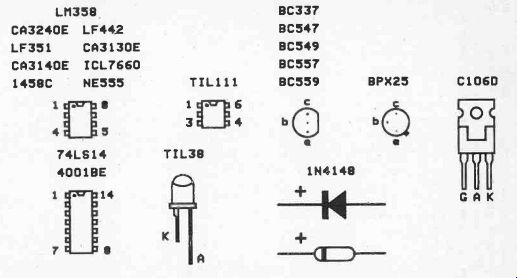
Fig. 44. Semiconductor pinout details (IC top views, transistor base views)