By ALLEN H. WOLACH
Substitute RAM for ROM
MOST one-board computers, particularly those intended for microprocessor training, contain an operating system and/or a limited high-level language in ROM and some small amount of user RAM. This RAM is usually sufficient to use the system for training purposes; but, after one becomes proficient, the need often arises for more user-memory space. Some systems provide for outboard memory but many do not. Although designed for the Heathkit ET-3400/ETA-3400 Computer Trainer/Trainer Accessory, the memory-expander approach described here can be adapted to other systems.
In this particular system, the Trainer Accessory contains Tiny BASIC in a 2K ROM. If this ROM is replaced with RAM, an additional 2048 bytes of user memory becomes available. If desired, the Tiny BASIC can be recorded on cassette and re-entered at any time using conventional cassette techniques.
Since the ROM is already placed in the system memory map, the address locations for the new RAM are safe. In actuality, the RAM connects to the system via the old ROM socket, thus no extensive wiring is required.
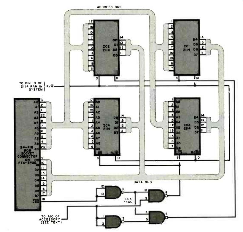
The 2114 static RAMs used in this project are 1K-x-4-bit types that have 1024 addresses with each addressing a 4-bit word. Thus, four 2114 RAMs create a 2048-x-8-bit memory.
In the ETA-3400, Tiny BASIC ROM pins 1 through 8, 22, and 23 are analogous to pins 1 through 7, 15, 16, and 17 of a 2114 RAM. On the ROM, pins 9, 10, 11, and 13 through 17 are the eight data I/O pins, while pins 11 through 14 are the four data I/O pins on the 2114.
Pins 21 (cs3) and 20 (cst) on the ROM are chip-select that are placed high (pin 21) and ground (pin 20) in the Heath System. These pins can be ignored since the 2114 RAM uses pin 8 (chip select) that is analogous to pin 18 (cs2) on the ROM. When the ROM is addressed, a circuit within the ETA-3400 decodes address lines A10 through Al5 and places a low at ai (pin 18) when the appropriate high addresses, A10 through A15, occur for any memory locations within the ROM. Since the Cs2 pin goes low for all 2K locations contained in the ROM, this line must be further decoded so that it goes low separately for the first and last half of the 2K locations. When the decoded input for the first half of the 2K locations goes low, the first half of the replacement 2K RAM is addressed; and, when the decoded input for the second half of the 2K locations goes low, the second half of the replacement RAM is similarly addressed.
The modification can be wired on a "solderless socket" having room for four 18-pin 2114s and one 14-pin 7400 TTL chip. Mount the ICs on the board with one unused row of connections between the ICs. Sockets are optional.
The 24-pin ROM socket connector is formed from a 24-pin DIP header. If such a header is difficult to locate, two 16-pin DIP headers can be suitably cut and cemented together in such a way as to form one 24-pin device.
The upper row of connectors on the solderless socket is connected to pin 24 on the 24-pin header to supply +5 volts to the RAM system. The bottom row of connectors on the solderless socket is connected to pin 12 on the 24-pin header to supply-5 volts (ground). The 2114 RAMs, IC1 through IC4, have their pins 9 connected to the ground line and their pins 18 connected to the +5-volt line. Pin 7 of IC5 is connected to ground and pin 14 to +5 volts.
The five ICs are wired in accordance with Fig. 1 and connected to the 24-pin header as shown. Use lead lengths long enough to reach the ROM socket in the ETA-3400. The address and data busses shown in Fig. 1 are for the RAM addition and are not the system busses. For example, pins 17 of IC2 and IC4 are connected to AO (address line 0) as do pins 1 of IC1 and IC3.
The cs2 modification is implemented by IC5 as shown in Fig. 1. In the Heath system, the line goes low for memory locations 1C00h through 23FFh. Address line 10 in the accessory is high for the first half of these locations (1 COOh through 1 FFFh) and low for the remaining locations between 2000h and 23FFh.
Thus, in the IC5 stage of Fig. 1, the output from pin 8 is negative for locations 1 COOh through 1 FFFh while the output from pin 6 is negative for locations 2000h through 23FFh.
Only two connections must be made to the computer accessory. First, pins 1, 2, and 9 of IC5 are connected (soldered) to A10 on the 40-pin connector of the accessory (pin 18 on the Heath 40-pin connector). Second, the R/w pin for the 2114 is pin 10. Interconnect pin 10 of each 2114 then connect them together via a length of wire to pin 10 of any one of the eight 2114 RAMs in the memory accessory.
Source: Computers and Electronics--Experimenter's Handbook (1984)
Also see: Using the 4060 as a Timer